TCAD Simulation and Analysis of Selective Buried Oxide MOSFET Dynamic Power


1
Department of Engineering and Science, Higher Colleges of Technology, PO Box 25026, Abu Dhabi, UAE
2
Department of Electrical Engineering, American University of Sharjah, PO Box 26666, Sharjah, UAE
*
Author to whom correspondence should be addressed.
J. Low Power Electron. Appl. 2019, 9(4), 29; https://0-doi-org.brum.beds.ac.uk/10.3390/jlpea9040029
Submission received: 6 August 2019
/
Revised: 15 September 2019
/
Accepted: 18 September 2019
/
Published: 22 September 2019
Abstract
:Low power consumption has become one of the major requirements for most microelectronic devices and systems. Increasing power dissipation may lead to decreasing system efficiency and lifetime. The BULK metal oxide semiconductor field-effect transistor (MOSFET) has relatively high power dissipation and low frequency response due to its internal capacitances. Although the silicon-on-insulator (SOI) MOSFET was introduced to resolve these limitations, other challenges were introduced including the kink effect in the current-voltage characteristics. The selective buried oxide (SELBOX) MOSFET was then suggested to resolve the problem of the kink effect. The authors have previously investigated and reported the characteristics of the SELBOX structure in terms of kink effect, frequency, thermal and static power characteristics. In this paper, we continue our investigation by presenting the dynamic power characteristics of the SELBOX structure and compare that with the BULK and SOI structures. The simulated fabrication of the three devices was conducted using Silvaco TCAD tools in 90 nm complementary metal oxide semiconductor (CMOS) technology. Simulation results show that the average dynamic power dissipation of the CMOS BULK, SOI and SELBOX are compatible at high frequencies with approximately 54.5 µW. At low frequencies, the SOI and SELBOX showed comparable dynamic power dissipation but with lower values than the BULK structure. The difference in power dissipation between the SELBOX and BULK is in the order of nano watts. This power difference becomes significant at the chip level. For instance, at 1 MHz, SOI and SELBOX exhibit an average dynamic power consumption of 0.0026 µW less than that of the BULK structure. This value cannot be ignored when a chip operates using thousands or millions of SOI or SELBOX MOSFETs.
1. Introduction
Power dissipation has assumed greater importance following the advent of portable battery driven devices such as laptops and cell-phones. Increasing a device’s power dissipation invariably results in increasing its temperature and reduces the battery life. The rise in temperature alters the device characteristics, and hence the reliability of the semiconductor device [1].
Dynamic power dissipation has become a significant concern because of the revolution in transistor scaling. As technology scales down, the channel length decreases, resulting in lower thresholds and supply voltages even though this achieves reliable circuits with less packaging costs. However, downscaling the channel length opens the door to other power dissipation problems, which also affect circuit efficiency [2]. The decreased die size and the increased number of transistors lead to a rapid increase in the power dissipation. The channel length and oxide thickness downscaling result in increasing the leakage current, and hence the leakage power, which is one form of static power dissipation.
Sources of power dissipation in metal oxide semiconductor (MOS) devices are both static and dynamic. Static power sources include the sub-threshold conduction when the transistor is in the OFF state [3], the tunneling current through gate oxide, which increases as the gate oxide thickness decreases, and the reverse bias current. The static current is dominated by threshold leakage when the complementary MOS (CMOS) is in weak inversion. Dynamic power dissipation has two main sources, the charging and discharging of the load capacitance () and the short circuit effect when both N-Channel MOSFET (NMOS) and P-Channel MOSFET (PMOS) transistors are in saturation.
Several approaches have been proposed in the literature to reduce static and dynamic power dissipation. Some of these approaches aim to reduce power dissipation through targeting the device architecture, which is the main scope of this work, and others have focused on circuit design. To reduce static power dissipation, Anis et al. [4] suggested using multi-threshold CMOS devices. A low threshold voltage for gate transistors that are in a critical path, and high threshold voltage for gate transistors in a non-critical path. This is due to the fact that sub-threshold conduction, which is one of the main causes of static power dissipation, decreases as the threshold voltage increases. However, this technique suffers from latency and complex fabrication.
Several methods have been used to reduce dynamic power dissipation in both BULK and SOI transistors including reducing the supply voltage , load capacitance , and the frequency [5]. Another published methodology for reducing dynamic power dissipation at the circuit-level is by clustering a number of gates and making one single large sleep transistor responsible for them [3]. However, when the structure is unbalanced with complicated interconnections, this methodology is not preferable and sharing one sleep transistor will increase the resistance of the interconnections [4]. Moreover, the size of the sleep transistor will get larger to compensate for the increased interconnect resistance. Innocenti et al. [5] suggested decreasing the dynamic power dissipation caused by short circuit effect, using reduced transistor width. This technique reduced the dynamic power dissipation by 20% when the transistor width was reduced by 45%. Furthermore, dynamic power dissipation was reduced by 20% by reducing the voltage supply. However, this technique increases the static power dissipation because decreasing the supply voltage is associated with decreasing the threshold voltage in order to maintain the desired circuit performance.
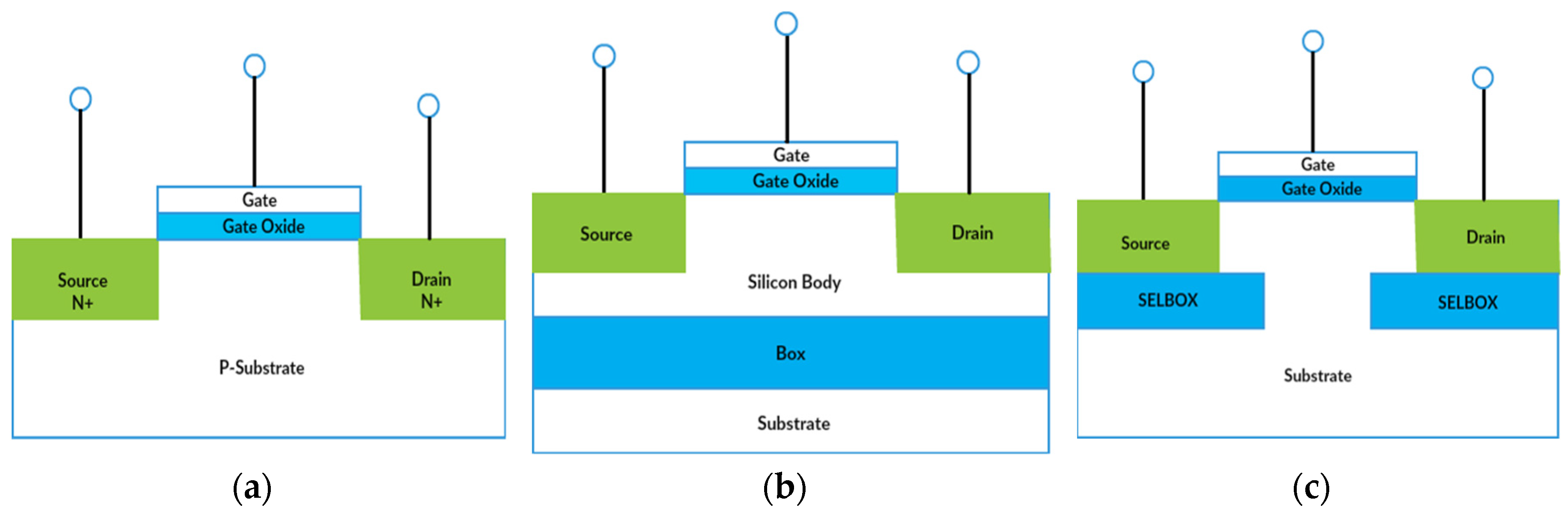
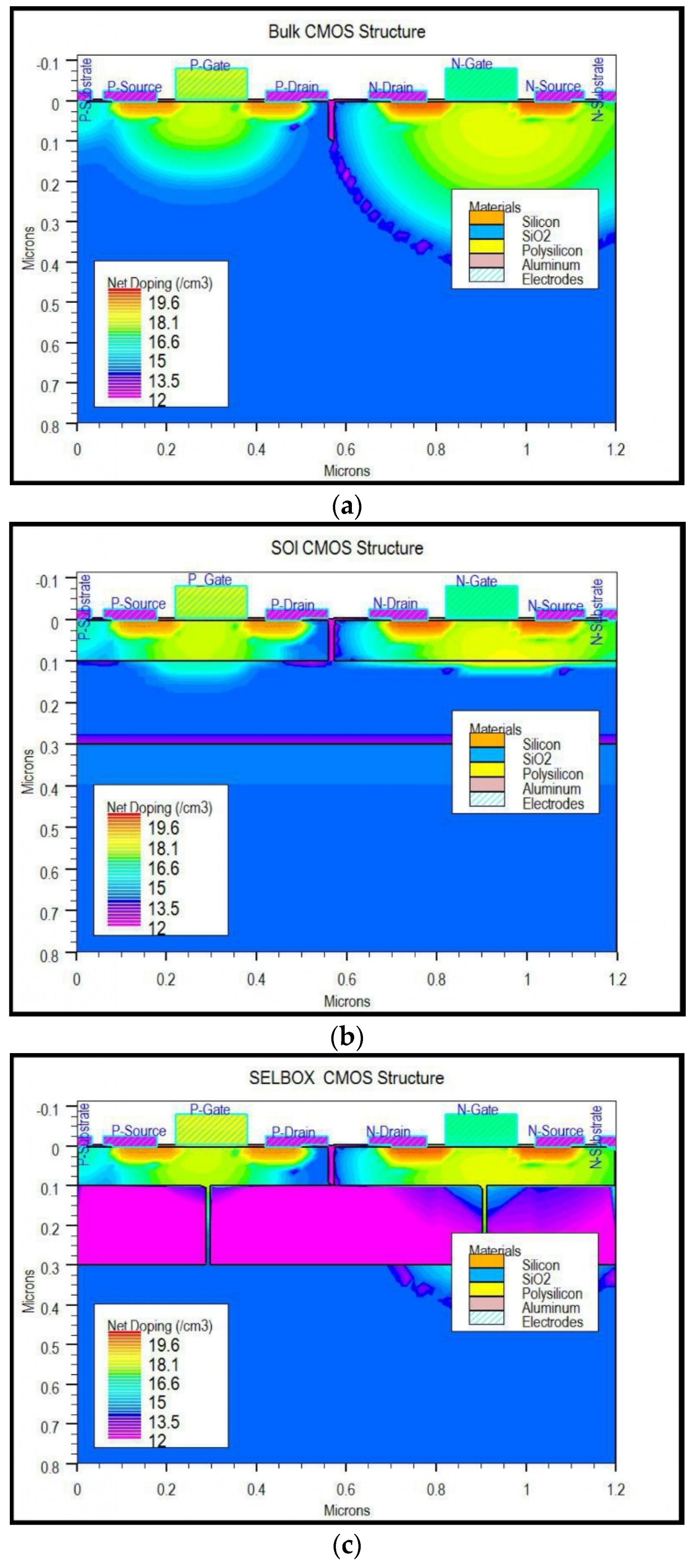
The conventional BULK transistor cross section shown in Figure 1a has some limitations associated with relatively high power dissipation, short channel effects and low speed due to the device’s internal capacitances. The SOI MOSFET shown in Figure 1b addresses several of the inherent limitations associated with BULK MOSFET devices. In SOI MOSFET devices, a layer of dielectric such as silicon dioxide is present in the silicon region below the source, drain and channel of the MOSFET. The newly introduced buried layer of oxide and vertical trench oxide electrically isolate the conduction region of the device from the lower substrate. The presence of buried oxide leads to a reduction in the parasitic capacitance leading to an overall improvement in the device performance [6]. Employment of the oxide layer minimizes the leakage currents and offers latch-up free operation in SOI CMOS devices [7].
In spite of the superior features of SOI MOSFET devices, the presence of the buried oxide layer leads to several undesirable effects such as the “self-heating effect” and “kink effect” [8,9]. The kink effect results from the accumulation of holes generated due to impact ionization at the drain end of the channel region. The device self-heating effect arises due to the poor thermal conductivity of the dielectric oxide layer and the associated temperature rise in the active device region. The kink effect leads to nonlinearity in the device current voltage characteristics. Self-heating leads to device failure if adequate measures are not taken to limit the temperature to safe levels.
The selective back oxide MOSFET (SELBOX MOSFET) was introduced as a remedial measure to minimize the issues associated with SOI MOSFET devices. In SOI MOSFET devices, the buried oxide (BOX) is present all the way from the regions below the source to the drain [10]. However, in SELBOX MOSFET, the buried oxide is present at selected regions below the source, drain and partially below the channel, as shown in Figure 1c. This structural modification enables heat transfer from the upper conduction region to the lower substrate and minimizes the problems due to self-heating in SOI MOSFET devices. Furthermore, in the modified structure with its low resistive gap between SELBOX segments, the SELBOX structure is effective in minimizing the rise in the body potential and the non-linearity in the output current voltage characteristics. The authors have conducted a detailed investigation on the SELBOX MOSFET and observed the abilities of the modified structure to reduce self-heating and kink effects [8,9,11].
The presence of buried oxide has improved effects on the leakage currents in the CMOS units employing SOI and SELBOX MOSFETs as compared to the CMOS made of conventional BULK MOSFET devices. The reduction in the leakage currents results from the high resistive dielectric segments introduced in the structure by the oxide regions. Consequently, the on-state and off-state leakage currents and static power dissipation was found to be superior to BULK CMOS devices, as verified by authors in their previous work [12].
One of the fundamental aspects that decides the frequency characteristics of a semiconductor device is the parasitic capacitance. The presence of buried oxide in SOI devices and in SELBOX devices reduces the parasitic capacitances. As a result, the frequency response of the circuits employing SOI and SELBOX was found to be superior to the BULK MOSFTs [8]. Another important implication of reduced parasitic capacitance is the reduction in the charging and discharging currents when the CMOS unit turns on and off. With reduced charging and discharging currents, the power associated with the turn-on and off events will also be low. Hence, we hypothesize that using the SELBOX structure may reduce the dynamic power dissipation. Therefore, the main objective of this work is to investigate the dynamic power dissipation of the SELBOX structure and compare it with the BULK and SOI structures. The simulation of device fabrication was conducted using Silvaco TCAD tools [13].
The rest of the paper is organized as follows: Section 2 presents the methodology used for determining the dynamic power dissipation by calculations and simulation. Section 3 describes the simulated fabrication of CMOS BULK, SOI and SELBOX devices. Section 4 discusses the results followed by the conclusions and discussion in Section 5.
2. Methodology
In this section we describe the mechanism behind dynamic power dissipation in CMOS inverter circuits. We also explain how to estimate this type of power dissipation using device parameters or from simulated voltage and current signals.
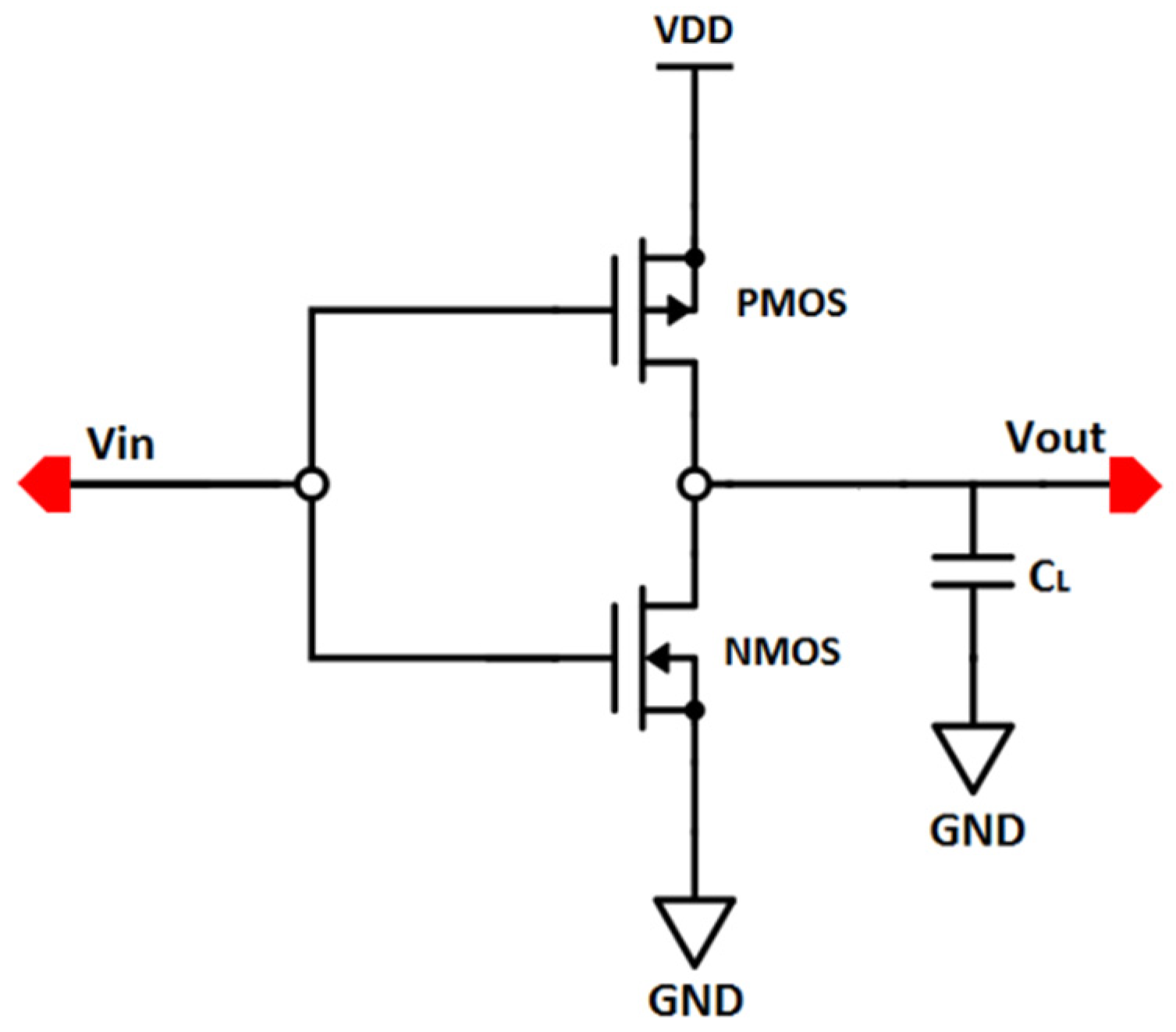
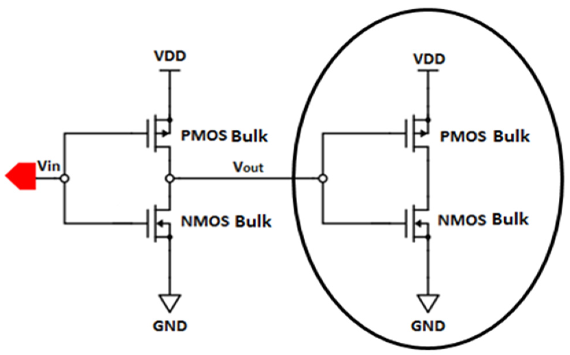
The CMOS inverter circuit is shown in Figure 2. It is composed of a pull-up network, PMOS; and a pull-down network, NMOS and a driving load .
When a pulse signal of 1.0 ps rise and fall time and 10 ns pulse width is applied to the input of the inverter, the output voltage takes time to fully charge or discharge , as depicted in the output voltage shown in Figure 3. During the output voltage transition from a low to high state, load capacitance is charged by current while dissipating power in PMOS resistance . However, during the transition from a high to low state, is discharged while power is dissipated in the NMOS resistance . The dynamic power dissipation in BULK technology is the dominant factor in power dissipation in CMOS devices down to 180 nm, but is questionable in SOI and SELBOX [3].
Theoretically, the dynamic power dissipation in the CMOS inverter may be computed using [14]:
where is the clock frequency, is the supply voltage and is the activity factor, which is the probability of the output switching from 0 to 1. As the signal used in this simulation work is a clock (pulse) signal, is equal to 1 [15]. includes the internal capacitances of the NMOS and PMOS in the CMOS inverter and the internal capacitances of the NMOS and PMOS of the load, assuming the CMOS inverter is driving another CMOS inverter as a load as depicted in Equation (2) [16]:
where and are the gates that drain the capacitance of the NMOS and PMOS of the CMOS inverter, respectively. and are the drains to Bulk capacitance of the NMOS and PMOS in the CMOS inverter, respectively. and are the gate capacitance of the NMOS and PMOS of the CMOS inverter load. is the wiring capacitance.
Another source of dynamic power dissipation is the short circuit power dissipation. During the transition from the ON to OFF state or from the OFF to ON state, there will be a period of time where both PMOS and NMOS transistors are conducting and the current will find a direct path between and ground, thus resulting in short circuit current. The short circuit power dissipation is [3]:
where voltage, is the fall or rise time of the input signal and is the clock frequency and is a factor that depends on the transistor dimensions [14].
If the device parameters and dimensions are available, we can estimate the average dynamic power dissipation in the CMOS inverter by adding the power dissipation in both PMOS and NMOS [16]. It can be shown that the total average dynamic power dissipation is:
where is the clock period. Furthermore, to determine the dynamic power dissipation in the simulated devices, we can use numerical integration of the used voltage and current signals:
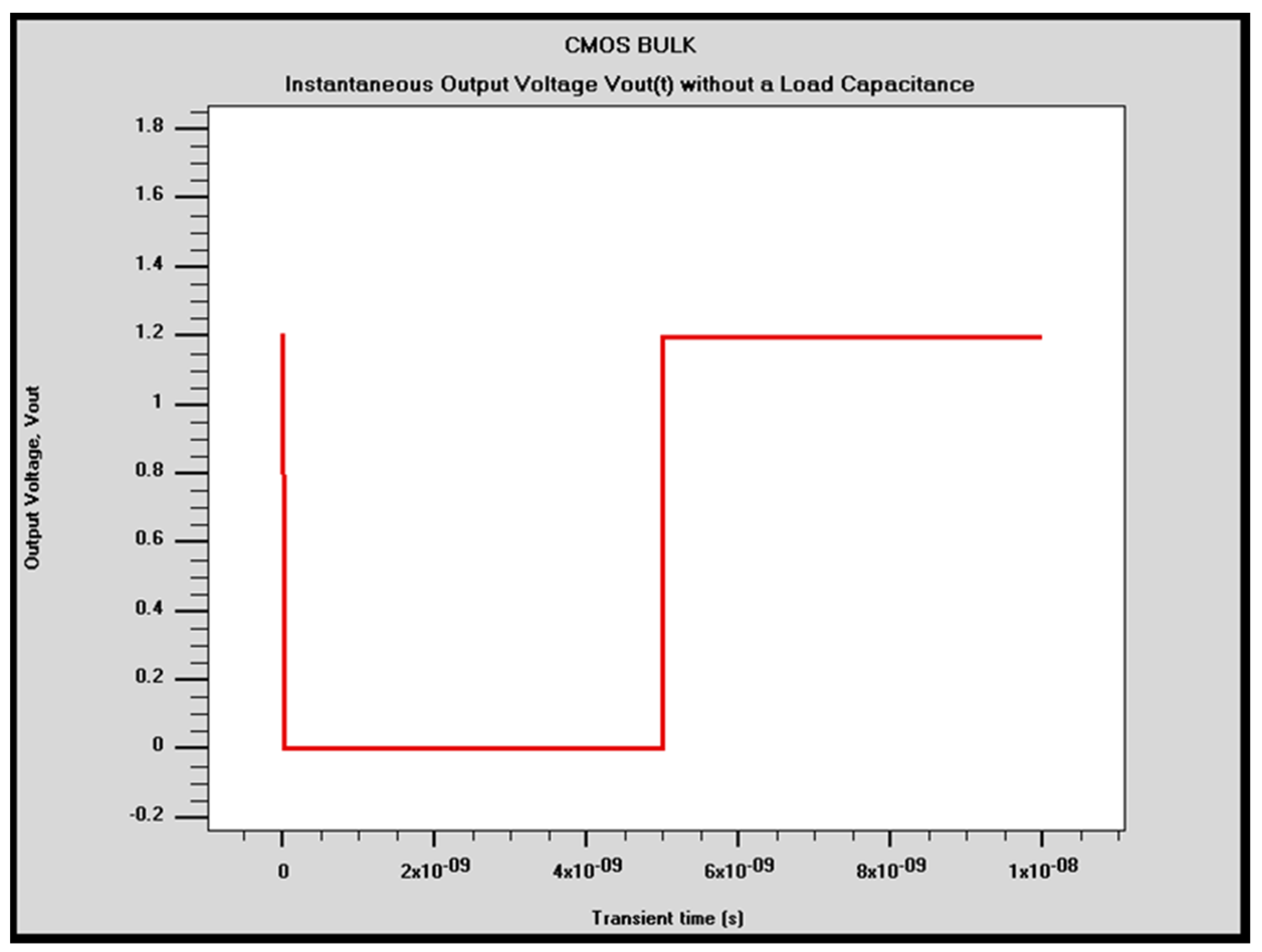
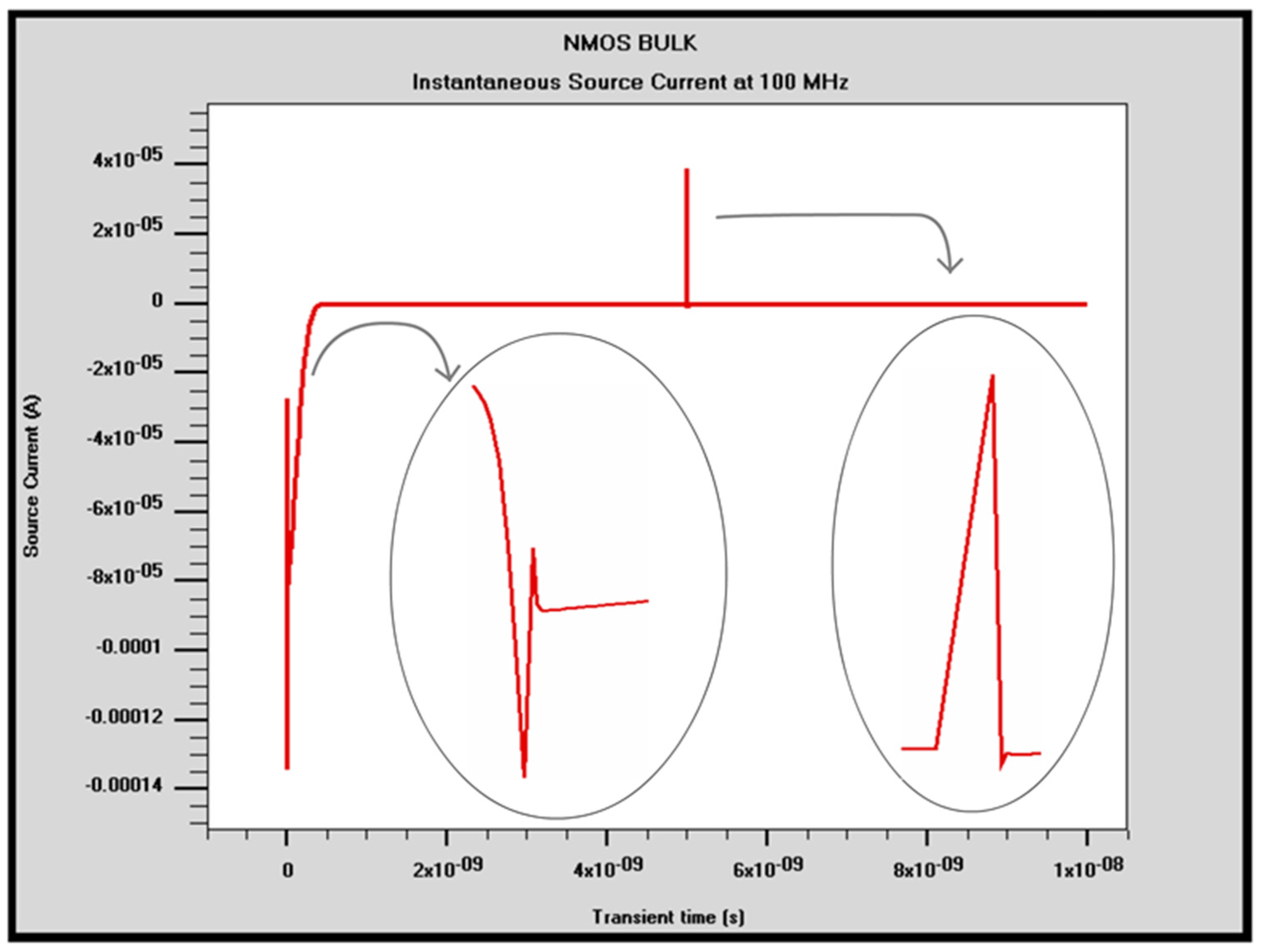
where and are the NMOS and PMOS source currents, respectively. Thus, if f = 100 MHz, total average dynamic power dissipation can be estimated by integrating the voltage and current signals depicted in Figure 3 and Figure 4 using Equation (5). This method will be used later on in the Results section.
3. Simulation of Device Fabrication
3.1. Design and Dimensions
The three CMOS devices are in length and wide. The channel length is 90 nm. The aspect ratio is the same for all simulated devices and architectures. However, in practice, the channel width of the PMOS is 2 times wider than the NMOS to compensate for the mobility difference. The channel length of 90 nm was chosen because static power dissipation becomes significant in 90 nm CMOS technology and beyond [17]. The dimensions and simulated fabrication of the CMOS devices for BULK structure are shown in Table 1 and Figure 5a. Moreover, the CMOS SOI simulated fabrication was achieved by inserting an isolation layer in the substrate of the CMOS BULK as seen in Figure 5b according to the dimensions in Table 2. The SELBOX CMOS simulated fabrication was conducted with dielectric isolation of the active NMOS and PMOS regions from the substrate as depicted in Figure 5c. The dielectric employed in this case is not continuous between the source and drain as in SOI devices. The dielectric segments cover regions below the source and drain and partially cover the region below the channel according to the following dimensions listed in Table 3.
3.2. Device Parameters
Three major device parameters were calculated and simulated: the threshold voltage , the mobility , and the oxide capacitance . These parameters were calculated and simulated using estimated parameters found from simulation and fabrication of similar devices, as listed in Table 4. Using Table 4, and were estimated to be and , respectively. The N-channel and P-channel mobilities were estimated using Table 5 and found to be and , respectively. Consequently, the N-channel is better than the P-channel in switching applications. However, the P-channel devices have high noise immunity, are easy to control and have low cost processing. is the transport factor, , and are fitting parameters.
4. Results
In this section, we investigate the effect of varying the operating frequency on the dynamic power dissipation of the three CMOS architectures. First, was set to a typical load capacitance value of and the average dynamic power dissipation against frequency was obtained. Unfortunately, a discrete load capacitance may not be a realistic scenario. This is because the load capacitance is the sum of internal capacitances of the load device and it is assumed to be the same for the three structures. If a digital system is composed of CMOS devices of the same structure; such as a system where all devices are BULK, SOI or SELBOX, it is more realistic to assume that represents the internal capacitance of the CMOS load which has the same structure. This is an important test as it reveals the actual dynamic power dissipation which occurs in real electronic systems. Thus, in the second test, we investigated the dynamic power dissipation by considering a CMOS BULK driving a CMOS BULK, a CMOS SOI driving a CMOS SOI, and a CMOS SELBOX driving a CMOS SELBOX load. In both simulation tests, the dynamic power dissipation was calculated using Equations (4) and (5) described in the Methodology section.
4.1. Effect of Varying the Operating Frequency with Discrete
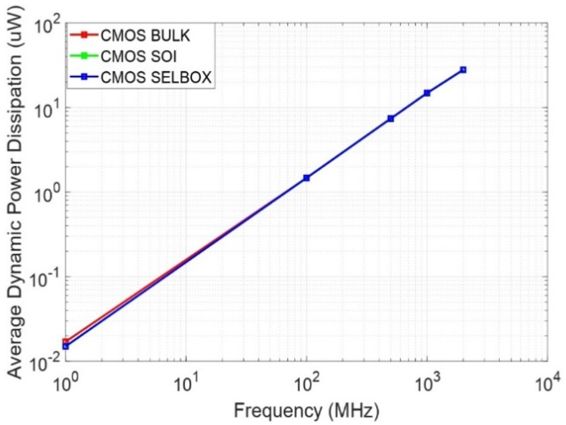
In this test, only the operating frequency was varied whilst keeping and fixed. The simulation was carried out by applying a pulse signal of rise and fall times with the pulse width varying according to the selected frequency. The test was carried out for practical frequencies ranging from to . is discrete and was assumed to be . The supply voltage was set to which is the standard supply voltage used for technology [18]. The CMOS inverter circuit used to carry out this test is shown in Figure 2. The average dynamic power dissipation was calculated using Equation (5). Table 6, Table 7 and Table 8 show the average dynamic power dissipation for the three structures. The results indicate that as switching frequency increases, power dissipation increases as expected according to the model described in Equation (1). The average dynamic power dissipation of the three devices show very small differences at high and low frequencies. For instance, at 1 MHz, the average dynamic power dissipation of the BULK CMOS is higher than that of the SOI and SELBOX by 0.002 µW. However, at 2 GHz, the average dynamic power dissipation of the BULK is similar to that of SELBOX SOI and higher than SOI by 0.1 µW.
Figure 6 summarizes the CMOS BULK, SOI and SELBOX average dynamic power dissipation against frequency. It can be observed that the curves are linear, indicating identical behavior with very small differences. It can also be observed that as frequency increases, average dynamic power dissipation increases as expected. This is because is discrete and assumed to be the same for the three devices. In addition, the channel resistance of the NMOS in all three devices is almost the same. The same applies to the channel resistance of the PMOS. However, their structural difference resides in the internal capacitance. All three devices have different internal capacitance, and hence is not the same when it is considered as a lumped device. For instance, in the work of Narayanan et al., different values of were found, that is, , and for CMOS BULK, SOI and SELBOX, respectively [8]. This case will be discussed further in the next subsection.
4.2. Effect of Varying the Operating Frequency with CMOS Load
A reasonable assumption is that all devices in a system have the same technology and structure. Thus, a CMOS BULK drives a CMOS BULK, a CMOS SOI drives a CMOS SOI and a CMOS SELBOX drives a CMOS SELBOX as a load. Based on this assumption, the CMOS BULK inverter circuit is presented as shown in Figure 7, where the circled device is the load. The same circuit configuration applies to SOI and SELBOX inverter circuits. The same procedure described in the Methodology section was used to estimate the average dynamic power dissipation. However, in this simulation a similar CMOS device was used as the load instead of a capacitor.
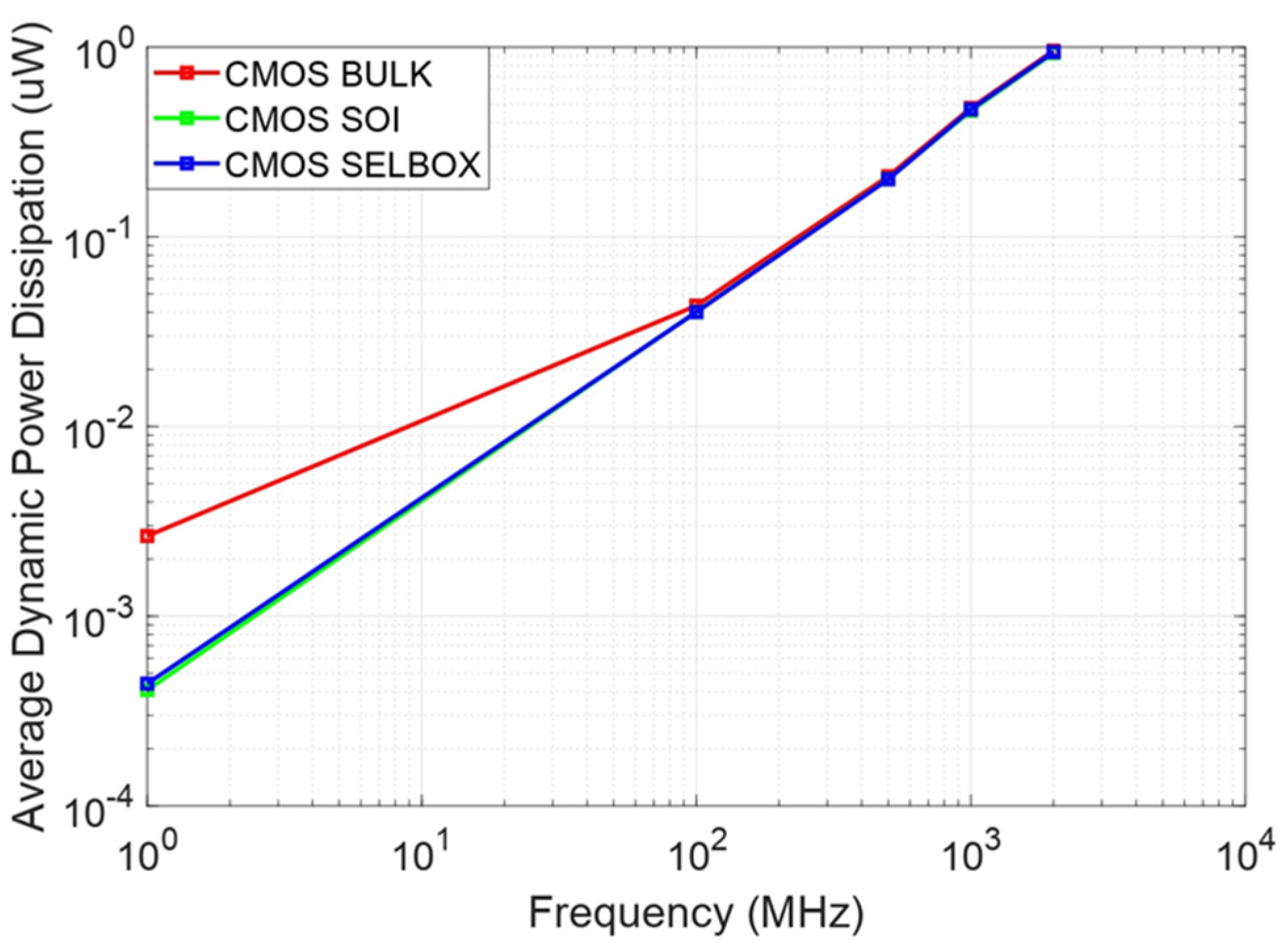
Table 9 lists the average dynamic power dissipation results for CMOS BULK, SOI and SELBOX. As frequency increases, the average dynamic power dissipation increases as expected. Figure 8 shows the combined average dynamic power dissipation for the three structures. The results show that the CMOS BULK has the highest average dynamic power dissipation. CMOS SOI and SELBOX have very close average dynamic dissipation results. However, the CMOS SOI average dynamic power dissipation is slightly lower than that of CMOS SELBOX while the latter’s average dynamic power dissipation lies in between that of the CMOS BULK and SOI. This is because the CMOS SOI reduces the device’s parasitic capacitances more than the CMOS SELBOX, as a result of inserting the BOX layer. Moreover, the results in Figure 8 show that the deviation in the average dynamic power dissipation of the three CMOS devices occurs at low frequencies. Yet, at high frequencies, the average dynamic power dissipation is almost the same for the CMOS BULK, SOI and SELBOX. This is because the parasitic capacitances behave like a resistor at high frequency, leading to higher average dynamic power dissipation. However, at low frequencies, the SOI and SELBOX structures exhibit lower parasitic capacitances than the BULK structure.
4.3. Dynamic Power Dissipation Using Device Parameters
This section presents the results obtained using the mathematical model of the average dynamic power dissipation of the CMOS BULK, SOI and SELBOX devices. Moreover, it provides a justification for the average dynamic power dissipation results when the operating frequency is varied.
The total power dissipation is the addition of the average dynamic power dissipation which is dissipated in the PMOS because of the charging and discharging of . Thus, the average dynamic power dissipation is calculated using Equation (4). The calculation of the average dynamic power dissipation when the operating frequency is is explained in the following paragraphs.
To calculate and , the time constants and are found from the CMOS inverter output in Figure 3, where is the time taken for the output to fall from 90% to 37% of its maximum value, which is 0.444 V. However, is the time taken for the output to rise from 10% to 63% of its maximum value, which is equal to 0.756 V. Discharging and charging time constants and are equal to and s, respectively. Hence, and are found to be Ω and , respectively. Then, after finding , , and , the total average dynamic dissipation is calculated using Equation (4) to be
The same procedure was followed to calculate the average dynamic power dissipation in CMOS SOI and SELBOX. Table 10 shows the calculated values of the average dynamic power dissipation in CMOS SOI and SELBOX at 100 MHz. It is worth mentioning that the same CL value that was used in calculating the average dynamic power dissipation in CMOS BULK, was also used to find that of CMOS SOI and SELBOX.
Comparing the results of the simulation and the calculations for CMOS BULK, SOI and SELBOX, it can be seen that the results are the same with approximately 2.1% error. As such, the similarities in the simulation and calculation results show that the procedure for finding the dynamic power dissipation for the three CMOS devices in the simulation was reasonably accurate.
5. Conclusion and Discussion
In this work, the average dynamic power dissipation of the SELBOX structure was investigated and compared to that of SOI and BULK structures. The SELBOX’s properties enable it to have a low self-heating effect, eliminate the kink effect, and operate at high speed. Its structure reduces the device’s internal capacitances, and hence reduces the dynamic power dissipation compared to the BULK CMOS structure [12,19].
The dynamic power dissipation was investigated for the three CMOS architectures by varying the operating frequency. All test results showed that as frequency increases, average dynamic power dissipation increases. Moreover, the average dynamic power dissipation results for the three devices showed a similar behavior when the load was a discrete capacitor. This is because the load capacitance was assumed to be the same for the three devices and their channel resistances were almost the same. However, assuming the CMOS is driving a load that has the same structure reveals the actual load capacitance, and hence, the average dynamic power dissipation results showed differences for the three devices. The CMOS SELBOX has the lowest average dynamic power dissipation and the CMOS BULK has the highest although it is very close to that of the CMOS SOI.
Furthermore, it was noticed that the average dynamic power dissipation of the three CMOS devices is not the same at low frequencies. However, at high frequencies, the average dynamic power dissipation of the three devices are almost the same. This is because, at high switching frequency, the parasitic capacitances behave like a resistor, and hence losses increase, which results in increasing average dynamic power dissipation. On the other hand, the second test showed that as the load capacitance increases, the average dynamic power dissipation increases as expected.
Fair and exact comparison with state-of-the-art devices is challenging because of the different technology, materials and specifications that are used. In addition, most of the recent publications report the total power dissipation produced by the whole system rather than a single CMOS device. Nevertheless, we mention here the results of a couple of recent publications on the dynamic power dissipation. Baker stated in his book that a CMOS inverter designed using 50 nm and operated at 4 GHz produced 19.6 µW [20]. At a system level, a CMOS inverter comparator based on 90 nm technology was reported in [21]. The average reported power consumption was 24.3 μW.
In conclusion, the CMOS SELBOX structure is better than the CMOS SOI structure in eliminating kink and self-heating effects and shows almost the same average dynamic power dissipation as that of CMOS SOI. Also, the CMOS SELBOX structure is better than the CMOS BULK structure in providing reduced internal capacitances, and thus lower average dynamic power dissipation and better frequency characteristics.
The average dynamic power dissipation calculations were very close to those found from the simulation, with approximately 2.1% percentage of error.
Author Contributions
Investigation, R.M.; Methodology, R.M.; Project administration, H.A.-N.; Resources, N.M.; Software, N.M.; Supervision, H.A.-N.; Writing—original draft, R.M.; Writing—review & editing, H.A.-N.
Funding
This research was funded by the College of Engineering at the American University of Sharjah.
Acknowledgments
The authors would like to thank Dana Younis for introducing Rana to the use of TCAD tools in her research and for her constructive suggestions on the manuscript.
Conflicts of Interest
The authors declare no conflict of interest.
References
- Fanciulli, C.; Abedi, H.; Merotto, L.; Dondè, R.; De Iuliis, S.; Passaretti, F. Portable thermoelectric power generation based on catalytic combustor for low power electronic equipment. Appl. Energy 2018, 215, 300–308. [Google Scholar] [CrossRef]
- Piguet, C. Low-Power CMOS Circuits: Technology, Logic Design and CAD Tools; CRC: Boca Raton, FL, USA, 2004. [Google Scholar]
- Nam Sung, K.; Austin, T.; Baauw, D.; Mudge, T.; Flautner, K.; Hu, J.; Irwin, M.; Kandemir, M.; Narayanan, V. Leakage current: Moore’s law meets static power. Computer 2003, 36, 68–75. [Google Scholar] [CrossRef]
- Anis, M.; Areibi, S.; Mahmoud, M.; Elmasry, M. Dynamic and leakage power reduction in MTCMOS circuits using an automated efficient gate clustering technique. In Proceedings of the 2007 44th ACM/IEEE Design Automation Conference, New Orleans, LA, USA, 10–14 June 2002; pp. 480–485. [Google Scholar]
- Innocenti, J.; Welter, L.; Julien, F.; Lopez, L.; Sonzogni, J.; Niel, S.; Regnier, A.; Paire, E.; Labory, K.; Denis, E.; et al. Dynamic power reduction through process and design optimizations on CMOS 80 nm embedded non-volatile memories technology. In Proceedings of the 2014 IEEE 57th International Midwest Symposium on Circuits and Systems (MWSCAS), College Station, TX, USA, 3–6 August 2014; pp. 897–900. [Google Scholar]
- Kuo, J.B.; Lin, S.C. Low Voltage SOI CMOS VLSI Devices and Circuits; Wiley: New York, NY, USA, 2001. [Google Scholar]
- Chandrakasan, A.; Brodersen, R. Low-Power CMOS Design; Wiley: New York, NY, USA, 1998; pp. 105–110. [Google Scholar]
- Narayanan, M.R.; Al-Nashash, H.; Pal, D.; Chandra, M. Frequency response of MOS devices with SELBOX structure. In Proceedings of the 2012 16th IEEE Mediterranean Electrotechnical Conference, Yasmine Hammamet, Tunisia, 25–28 March 2012; pp. 1099–1102. [Google Scholar]
- Narayanan, M.; Al-Nashash, H.; Mazhari, B.; Pal, D.; Chandra, M. Analysis of kink reduction in SOI MOSFET using selective back oxide structure. Act. Passiv. Electron. Compon. 2012, 2012, 565827. [Google Scholar] [CrossRef]
- Pal, C.; Mazhari, B.; Iyer, S. Simulation of MOSFET Devices and Circuits Fabricated on Selective Buried Oxide (SEL-BOX) Substrates. In Proceedings of the IEEE Conference on Electron Devices and Solid-State Circuits (EDSSC 2005), Hong Kong, China, 19–21 December 2005. [Google Scholar]
- Narayanan, M.R.; Al-Nashash, H.; Pal, D.; Chandra, M. Thermal model of MOSFET with SELBOX structure. J. Comput. Electron. 2013, 12, 803–811. [Google Scholar] [CrossRef]
- Younes, D.; Madathumpadical, N.R.; Al-Nashash, H. Static Power Characteristics of Selective Buried Oxide CMOS Devices. Int. J. Numer. Model. Electron. Netw. Devices Fields 2019, 32, e2460. [Google Scholar] [CrossRef]
- Silvaco. Atlas User’s Manual Device Simulation Software; Silvaco: Santa Clara, CA, USA, 2010. [Google Scholar]
- Zeghbroeck, B. Principles of Semiconductor Devices; Colorado University: Boulder, CO, USA, 2011. [Google Scholar]
- Weste, N.; Harris, D. CMOS VLSI Design: A Circuits and Systems Perspective, 4th ed.; Wesley: Reading, MA, USA, 2011. [Google Scholar]
- Constantinescu, F.; Maruna, N.; Marin, R.; Marin, M. Simulation of a Ring Oscillator with CMOS Inverters; University Politehnica Bucharest: Bucharest, Romania, 2011. [Google Scholar]
- Sedra, A.; Smith, K. Microelectronic Circuits: Theory and Applications; Oxford University Press: Oxford, UK, 2013. [Google Scholar]
- Yang, C.-Y.; Li, S.-Y.; Hsieh, S.C.-L.; Liu, J.Y.-C. A push-push voltage-controlled oscillator for W-band applications in 90-nm CMOS. In Proceedings of the 2016 IEEE International Symposium on Radio-Frequency Integration Technology (RFIT), Taipei, Taiwan, 24–26 August 2016; pp. 1–3. [Google Scholar]
- Younis, D.; Madathumpadical, N.; Al-Nashash, H. Modeling and simulation of static power dissipation in CMOS with SELBOX structure. In Proceedings of the 2017 7th International Conference on Modeling, Simulation, and Applied Optimization (ICMSAO), Sharjah, UAE, 4–6 April 2017; pp. 1–4. [Google Scholar]
- Baker, R. CMOS Circuit Design Layout and Simulation, 4th ed.; Wiley-IEEE Press: Indianapolis, IN, USA, 2019. [Google Scholar]
- Bhatia, V.; Pandey, N.; Bhattacharyya, A. High Speed Power Efficient CMOS Inverter Based Current Comparator in UMC 90 nm Technology. Int. J. Electr. Comput. Eng. 2016, 6, 90. [Google Scholar] [CrossRef]
Figure 1.
MOSFET structures: (a) BULK NMOS, (b) silicon-on-insulator (SOI), (c) selective buried oxide (SELBOX).
Figure 1.
MOSFET structures: (a) BULK NMOS, (b) silicon-on-insulator (SOI), (c) selective buried oxide (SELBOX).

Figure 2.
Dynamic switching power in CMOS inverter.

Figure 3.
Instantaneous output voltage Vout (t) at 100 MHz.

Figure 4.
Instantaneous NMOS source current at 100 MHz.

Figure 5.
Simulated fabrication of CMOS devices: (a) BULK CMOS, (b) SOI CMOS and (c) SLEBOX CMOS structures.
Figure 5.
Simulated fabrication of CMOS devices: (a) BULK CMOS, (b) SOI CMOS and (c) SLEBOX CMOS structures.

Figure 6.
Average dynamic power dissipation vs. frequency, = 10 fF.

Figure 7.
CMOS BULK inverter driving another CMOS BULK inverter circuit.

Figure 8.
Average dynamic power dissipation vs. frequency, load.


Table 1.
CMOS BULK structure dimensions.
| Dimensions | NMOS | PMOS |
|---|---|---|
| Channel length | 90 nm | 90 nm |
| Average Oxidization Thickness | 6.3 nm | 6.3 nm |
| Average Doping Length | 50 nm | 50 nm |
| Isolation Thickness in Between | 100 nm | 100 nm |
Table 2.
CMOS SOI structure dimensions.
| Dimensions | NMOS | PMOS |
|---|---|---|
| Channel length | 90 nm | 90 nm |
| Average Oxidization Thickness | 6.3 nm | 6.3 nm |
| Average Doping Length | 50 nm | 50 nm |
| Isolation Thickness in Between | 100 nm | 100 nm |
| Isolation Width | 0.2 µm | 0.2 µm |
Table 3.
CMOS SELBOX structure dimensions.
| Dimensions | NMOS | PMOS |
|---|---|---|
| Channel length | 90 nm | 90 nm |
| Average Oxidization Thickness | 6.3 nm | 6.3 nm |
| Average Doping Length | 50 nm | 50 nm |
| Isolation Thickness in Between | 100 nm | 100 nm |
| Isolation Width | 0.2 µm | 0.2 µm |
| Gap Length | 9 nm | 9 nm |
Table 4.
Device parameters.
| Device Parameter | Value | Unit |
|---|---|---|
| Doping concentration of poly silicon () | ||
| Doping concentration of substrate ( | ||
| Boltzmanns constant | ||
| Room Temperature | ||
| Charge density | Coulomb | |
| Permittivity of oxide | ||
| Permittivity of silicon | ||
| Electron affinity of the semiconductor | ||
| Bulk potential () | ||
| Oxide thickness |
Table 5.
The parameters used to calculate the mobility as a function of the doping density.
| Constants | Phosphorus | Boron | Units |
|---|---|---|---|
| 68.5 | 44.9 | ||
| 1414 | 470.5 | ||
| A | 0.711 | 0.719 | Null |
Table 6.
Dynamic power dissipation results for CMOS BULK.
| Frequency f (MHz) | Period T (ps) | |||
|---|---|---|---|---|
| 1 | 1,000,000 | 0.01 | 0.01 | 0.017 |
| 100 | 10,000 | 0.74 | 0.74 | 1.47 |
| 500 | 2000 | 3.68 | 3.70 | 7.38 |
| 1000 | 1000 | 7.36 | 7.39 | 14.8 |
| 2000 | 500 | 14.70 | 13.2 | 27.9 |
Table 7.
Dynamic power dissipation results for CMOS SOI.
| Frequency f (MHz) | Period T (ps) | |||
|---|---|---|---|---|
| 1 | 1,000,000 | 0.007 | 0.0073 | 0.015 |
| 100 | 10,000 | 0.74 | 0.73 | 1.47 |
| 500 | 2000 | 3.69 | 3.69 | 7.38 |
| 1000 | 1000 | 7.38 | 7.38 | 14.8 |
| 2000 | 500 | 14.70 | 13.1 | 27.8 |
Table 8.
Dynamic power dissipation results for CMOS SELBOX.
| Frequency f (MHz) | Period T (ps) | |||
|---|---|---|---|---|
| 1 | 1,000,000 | 0.007 | 0.007 | 0.015 |
| 100 | 10,000 | 0.74 | 0.73 | 1.47 |
| 500 | 2000 | 3.69 | 3.70 | 7.39 |
| 1000 | 1000 | 7.38 | 7.38 | 14.8 |
| 2000 | 500 | 14.70 | 13.2 | 27.9 |
Table 9.
Average dynamic power dissipation in CMOS BULK, SOI and SELBOX.
| Frequency f (MHz) | Period T (ps) | |||
|---|---|---|---|---|
| 1 | 1,000,000 | 0.003 | 0.0004 | 0.0004 |
| 100 | 10,000 | 0.043 | 0.04 | 0.04 |
| 500 | 2000 | 0.209 | 0.20 | 0.20 |
| 1000 | 1000 | 0.479 | 0.46 | 0.47 |
| 2000 | 500 | 0.958 | 0.93 | 0.94 |
Table 10.
Average dynamic power dissipation calculations for CMOS SOI and SELBOX at 100 MHz.
| Parameter | CMOS SOI | CMOS SELBOX |
|---|---|---|
| 112.5 | 112.4 | |
| 160 | 140 | |
| (KΩ) | 11.25 | 11.24 |
| (KΩ) | 16 | 14 |
| 1.44 | 1.44 |
© 2019 by the authors. Licensee MDPI, Basel, Switzerland. This article is an open access article distributed under the terms and conditions of the Creative Commons Attribution (CC BY) license (http://creativecommons.org/licenses/by/4.0/).
Share and Cite
MDPI and ACS Style
Mahmoud, R.; Madathumpadical, N.; Al-Nashash, H. TCAD Simulation and Analysis of Selective Buried Oxide MOSFET Dynamic Power. J. Low Power Electron. Appl. 2019, 9, 29. https://0-doi-org.brum.beds.ac.uk/10.3390/jlpea9040029
AMA Style
Mahmoud R, Madathumpadical N, Al-Nashash H. TCAD Simulation and Analysis of Selective Buried Oxide MOSFET Dynamic Power. Journal of Low Power Electronics and Applications. 2019; 9(4):29. https://0-doi-org.brum.beds.ac.uk/10.3390/jlpea9040029
Chicago/Turabian StyleMahmoud, Rana, Narayanan Madathumpadical, and Hasan Al-Nashash. 2019. "TCAD Simulation and Analysis of Selective Buried Oxide MOSFET Dynamic Power" Journal of Low Power Electronics and Applications 9, no. 4: 29. https://0-doi-org.brum.beds.ac.uk/10.3390/jlpea9040029
Note that from the first issue of 2016, this journal uses article numbers instead of page numbers. See further details here.