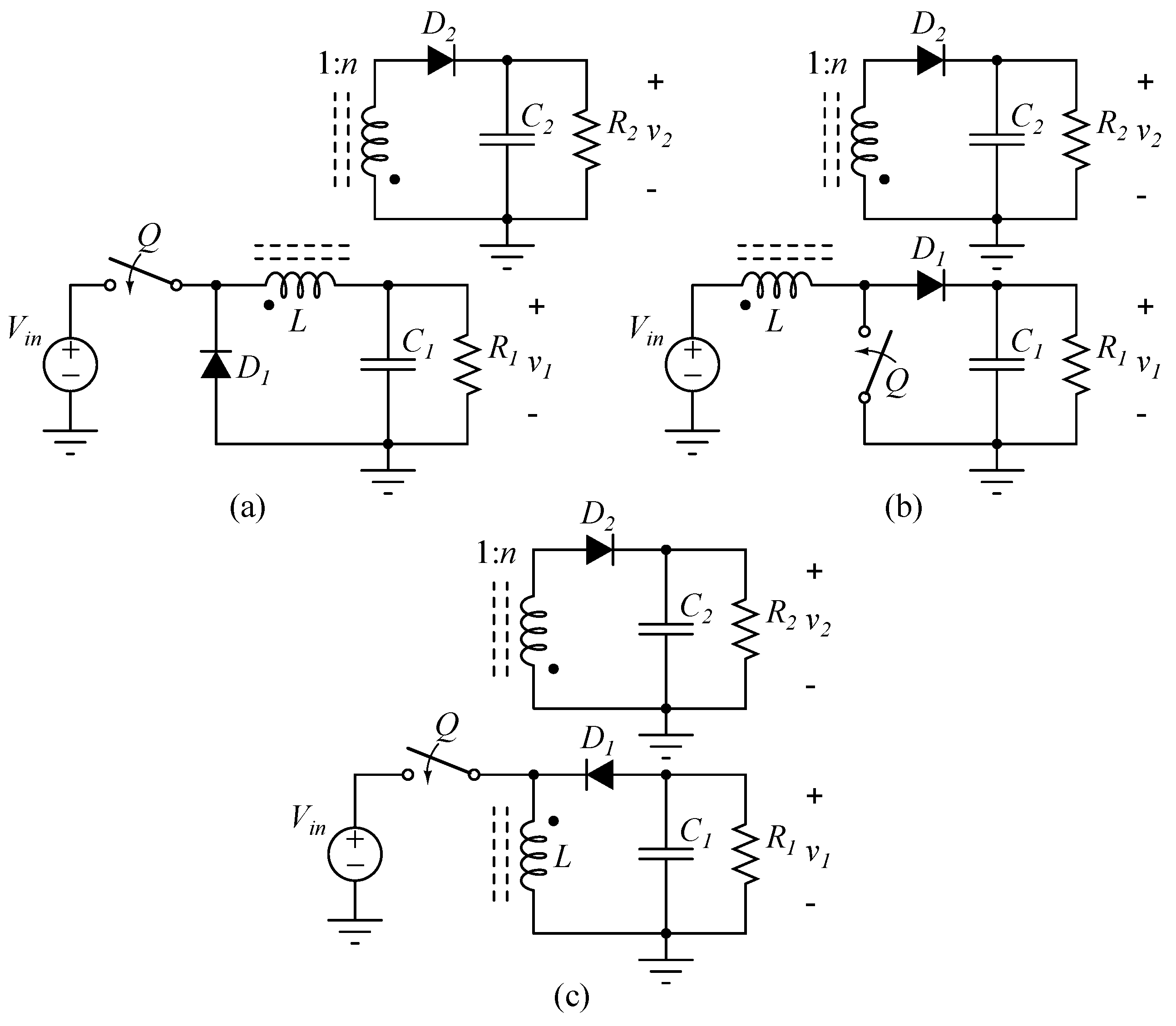
Figure 1.
(a) A two-output buck converter. (b) A potential two-output boost converter; (c) A potential two-output buck-boost converter.
Figure 1.
(a) A two-output buck converter. (b) A potential two-output boost converter; (c) A potential two-output buck-boost converter.
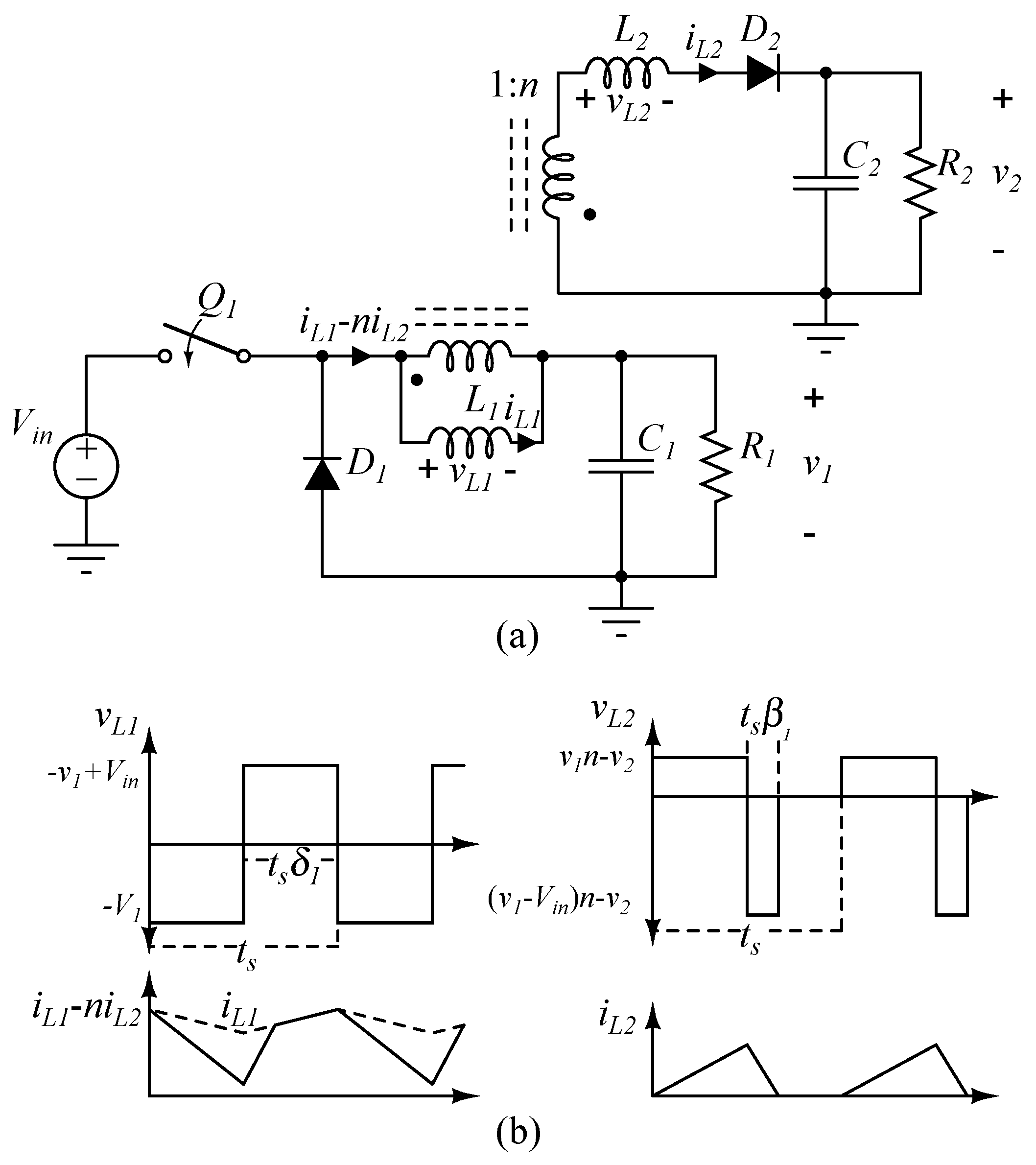
Figure 2.
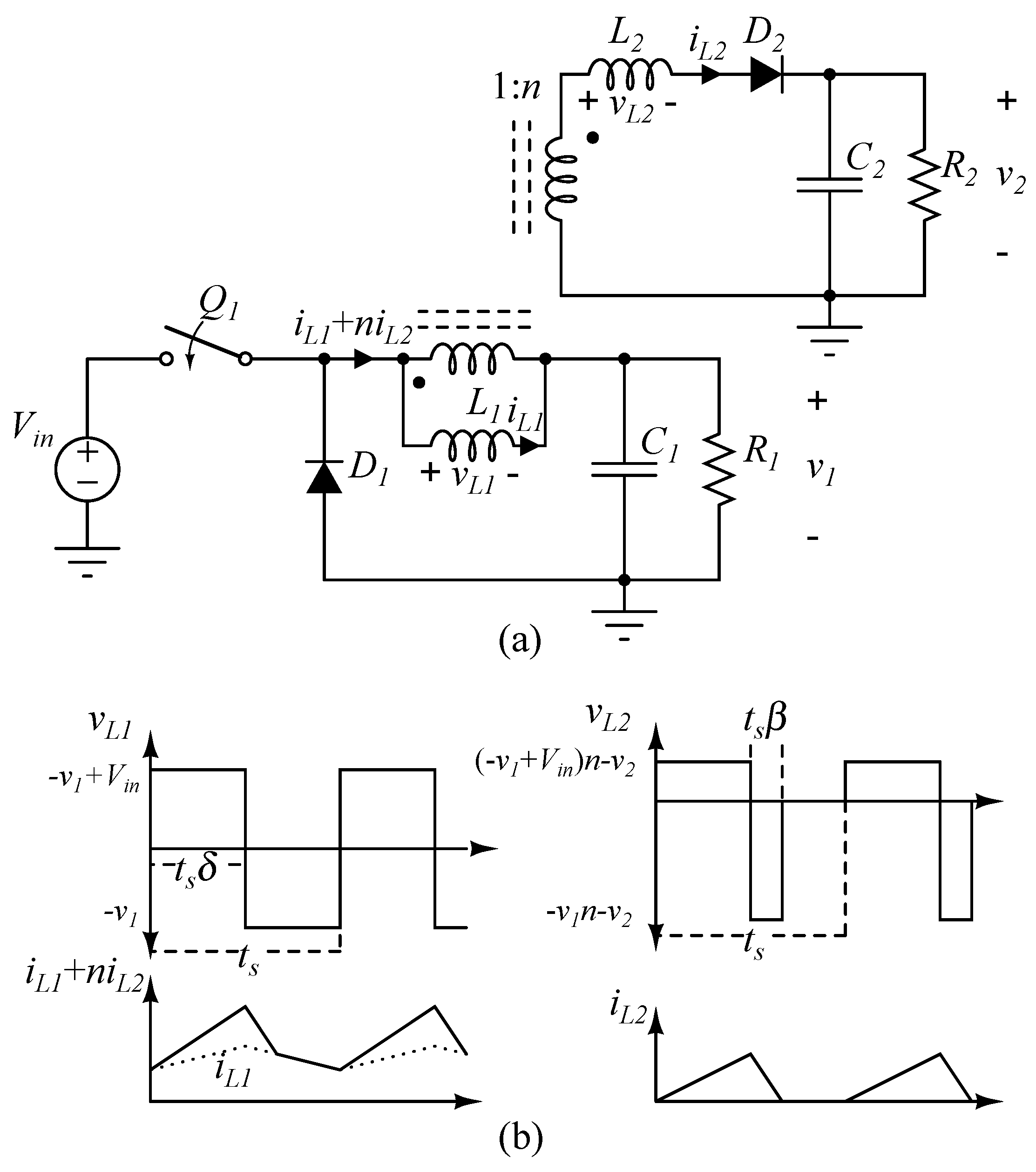
(a) A fly-buck type two-output buck converter; (b) Voltage and current waveforms of the magnetizing and leakage inductances of the coupled inductor v, i-ni, v and i, respectively.
Figure 2.
(a) A fly-buck type two-output buck converter; (b) Voltage and current waveforms of the magnetizing and leakage inductances of the coupled inductor v, i-ni, v and i, respectively.
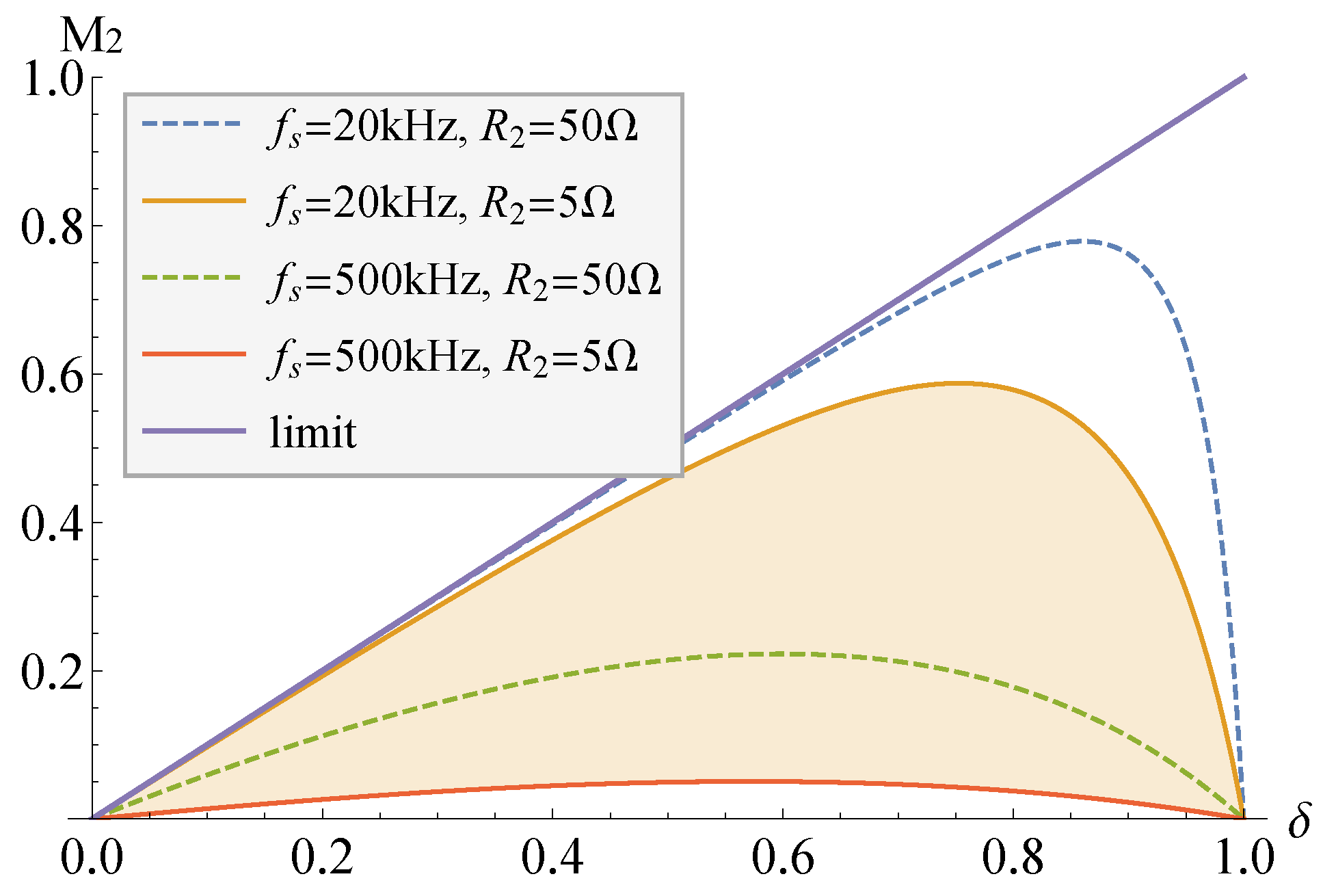
Figure 3.
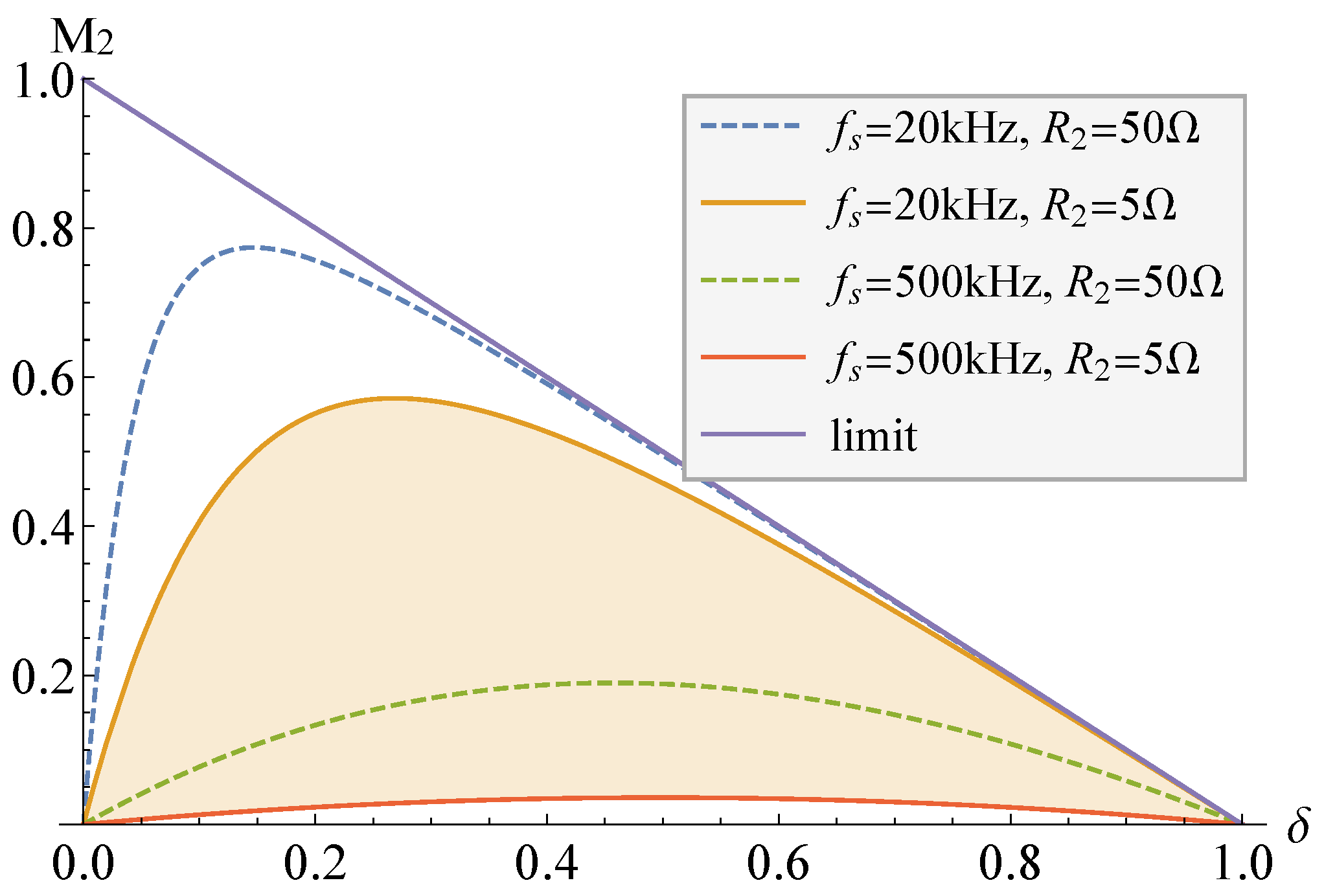
Conversion ratio of the second output, M
=
v/
V, versus the duty cycle
at different switching frequencies
f combined with the second load
R of the fly-buck converter when the turns ratio of the coupled inductor
n is 1. For the other components, see
Table 1. Results are obtained by using (
1).
Figure 3.
Conversion ratio of the second output, M
=
v/
V, versus the duty cycle
at different switching frequencies
f combined with the second load
R of the fly-buck converter when the turns ratio of the coupled inductor
n is 1. For the other components, see
Table 1. Results are obtained by using (
1).
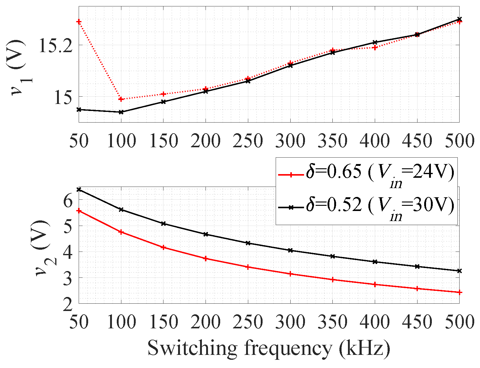
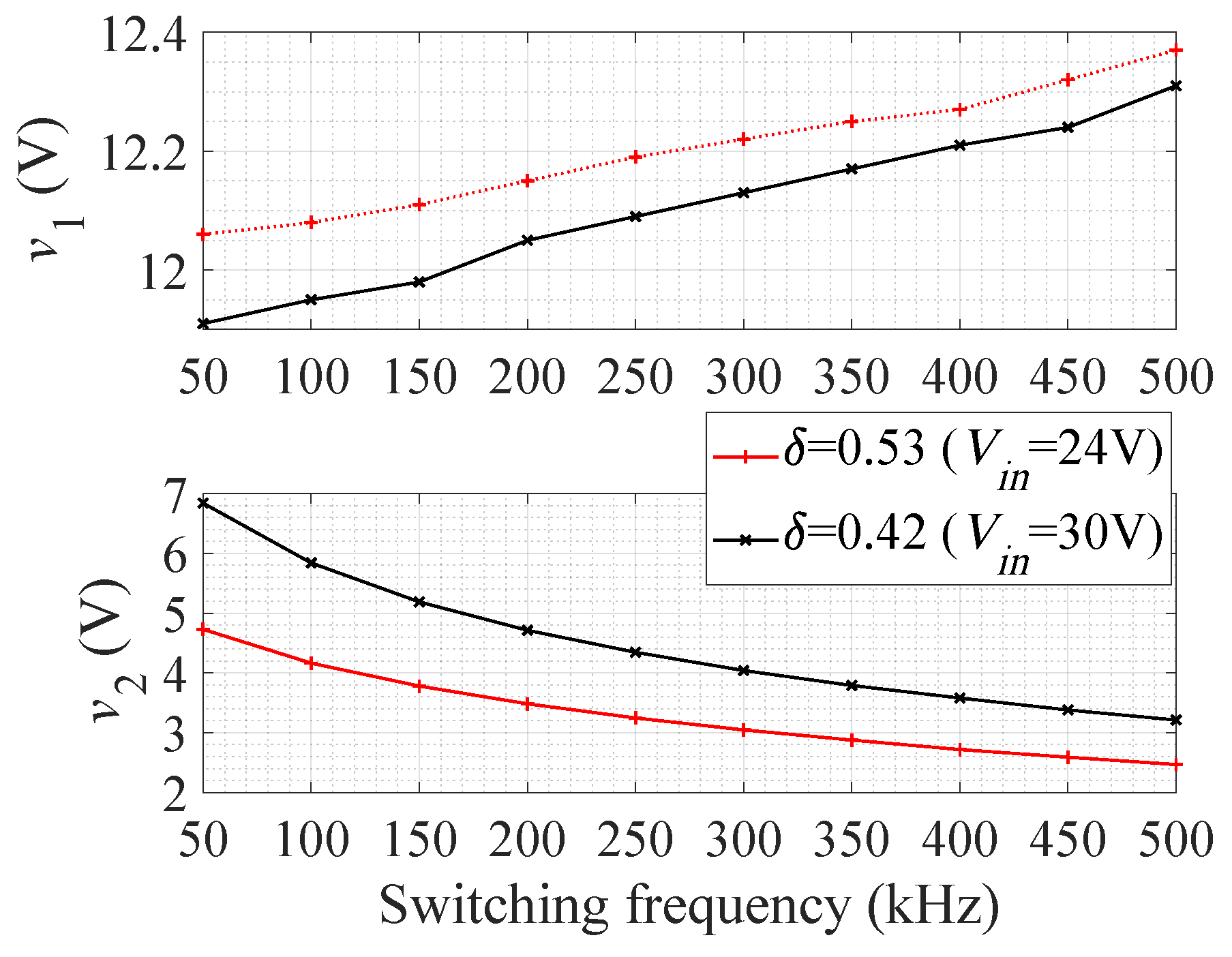
Figure 4.
Experimentally measured output voltages of the proposed fly-buck two-output converter for different f (R = 10 and R = 6.25 ).
Figure 4.
Experimentally measured output voltages of the proposed fly-buck two-output converter for different f (R = 10 and R = 6.25 ).
Figure 5.
(a) Forward-buck type two-output buck converter; (b) Voltage and current waveforms of the magnetizing and leakage inductances of the coupled inductor v, i + ni, v and i, respectively.
Figure 5.
(a) Forward-buck type two-output buck converter; (b) Voltage and current waveforms of the magnetizing and leakage inductances of the coupled inductor v, i + ni, v and i, respectively.
Figure 6.
The conversion ratio of the second output of the forward-buck two-output converter, M
=
v/
V, versus the duty cycle
at different
f, and the second load
R. The turns ratio of the coupled inductor
n is 1. For the other components, see
Table 1. Results are obtained by using (
5).
Figure 6.
The conversion ratio of the second output of the forward-buck two-output converter, M
=
v/
V, versus the duty cycle
at different
f, and the second load
R. The turns ratio of the coupled inductor
n is 1. For the other components, see
Table 1. Results are obtained by using (
5).
Figure 7.
Experimentally measured output voltages of the proposed forward-buck two-output converter depending on f (R = 12 and R = 8.3 ).
Figure 7.
Experimentally measured output voltages of the proposed forward-buck two-output converter depending on f (R = 12 and R = 8.3 ).
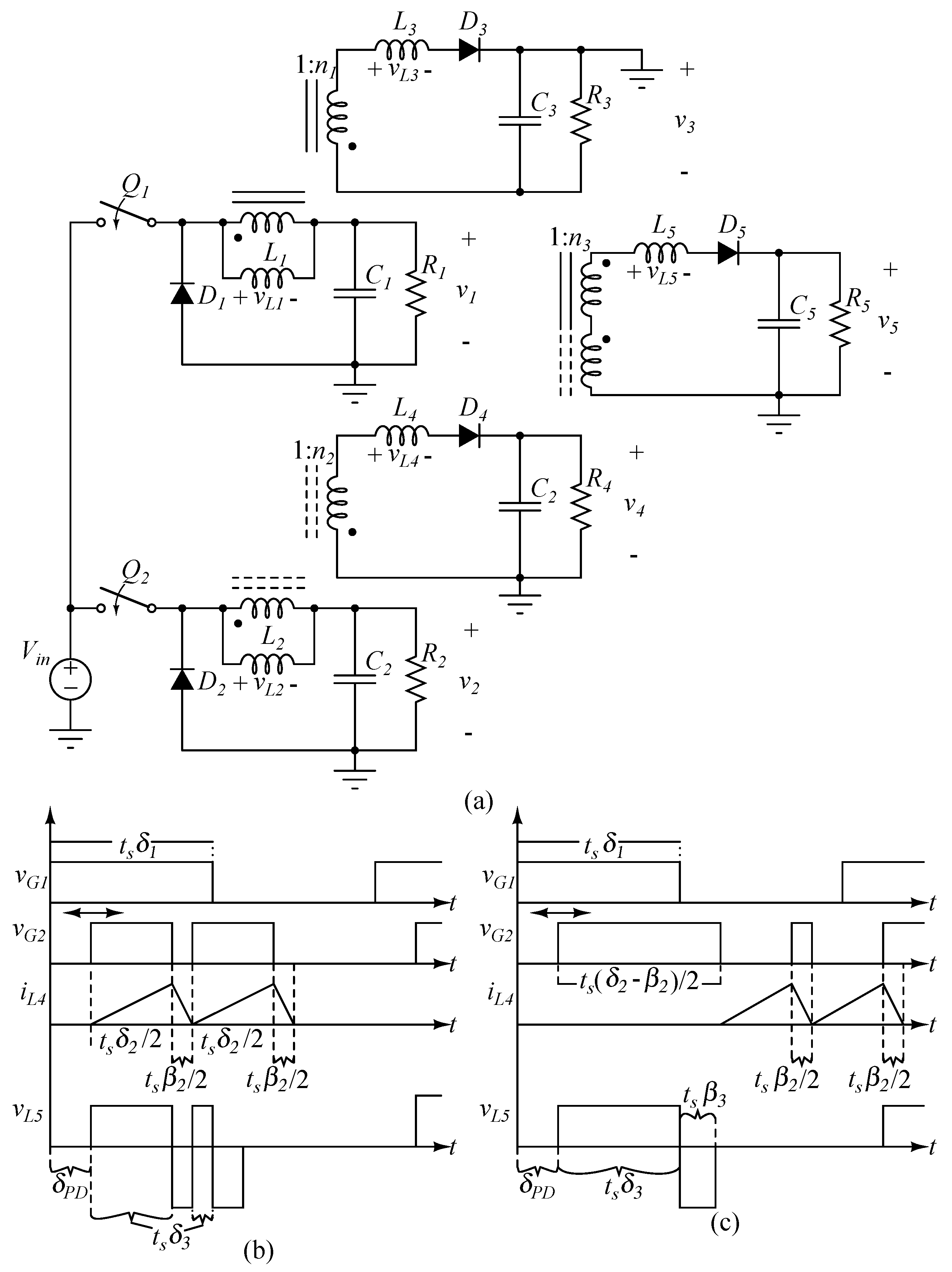
Figure 8.
PWM-PD controlled three-output forward-type buck converter.
Figure 8.
PWM-PD controlled three-output forward-type buck converter.
Figure 9.
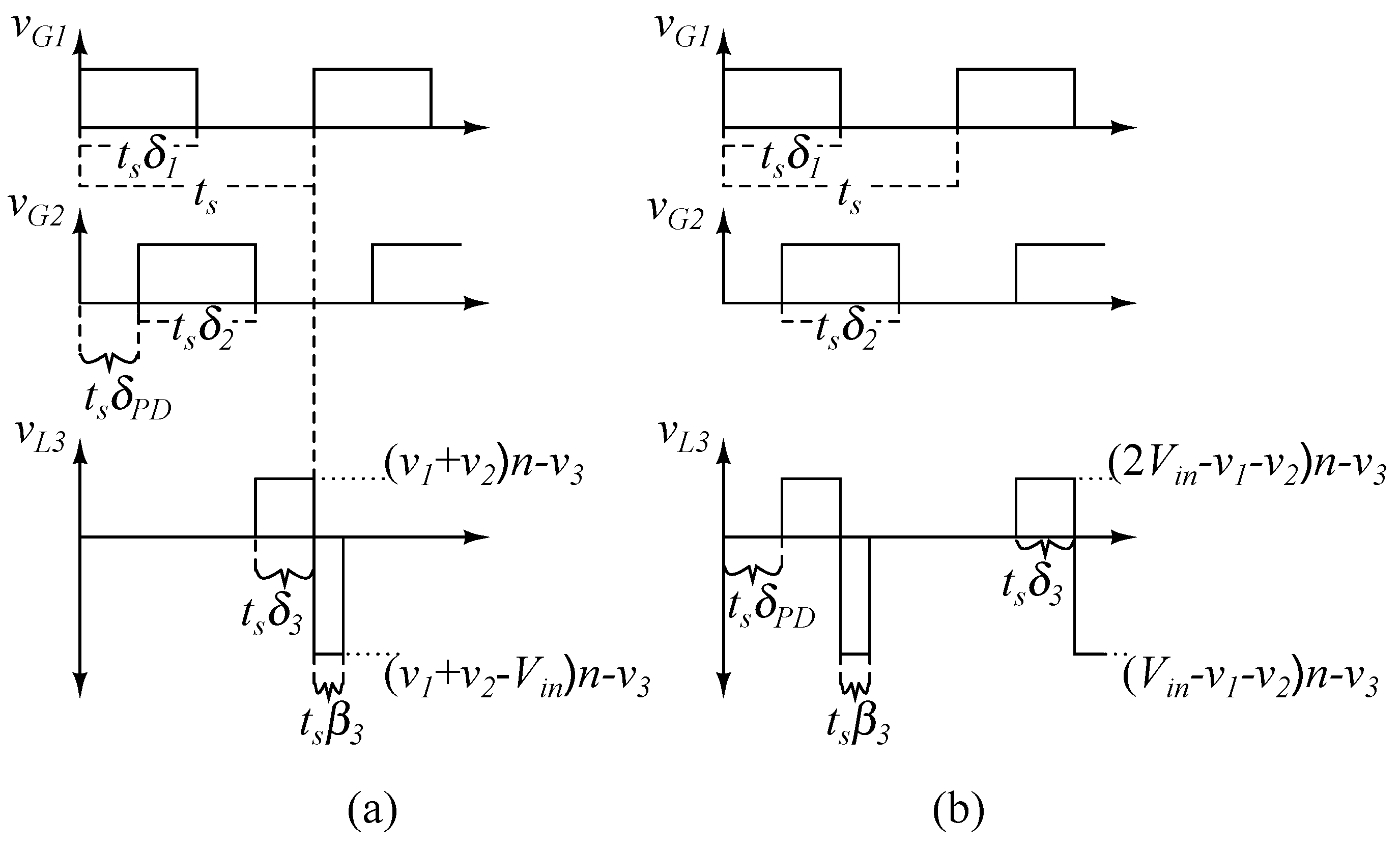
The gate voltage of the switches v and v, and the voltage waveform of the tertiary inductor, v of (a) a fly-buck type converter and (b) a forward-buck type three-output converter.
Figure 9.
The gate voltage of the switches v and v, and the voltage waveform of the tertiary inductor, v of (a) a fly-buck type converter and (b) a forward-buck type three-output converter.
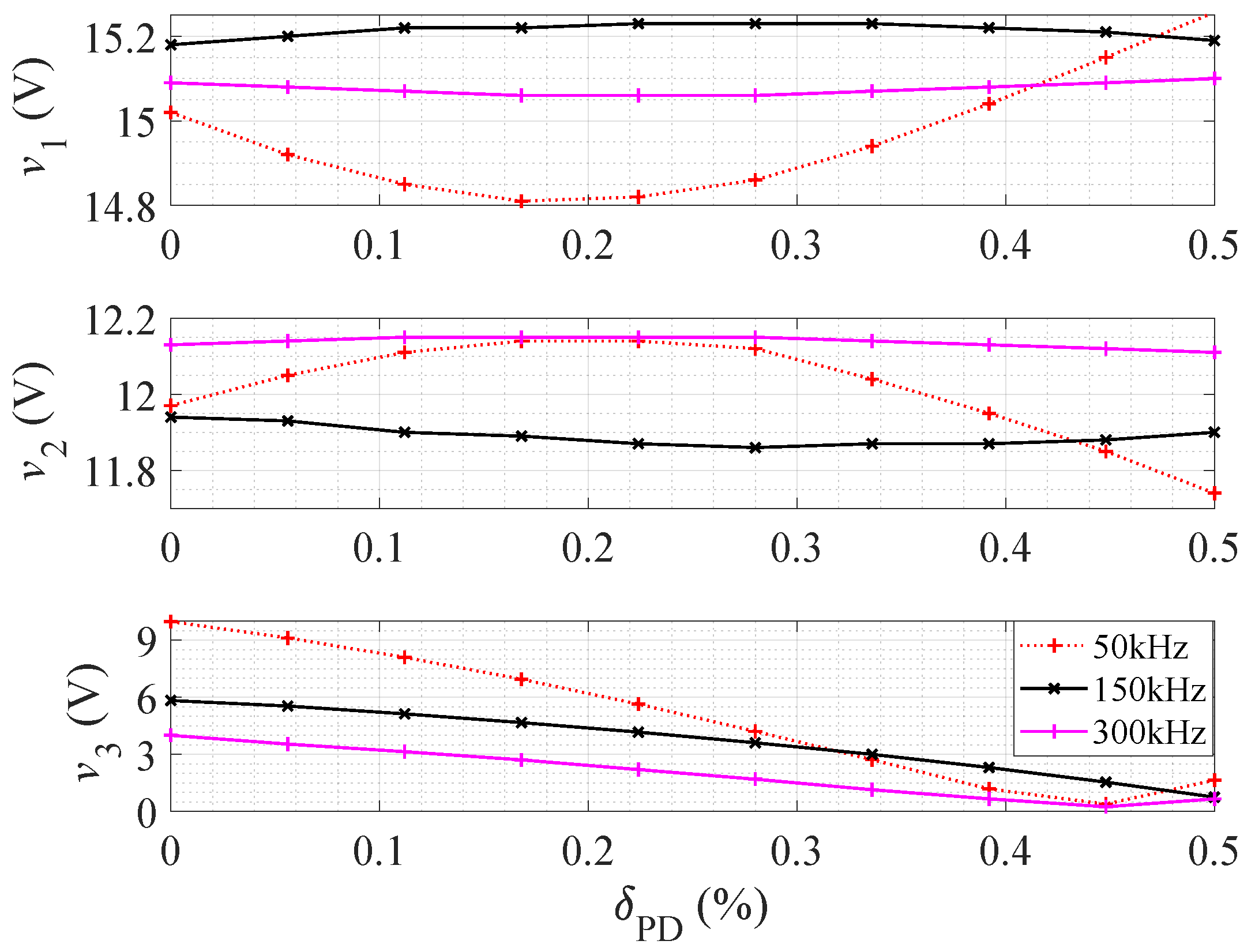
Figure 10.
Experimentally measured output voltages of the proposed fly-buck three-output converter, depending on different phase delays ( = 24 V, = 10 , = 8 and = 7.5 ).
Figure 10.
Experimentally measured output voltages of the proposed fly-buck three-output converter, depending on different phase delays ( = 24 V, = 10 , = 8 and = 7.5 ).
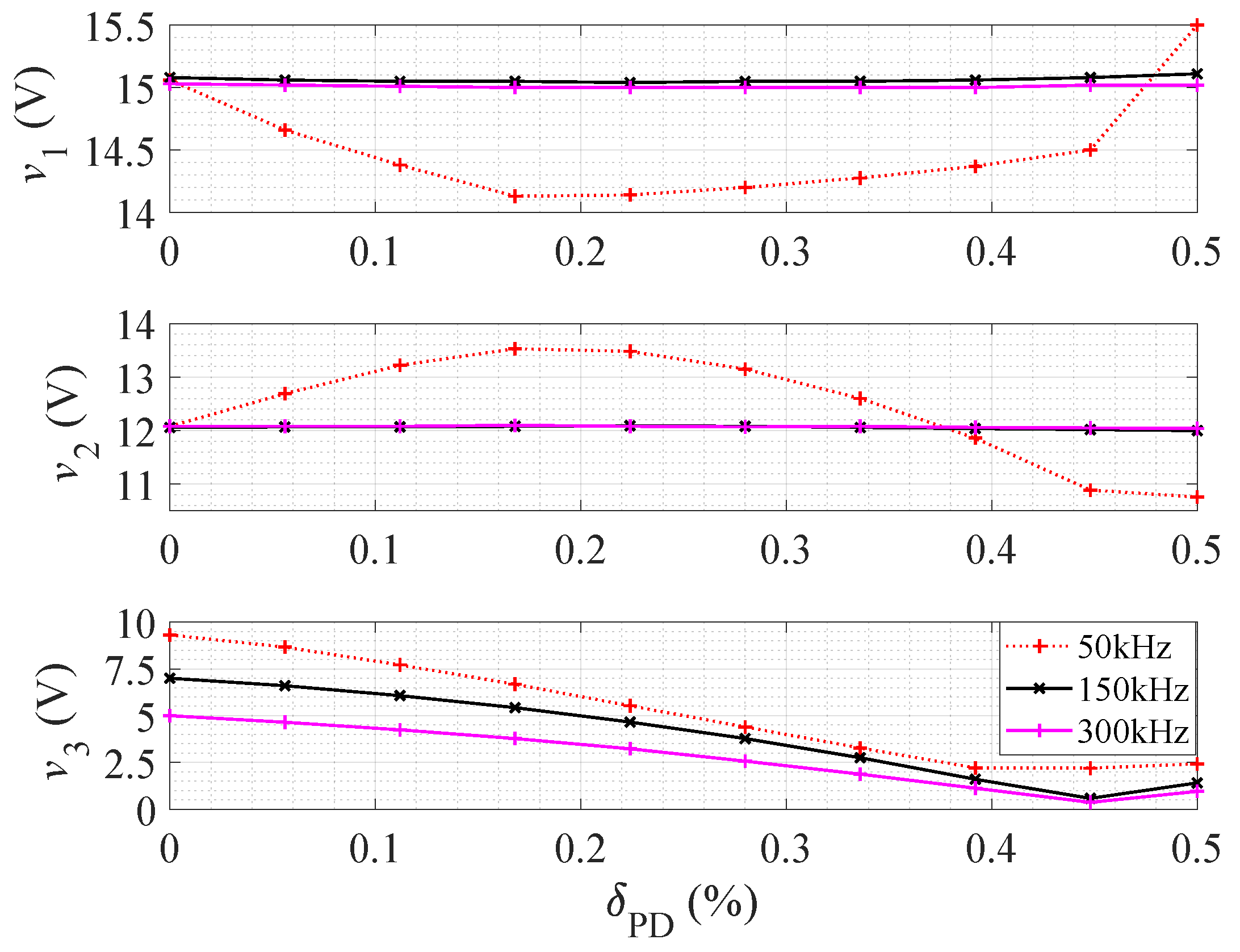
Figure 11.
Experimentally measured output voltages of the proposed forward-buck three-output converter depending on different phase delays ( = 24 V, = 10 , = 8 and = 7.5 ).
Figure 11.
Experimentally measured output voltages of the proposed forward-buck three-output converter depending on different phase delays ( = 24 V, = 10 , = 8 and = 7.5 ).
Figure 12.
(a) PWM-PFM-PD controlled five-output converter. Waveforms of gate voltages, current through the fourth inductor and the voltage across the fifth inductor when the fifth output is connected in (b) a fly-buck type and (c) forward-buck type converter.
Figure 12.
(a) PWM-PFM-PD controlled five-output converter. Waveforms of gate voltages, current through the fourth inductor and the voltage across the fifth inductor when the fifth output is connected in (b) a fly-buck type and (c) forward-buck type converter.
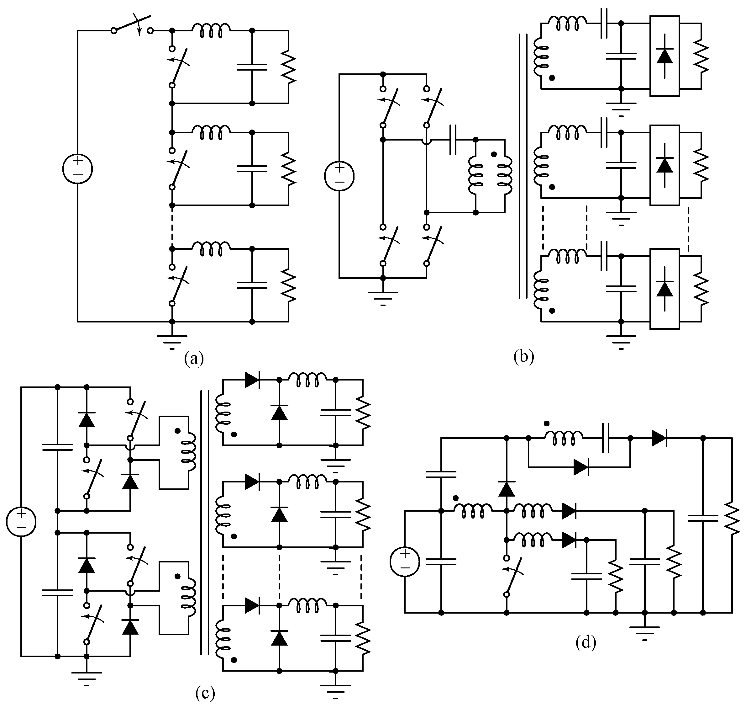
Figure 13.
Multiple-output dc-dc converters from the literature: which are (
a) an integrated multiple-output synchronous buck converter (IMOSBC) in [
22]; (
b) a multiple-output narrow-band resonant converter (MONBRC) in [
23]; (
c) a multiple-output two-transistor forward converter (MOTTFC) in [
24] and (
d) a single-input multiple-output dc-dc converter (SIMOC) in [
25].
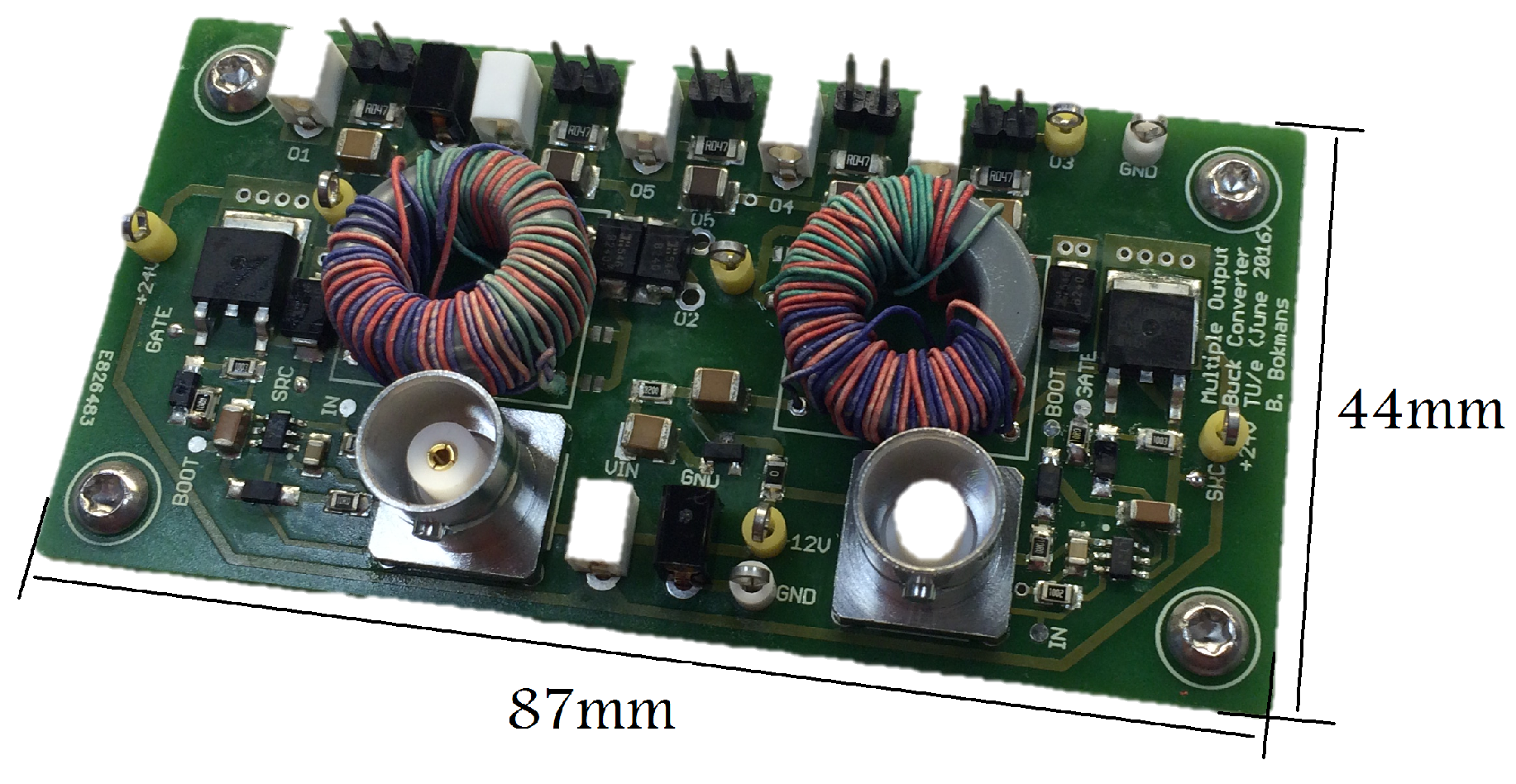
Figure 14.
Five output converter prototype.
Figure 14.
Five output converter prototype.
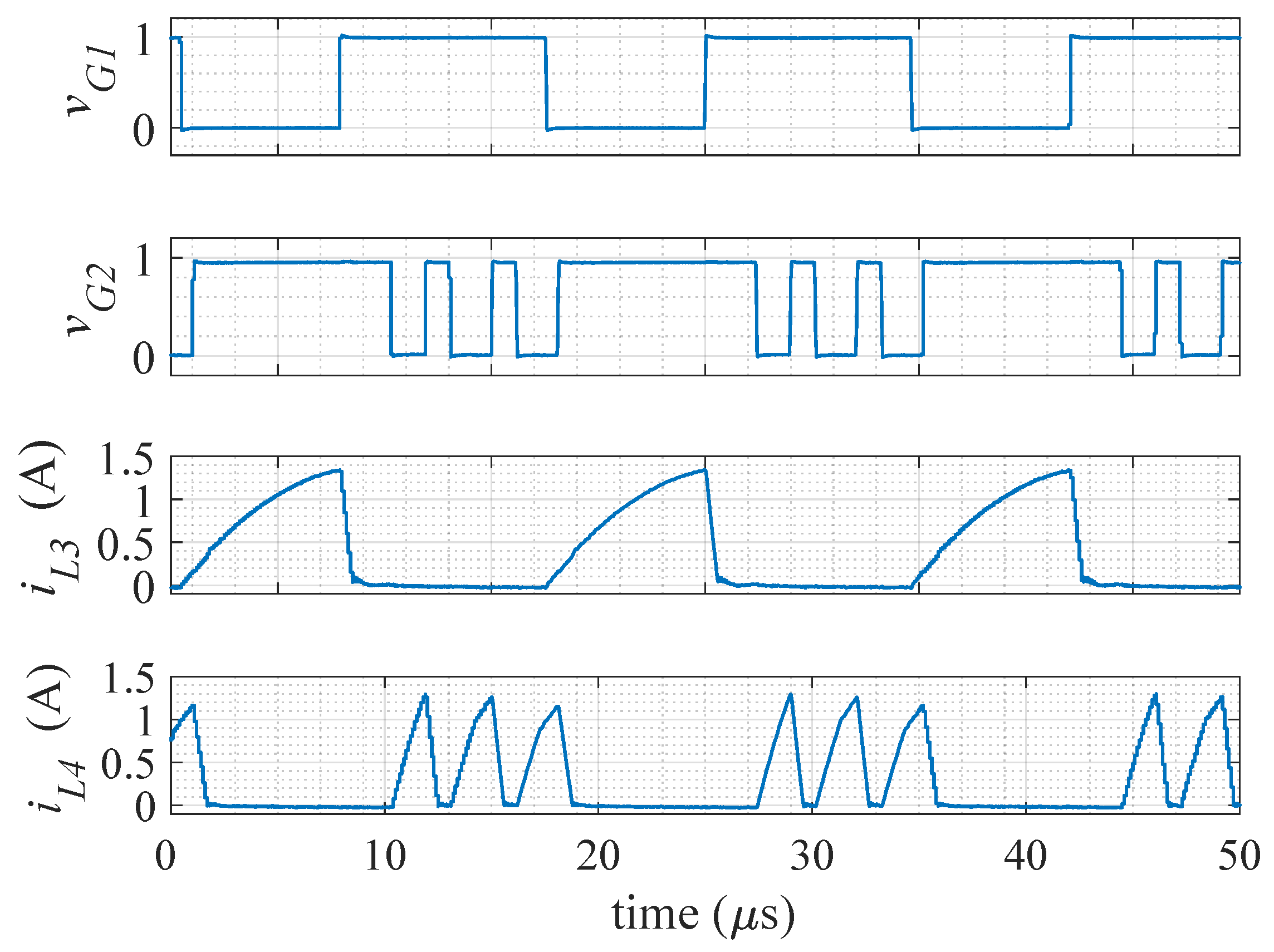
Figure 15.
Experimental waveforms of the gate voltages and , and current through the third and fourth leakage inductors when = 56.4%, = 57.3%, = 16%, f = 58.5 kHz and k = 3.
Figure 15.
Experimental waveforms of the gate voltages and , and current through the third and fourth leakage inductors when = 56.4%, = 57.3%, = 16%, f = 58.5 kHz and k = 3.
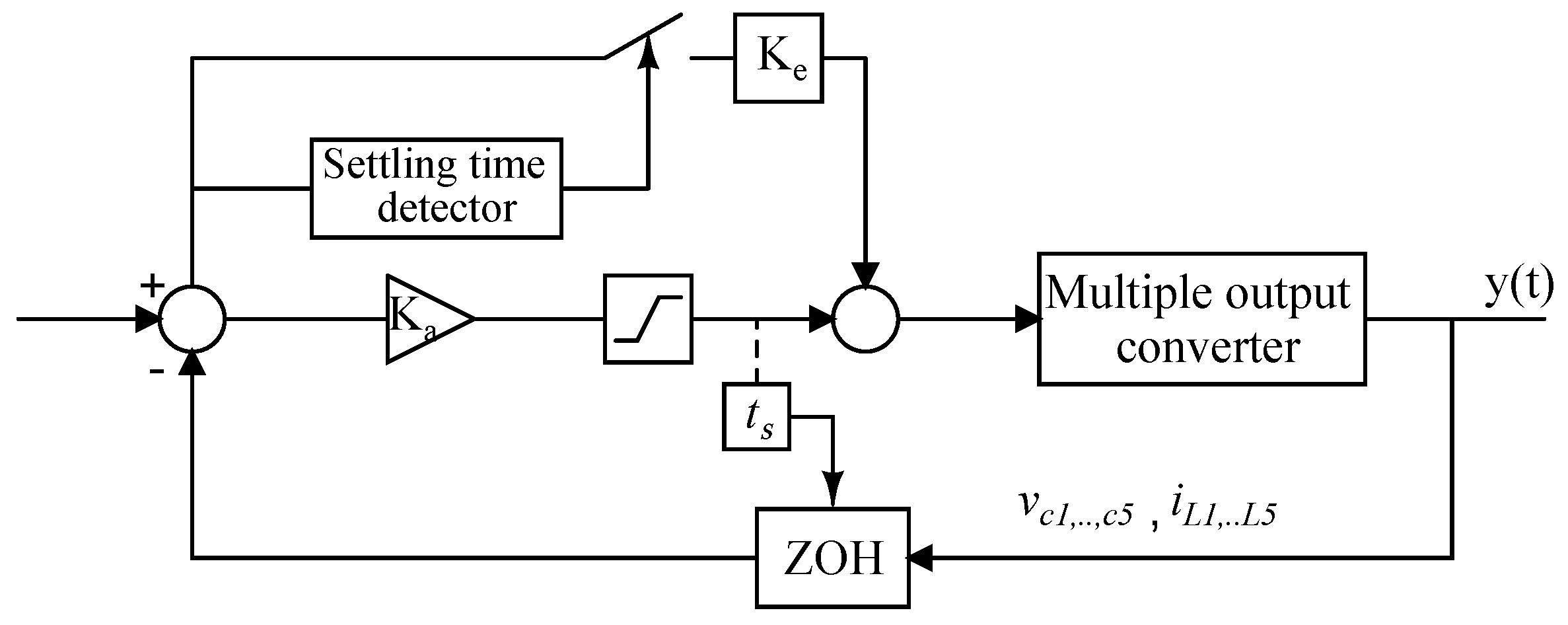
Figure 16.
Closed-loop block diagram of a state-feedback controller with error cancelation function.
Figure 16.
Closed-loop block diagram of a state-feedback controller with error cancelation function.
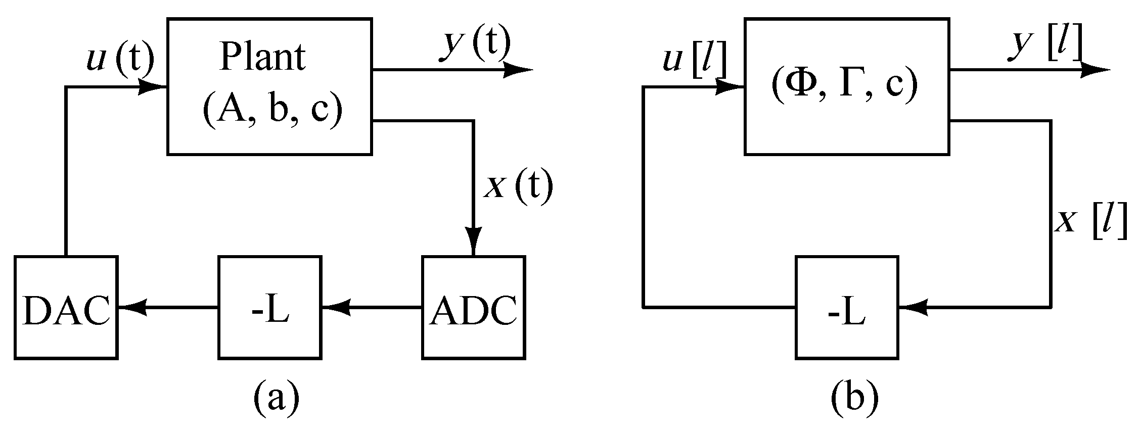
Figure 17.
(a) A regulation system using digital state feedback; (b) A zero-order hold (ZOH) design model for digital state feedback.
Figure 17.
(a) A regulation system using digital state feedback; (b) A zero-order hold (ZOH) design model for digital state feedback.
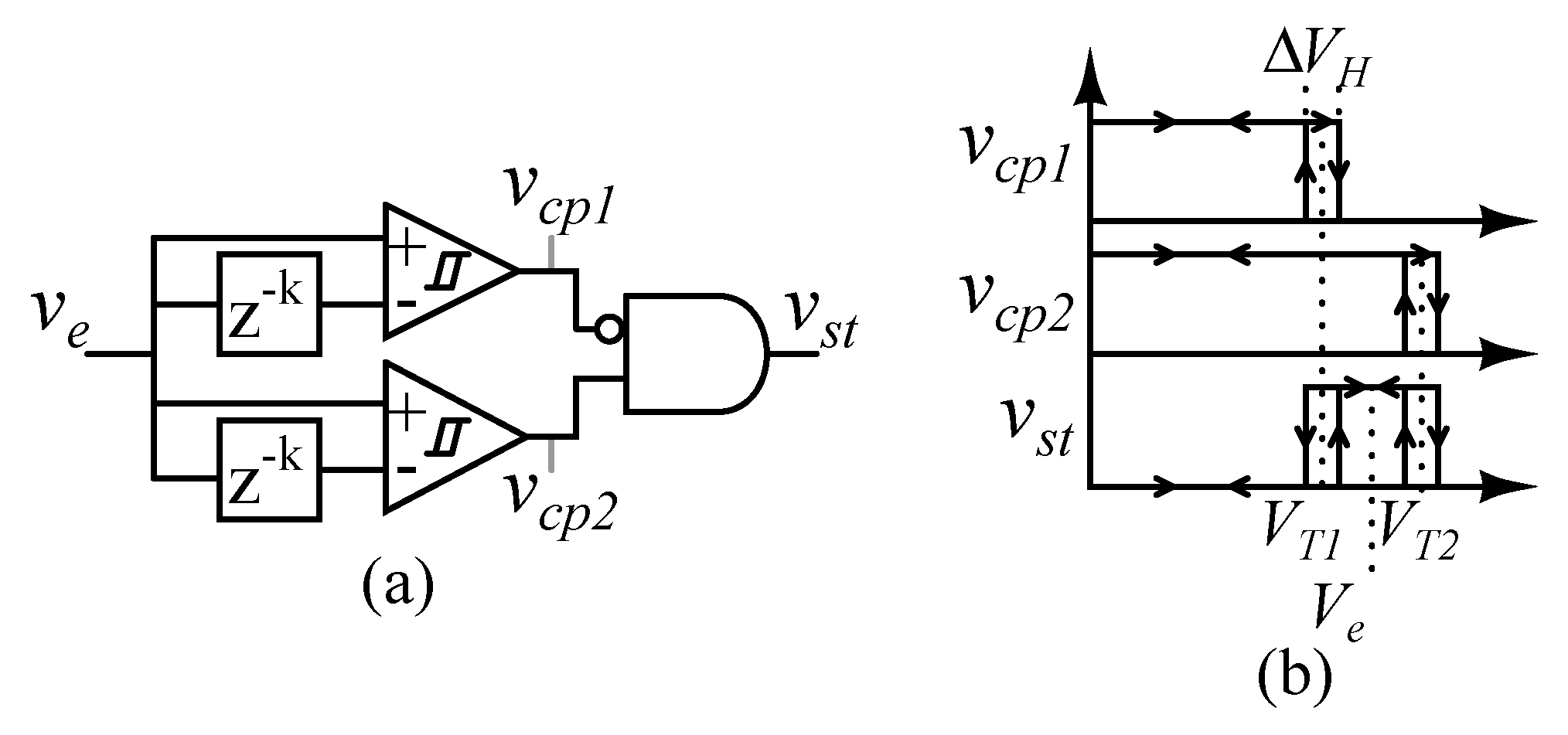
Figure 18.
(a) The block diagram of the detection circuit; (b) Output signals of the comparators and “and” gate as function of the delayed input signal.
Figure 18.
(a) The block diagram of the detection circuit; (b) Output signals of the comparators and “and” gate as function of the delayed input signal.
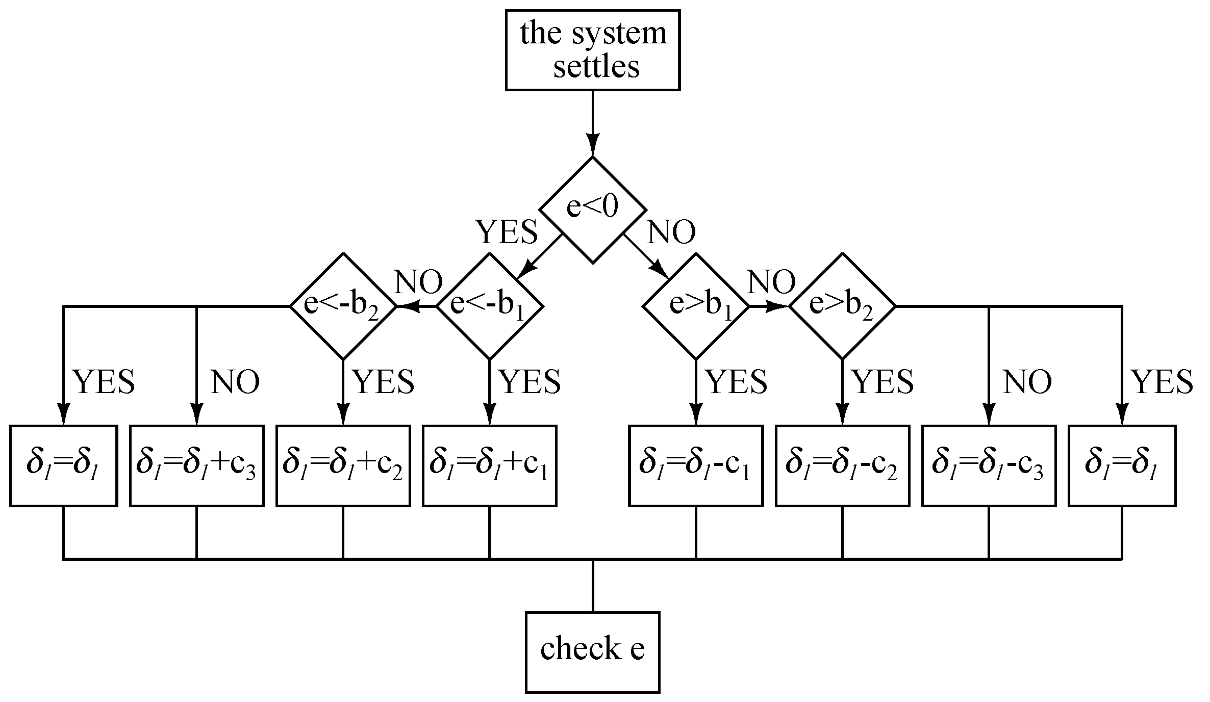
Figure 19.
Steady-state error(e) cancelation algorithm for the control parameter.
Figure 19.
Steady-state error(e) cancelation algorithm for the control parameter.
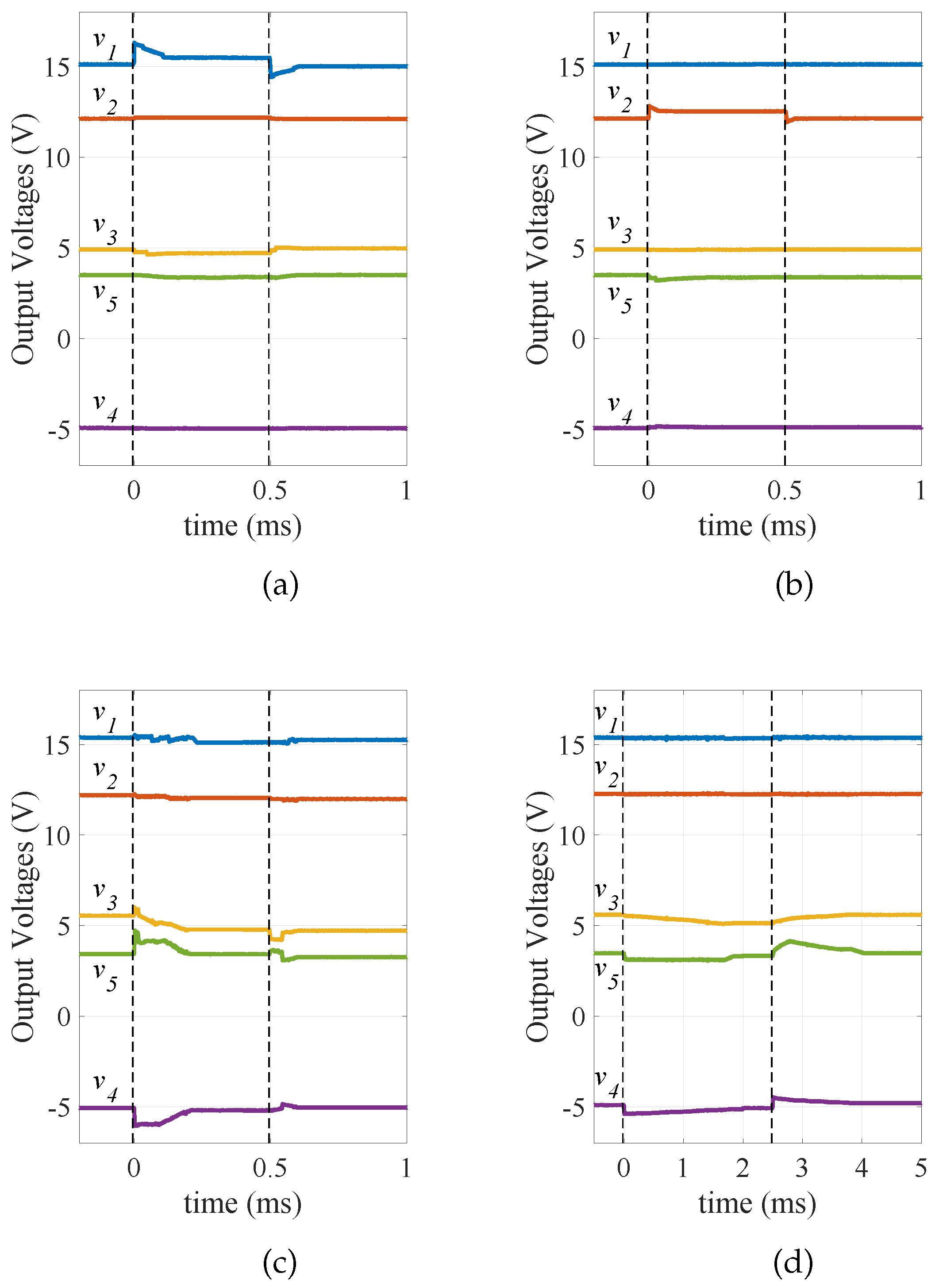
Figure 20.
Experimental results from the closed-loop five-output prototype: Output voltage responses (a) when the first output current changes from 1.5 A to 0.75 A, and from 0.75 A to 1.5 A; (b) when the second output current changes from 1.5 A to 1 A, and from 1 A to 1.5 A; (c) when the third output current changes from 0.8 A to 0.5 A, and from 0.5 A to 0.8 A; (d) when the fourth output current changes from 0.6 A to 0.4 A, and from 0.4 A to 0.6 A.
Figure 21.
Experimental results from the closed-loop five-output prototype: Output voltage responses (a) when the fifth output current changes from 0.45 A to 0.3 A, and from 0.3 A to 0.45 A; (b) when the input voltage changes from 21 A to 30 V, and from 30 V to 21 V.
Figure 21.
Experimental results from the closed-loop five-output prototype: Output voltage responses (a) when the fifth output current changes from 0.45 A to 0.3 A, and from 0.3 A to 0.45 A; (b) when the input voltage changes from 21 A to 30 V, and from 30 V to 21 V.
Table 1.
Components of the fly-buck and forward-buck two-output prototypes.
Table 1.
Components of the fly-buck and forward-buck two-output prototypes.
| Component | Value | Model |
|---|
| C | 2 × 22 F | TMK325B7226MM |
| C | 47 F | C1210C476M4PACTU |
| L | 150 H | produced in-house |
| | (turns ratio is 1/0.7) | |
| L | 3.5 H | |
| Q | | MTD3055VL |
| Gate Driver | | LTC4440 |
| D, D | | CD214B-B230LF |
Table 2.
Experimental results of the fly-buck converter (V = 24 V).
Table 2.
Experimental results of the fly-buck converter (V = 24 V).
| v (V) | v (V) | i (A) | i (A) | (%) | f (kHz) | (%) |
|---|
| 15.02 | 5.02 | 0.75 | 0.81 | 58.7 | 27.0 | 91.4 |
| 15.02 | 5.02 | 1.00 | 0.81 | 61.1 | 66.0 | 92.5 |
| 15.02 | 5.02 | 1.25 | 0.80 | 63.2 | 79.0 | 93.1 |
| 15.00 | 5.03 | 1.50 | 0.81 | 64.5 | 84.0 | 93.5 |
| 15.01 | 5.01 | 1.50 | 0.60 | 65.3 | 117.0 | 93.8 |
| 15.02 | 5.01 | 0.75 | 0.60 | 60.7 | 97.0 | 93.2 |
| 15.02 | 5.03 | 1.50 | 0.40 | 64.3 | 184.0 | 94.4 |
| 15.01 | 5.00 | 0.75 | 0.40 | 63.8 | 183.0 | 94.0 |
| 15.02 | 5.00 | 1.50 | 0.20 | 64.2 | 420.0 | 94.3 |
| 15.00 | 5.01 | 0.75 | 0.20 | 63.5 | 410.0 | 94.3 |
Table 3.
Experimental results of the forward-buck converter (V = 24 V).
Table 3.
Experimental results of the forward-buck converter (V = 24 V).
| v (V) | v (V) | i (A) | i (A) | (%) | f (kHz) | (%) |
|---|
| 12.02 | 5.06 | 0.754 | 0.610 | 51.9 | 45.0 | 91.7 |
| 12.06 | 5.01 | 1.000 | 0.605 | 52.5 | 45.0 | 91.7 |
| 12.03 | 5.03 | 1.252 | 0.606 | 53.1 | 40.0 | 91.9 |
| 12.02 | 5.00 | 1.518 | 0.602 | 53.6 | 40.0 | 91.6 |
| 12.02 | 5.01 | 1.502 | 0.300 | 52.9 | 97.0 | 93.1 |
| 12.07 | 5.01 | 0.751 | 0.300 | 51.8 | 110.0 | 93.3 |
| 12.03 | 5.01 | 1.503 | 0.101 | 52.7 | 380.0 | 93.3 |
| 12.03 | 5.00 | 0.748 | 0.101 | 51.2 | 470.0 | 92.9 |
Table 4.
Experimental results with a fly-buck type three-output converter (V = 24 V and f = 150 kHz).
Table 4.
Experimental results with a fly-buck type three-output converter (V = 24 V and f = 150 kHz).
| v (V) | v (V) | v (V) | i (A) | i (A) | i (A) | (%) | (%) | (%) | (%) |
|---|
| 15.00 | 12.02 | 3.32 | 1.498 | 1.498 | 0.442 | 65.4 | 52.7 | 20.5 | 94.4 |
| 15.00 | 12.01 | 3.30 | 1.498 | 1.497 | 0.309 | 65.4 | 52.7 | 24.3 | 94.7 |
| 15.01 | 12.01 | 3.30 | 1.498 | 1.496 | 0.152 | 65.4 | 52.7 | 28.6 | 95.1 |
| 15.01 | 12.00 | 3.30 | 1.499 | 1.496 | 0.074 | 65.4 | 52.7 | 30.7 | 95.1 |
| 15.04 | 12.03 | 3.31 | 0.753 | 0.750 | 0.077 | 64.2 | 51.6 | 31.2 | 95.3 |
| 15.02 | 12.03 | 3.30 | 0.252 | 0.252 | 0.078 | 63.0 | 50.6 | 31.9 | 92.6 |
| 15.25 | 12.12 | 3.30 | 0.256 | 0.253 | 0.300 | 55.5 | 33.6 | 7.7 | 91.9 |
Table 5.
Experimental results for a forward-buck type three-output converter (V = 24 V and f = 150 kHz).
Table 5.
Experimental results for a forward-buck type three-output converter (V = 24 V and f = 150 kHz).
| v (V) | v (V) | v (V) | i (A) | i (A) | i (A) | (%) | (%) | (%) | (%) |
|---|
| 14.99 | 12.07 | 3.30 | 1.512 | 1.500 | 0.456 | 65.5 | 53.0 | 14.4 | 94.4 |
| 14.99 | 12.07 | 3.31 | 1.511 | 1.500 | 0.303 | 65.5 | 53.0 | 23.1 | 94.7 |
| 14.99 | 12.05 | 3.31 | 1.512 | 1.500 | 0.150 | 65.5 | 53.0 | 32.2 | 94.9 |
| 15.02 | 12.02 | 3.31 | 1.516 | 1.491 | 0.075 | 65.5 | 53.0 | 47.5 | 94.9 |
| 15.00 | 12.10 | 3.30 | 0.751 | 0.751 | 0.075 | 64.1 | 52.0 | 38.9 | 95.1 |
| 15.02 | 12.04 | 3.30 | 0.252 | 0.250 | 0.307 | 63.0 | 50.7 | 23.1 | 90.7 |
| 15.02 | 12.06 | 3.30 | 0.251 | 0.250 | 0.075 | 63.0 | 50.8 | 38.0 | 92.1 |
Table 6.
Comparison of multiple-output converters.
Table 6.
Comparison of multiple-output converters.
| References | IMOSBC [22] | MONBRC [23] | MOTTFC [24] | SIMOC [25] | Proposed |
|---|
| Switches | 6 | 4 | 4 | 1 | 2 |
| Diodes | 0 | 20 | 12 | 5 | 5 |
| Magnetic components | 5 | 6 | 2 | 3 | 2 |
| Capacitors | 5 | 16 | 4 | 5 | 5 |
| Outputs | 5 | 5 | 4 | 3 | 5 |
Table 7.
Components of the five-output converter prototypes.
Table 7.
Components of the five-output converter prototypes.
| Component | Value | Model |
|---|
| C, C | 2 × 22 F | TMK325B7226MM |
| C, C, C | 47 F | C1210C476M4PACTU |
| L, L | 150 H | produced in-house |
| | (turns ratios are 1/0.7/0.7) | |
| L, L | 3.5 H | |
| L | 7.3 H | |
| Q, Q | | MTD3055VL |
| Gate Drivers | | LTC4440 |
| D, D, D, D, D | | CD214B-B230LF |
Table 8.
Experimental results for a five-output converter (V = 24 V).
Table 8.
Experimental results for a five-output converter (V = 24 V).
| | v (V) | v (V) | v (V) | v (V) | v (V) | i (A) | i (A) | i (A) | i (A) | i (A) |
|---|
| Case 1 | 15.17 | 12.11 | −5.08 | 4.76 | 3.28 | 1.54 | 1.54 | 0.81 | 0.57 | 0.45 |
| Case 2 | 15.09 | 11.99 | −5.00 | 4.74 | 3.30 | 0.75 | 0.98 | 0.50 | 0.39 | 0.30 |
| Case 3 | 15.04 | 12.13 | −4.91 | 5.28 | 3.32 | 0.76 | 1.53 | 0.65 | 0.79 | 0.31 |
| Case 4 | 15.15 | 12.10 | −4.80 | 4.76 | 3.37 | 1.52 | 1.03 | 0.58 | 0.77 | 0.48 |
| Case 5 | 15.12 | 12.13 | −4.98 | 5.13 | 3.39 | 1.52 | 1.54 | 0.41 | 0.80 | 0.47 |
| Case 6 | 15.00 | 11.96 | −5.06 | 5.38 | 3.30 | 1.50 | 1.49 | 0.62 | 0.61 | 0.45 |
| Case 7 | 15.16 | 12.10 | −5.00 | 5.16 | 3.40 | 1.54 | 1.56 | 0.60 | 0.80 | 0.31 |
Table 9.
The control parameters of a five-output converter at the operating points shown in
Table 8.
Table 9.
The control parameters of a five-output converter at the operating points shown in
Table 8.
| | (%) | (%) | (%) | (%) | f (kHz) | k |
|---|
| Case 1 | 92.9 | 67.28 | 54.70 | 11.84 | 85.5 | 3 |
| Case 2 | 93.5 | 64.67 | 52.07 | 15.46 | 129.5 | 3 |
| Case 3 | 92.5 | 59.40 | 53.78 | 7.04 | 66.3 | 2 |
| Case 4 | 92.7 | 66.26 | 51.80 | 13.57 | 51.0 | 5 |
| Case 5 | 93.0 | 65.91 | 54.53 | 9.91 | 69.7 | 5 |
| Case 6 | 92.6 | 64.89 | 53.20 | 10.37 | 88.5 | 2 |
| Case 7 | 92.9 | 66.84 | 55.10 | 3.12 | 65.2 | 3 |
Table 10.
Charging capacitors over the entire period using an inductor operating in DCM.
Table 10.
Charging capacitors over the entire period using an inductor operating in DCM.
| SSA Equivalent | Actual Equivalent |
|---|
| Charging Current | Charging Current |
|---|
| |
| |
| |


