1. Introduction
In the IoT era, the ubiquitous use of sensitive and private data requires reliable and secure embedded systems where a reasonable amount of memory is required for security code encryption or key storage. This sensitive data is commonly stored in embedded non-volatile memories (NVMs) such as ROM, e-fuse (electronic-fuse) or anti-fuse, battery- backed SRAMs or logic EEPROM/Flash. Masked ROM memories store keys during manufacturing. Therefore, a change in the key requires modifying the mask layout. E-fuse [
1] and anti-fuse [
2,
3] are one-time programmable (OTP) memories, which can be built in a generic digital process, but the programming operation is irreversible. A battery-backed SRAM is a power-gated SRAM in data retention mode. The battery is required to avoid the volatility of SRAM memories, at the expense of an increase in cost, complexity, and power consumption. Logic EEPROM/Flash [
4,
5,
6] are based on the floating gate technology and have been successfully deployed in automotive microcontroller units (MCU) and smartcard ICs. However, they are still expensive and require additional masks and process steps in comparison with the standard CMOS technology. All these NVMs present the same security vulnerability, since data remain in the memory even without power, exposing it to potential attackers. Confidentiality attacks aim at extracting this stored information. In the case of NVMs, attackers aiming at stealing private data can succeed in their objective with the aid of cold-boot attacks or other removal strategies like stealing memory modules [
7,
8]. As an alternative, secret keys can also be extracted from security primitives, the so-called physical unclonable functions (PUFs) [
9]. PUFs are physical structures that embrace manufacturing variations resulting from the IC fabrication process to generate a key. Although PUFs provide a promising alternative for a key generation [
10], they still pose challenges like low reliability, need for error detection and area overhead.
In this context, resistive random access memories (RRAMs) have emerged as a promising alternative to replace current memories [
11,
12]. Moreover, the inherent variability of RRAMs, due to the stochastic nature of their switching mechanism [
13], has positioned these devices as one of the most competitive candidates for the development of security primitives [
14]. In fact, RRAMs have attracted the attention of the research community for the implementation of PUFs [
15,
16,
17,
18,
19,
20,
21,
22,
23] and true random number generators (TRNGs) [
24,
25,
26,
27,
28,
29]. Nevertheless, RRAM-based circuits may also introduce security vulnerabilities of their own. One of the main concerns is related to its inherent non-volatility, since data written to the memory persist even when the system is powered off, arising a similar problem as present NVMs. This fact may expose RRAMs to a variety of physical attacks, compromising data confidentiality [
30]. For this reason, extensive effort is currently devoted to improving the security of RRAM-based memories. These approaches propose security improvements at the physical or circuit level [
31,
32,
33,
34] and at the authentication or encryption level [
35,
36]. However, all these proposed approaches still do not address the fundamental problem of privacy data remaining in memory after the power is turned off.
The present paper proposes the association of two RRAMs in a serial configuration as a basic cell for secure NVMs, which could solve this critical problem. This cell has already been proposed for other security applications [
25,
37,
38]. However, unlike these previous works, in this paper the cell is excited in such a way that the deterministic switch of one of the RRAMs is obtained. The configurations of the cell where both devices are in different resistance states are leveraged to store one bit of information. The operation of the cell provides also the capability of masking and unmasking the data on demand. With this countermeasure the protection against physical attacks is enhanced when the device is powered off or when the sensitive data is not used. Furthermore, side-channel attacks that conduct information stealing by monitoring the current consumption are preventable in this work. The presented experimental results are a proof of concept that validates the applicability of the proposed cell. Moreover, a potential array architecture based on the serial RRAMs memory cell is proposed and its ability to defend the physical attacks is discussed.
The rest of the work is organized as follows. A short review about the use of RRAM devices as memory cells and related security aspects is found in
Section 2. The serial RRAM memory cell and its functionality details are presented in
Section 3. Next, experimental results are summarized in
Section 4. An array architecture proposal based on the serial RRAM cell is found in
Section 5. The security features arising from the cell and the proposed array architecture are discussed in
Section 6. Finally, the conclusions are drawn in
Section 7.
2. RRAM Cell and Security Aspects
RRAMs are devices belonging to the memristor type [
39] and are typically composed of an electrode/dielectric/electrode stack structure. Its resistive switching mechanism relies on the formation and rupture of conductive filament (CF) based on defects in the oxide (dielectric) between the two metal electrodes [
11]. For a RRAM in a pristine state an initial operation, called the forming process, is usually required to generate the CF. Once the CF is formed, a RRAM can reversibly switch between a high resistance state (HRS) and a low resistance state (LRS). This switching behavior is obtained by applying voltage pulses between the electrodes in a bipolar mode for most of the existing technologies [
40]. Furthermore, when the voltage is removed, RRAM would memorize the current resistance state until the next voltage is applied and the resistance state can be maintained for several days or even years [
41]. The switching operation from HRS to LRS is called the SET process, whereas the switching operation from LRS to HRS is called the RESET process. The non-volatility properties of RRAMs have motivated their use as memory devices, although other fields such as digital logic, analog circuits, neural networks, and hardware security are also receiving considerable attention.
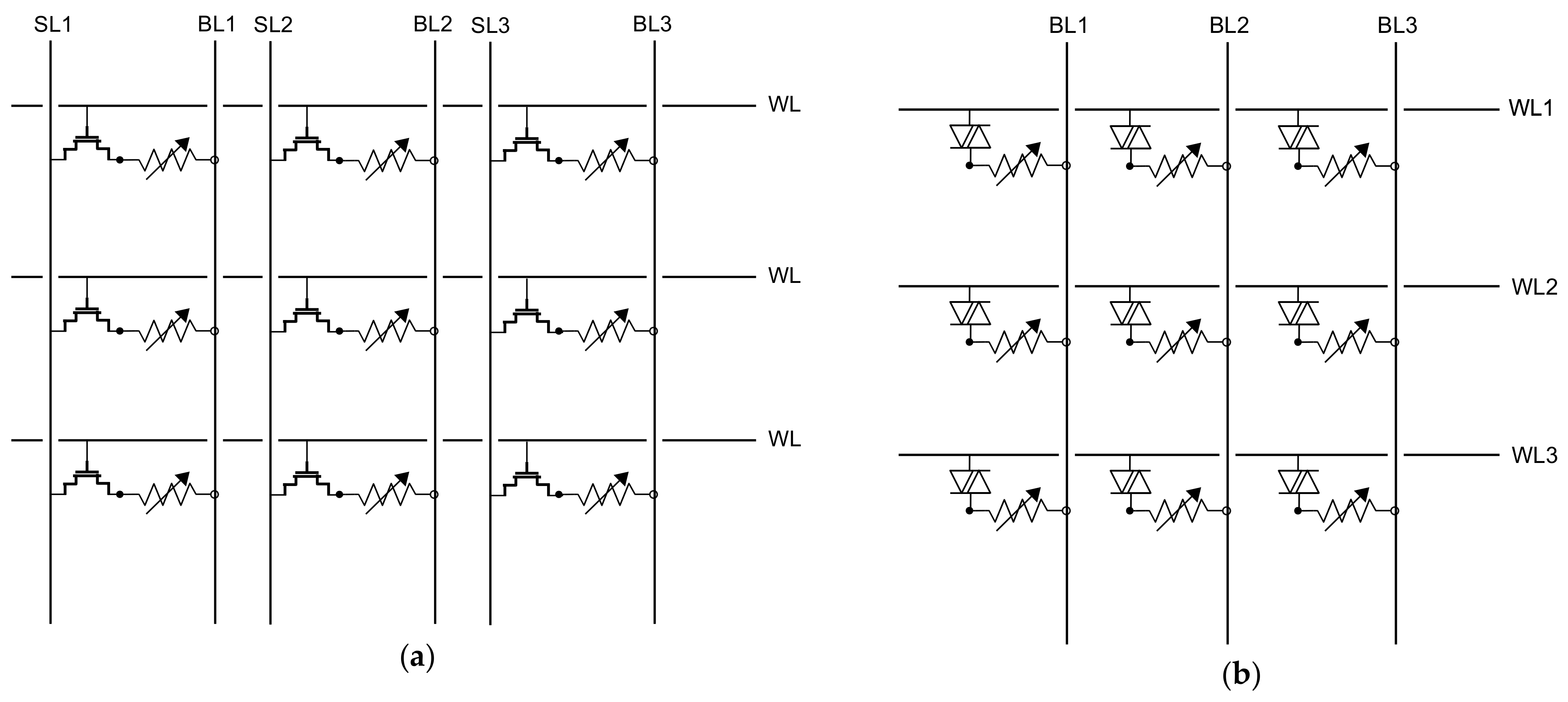
Concerning memory applications, there are mainly two array architectures for RRAM integration [
42]: 1T1R and cross-point array. The former offers better write/read margins and has a bigger array size whereas the latter shows smaller cell area and lower power consumption. Furthermore, cross-point arrays typically include selectors (one-selector and one-resistor (1S1R) architecture) to prevent interference between cells and avoid the sneak-path issue.
Figure 1a shows the typical scheme for the 1T1R array. The RRAM is in series with a cell selection transistor, which isolates the selected cell from other unselected cells. The word line (WL) controls the gate of the transistor. Therefore, tuning the WL voltage allows the control of the write current that is delivered to the cell. In
Figure 1b, a crossbar array based on a 1S1R cell is shown. Each RRAM is connected at the cross-point between a word-line and a bit-line. A selector (two anti-parallel diodes-like device) is connected in series in order to minimize the sneak current effect. By applying positive or negative writing voltages to lines WL and BL, each RRAM can be switched to
or
thus storing a ‘1’ or ‘0’ bit.
Memories storing sensitive information are usually protected by encrypting their content. However, for certain setups, keys need to be written in plaintext. A practical case can be seen in the Lohrke et al. paper for a real
Xilinx-FPGA [
43]. It becomes, then, important to have memories that are secure at the hardware level, in which the bits become self-protected against possible adversary attacks.
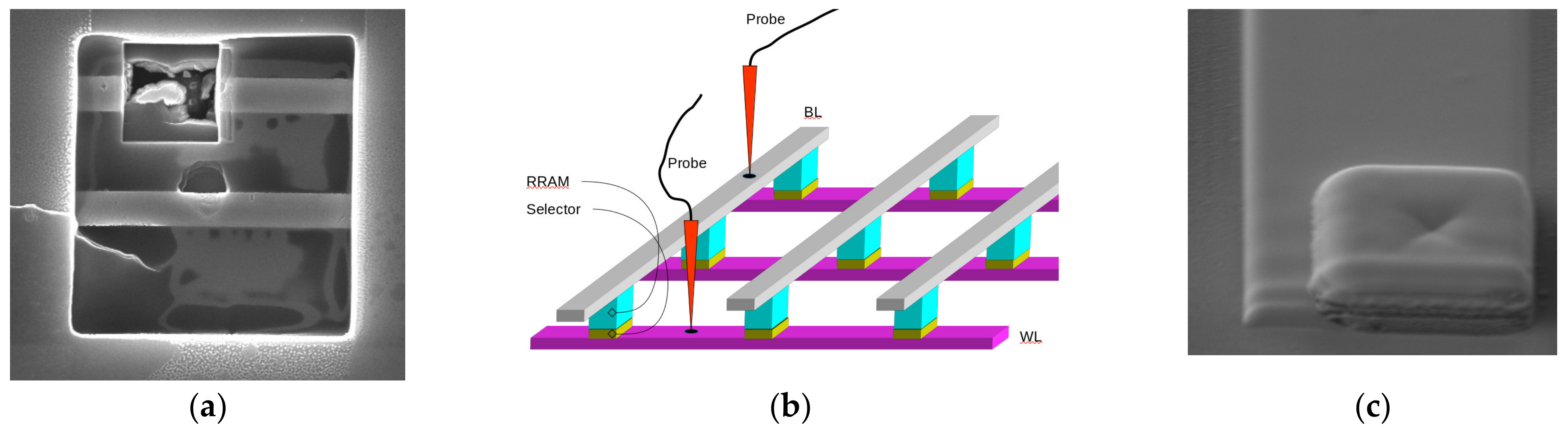
The RRAM-based technology is compatible with CMOS fabrication and is added at a backend process module. RRAMs layers are placed in the most external part of the chip in which the cross-point structures can be found [
44]. From this, one immediate vulnerability can be identified by adversaries, who are able to apply reverse engineering techniques. As it is shown in
Figure 2a, FIB equipment can be used to open access at row and column metal lines and to pin probes. From these, RRAM resistances can then be passively measured and bits are extracted. In
Figure 2b a drawing illustrating this attack is shown and in
Figure 2c it can be seen how probes can be pinned. Usually, the probes themselves cannot contact the lower layers through the opens but metallizations are added which bring the connections to the surface. This type of attack is usually prevented by adding protecting shields (active or passive). Anyhow, these shields are expensive and consume, at least, a full metallization layer [
45].
A second vulnerability exists during the reading of the cells. When a word line is activated, a set of RRAMs are biased with the reading voltage and the flowing current is sensed. The accumulated current becomes an image of the number of 1 s and 0 s that exist at this particular word, becoming correlated to the hamming weight. This kind of leakage is usually exploited by adversaries to revert keys from security chips using side-channel attack techniques. In this context, the improvement of security features of RRAM-based memories has become a topic of extensive research.
3. Serial RRAM Cell for Secure NVMs
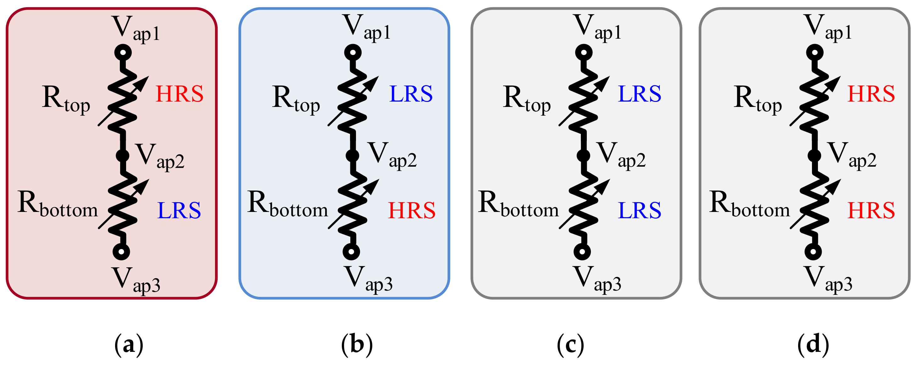
The considered serial RRAM memory cell is a kind of differential cell in which bits can be concealed. As shown in
Figure 3, it consists of two RRAMs connected in series. Four different cell states can be identified from the two possible resistance states of each RRAM, see
Figure 4:
‘0’,
‘1’,
,
. The behavior of the cell is as follows: with the two RRAMs initially in the
, during a serial RESET (SRESET), i.e., a RESET operation of the two serially connected devices, one of the RRAMs switches to the
HRS first. When the SRESET is initiated, the voltage across the switching device increases, preventing the other device to switch. During a subsequent serial SET (SSET), i.e., a SET operation of the two serially connected devices, only the RRAM in the
switches back to the
, since the other one is already in the
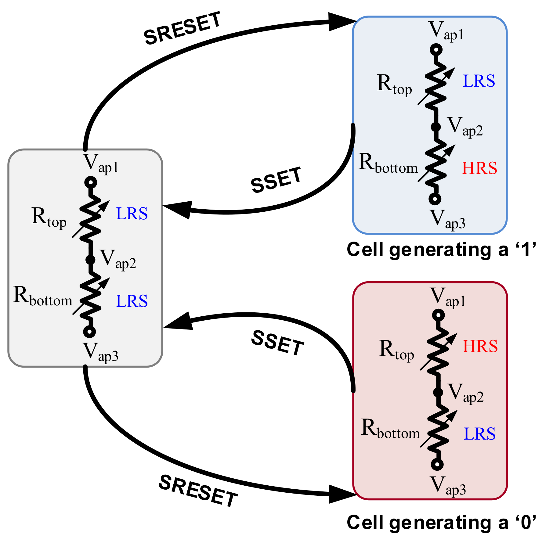
. For subsequent SSET and SRESET the switching device is always the same. The basic operation of the cell is reported in
Figure 5. Furthermore, considering the unused configuration in which both RRAMs are masked in the HRS, one of the RRAMs switches first to the LRS in the subsequent SSET operation, which raises the voltage across the other non-switching RRAM device, forcing it to switch to the LRS as well. In this case, both devices may end up in the LRS if the SSET voltage is not withdrawn in time, compromising the functionality of the cell. That is the main reason why this configuration (HRS, HRS) is not adopted here. Given a particular pair of devices initially in the LRS, by applying consecutive SRESET and SSET operations the bit can be unmasked and masked, respectively. Depending on which of the RRAMs switches to the
after a SRESET, two different states of the cell can be differentiated (the so-called ‘0’ or ‘1’). The RRAM that goes first to the
depends on device-to-device variability. Therefore, every cell generates an unpredictable bit, which is maintained during subsequent SRESET and SSET operations. Furthermore, it adds masking capability since both devices remain in the
after a SSET. This fact can be exploited to generate unpredictable bits with the potential application in PUFs [
38].
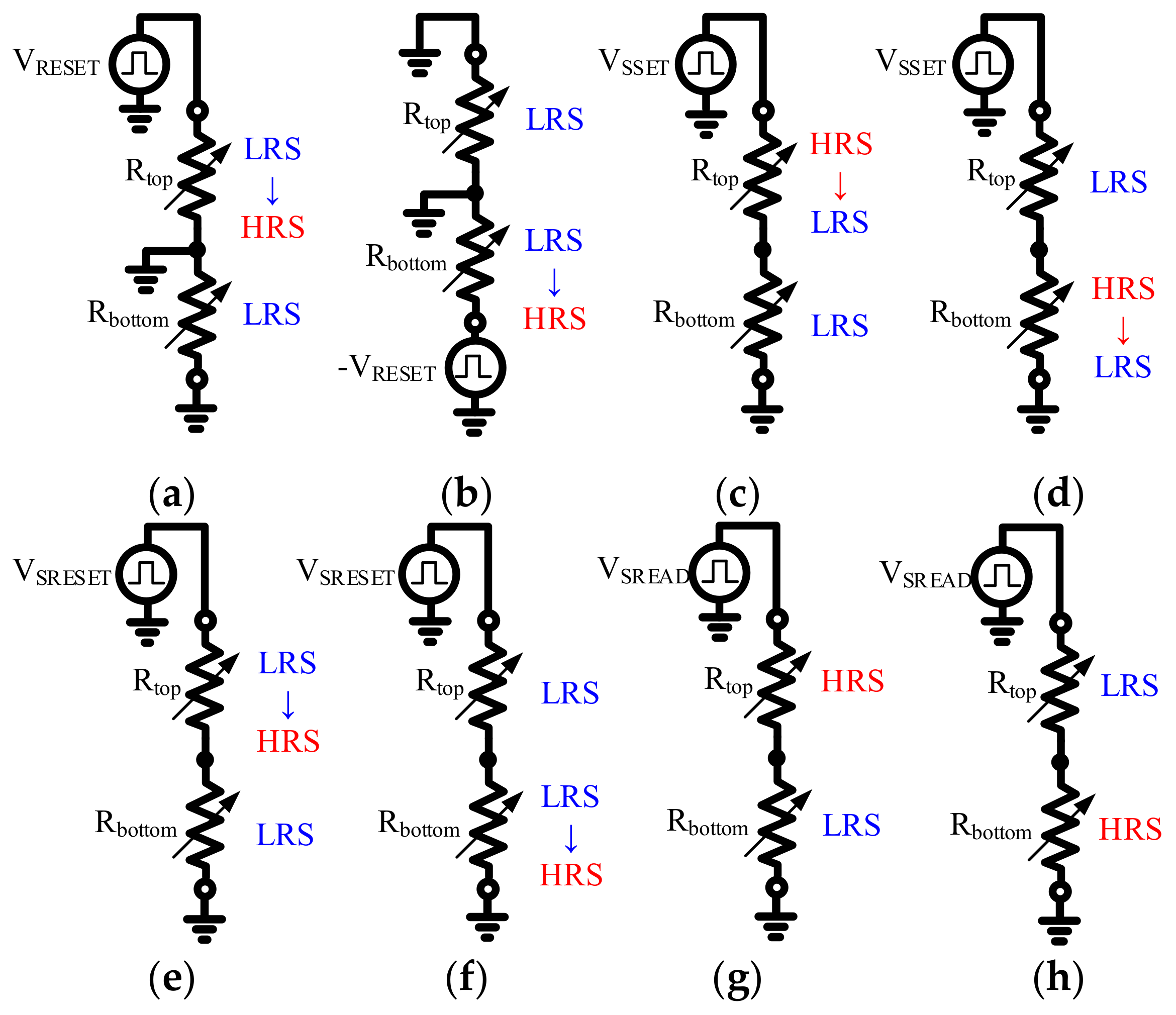
This serial RRAM cell is proposed in the present work for secure NVMs. However, for this application, we must include writing capabilities to obtain a full operational memory cell. This fact requires the capability of writing data to the cell while maintaining the feature of masking/unmasking the bit. For this purpose, during the write operation, individual SET and RESET operations are applied so that the middle node
is grounded and nodes
and
are biased accordingly, as illustrated in
Figure 6a,b for write-0 and write-1 operations, respectively. During masking and unmasking operations the middle node
is left floating and voltages at nodes
and
are applied accordingly. The masking operation is performed by bringing the two RRAMs to
with a SSET, which forces the same current passing through both devices, see
Figure 6c,d. After this operation, it is arduous to know what the previous combination of states
or
was. However, if an unmasking operation (SRESET) is applied (forcing the same current through both devices) the previous state
or
is restored, see
Figure 6e,f. With the cell in an unmasked state, a read operation (SREAD) is conducted, as illustrated in
Figure 6g,h. Node
is grounded and the read voltage is applied to node
while the voltage at the floating node
is measured and compared to a reference voltage to read the bit. The complete behavior of the cell is demonstrated next.
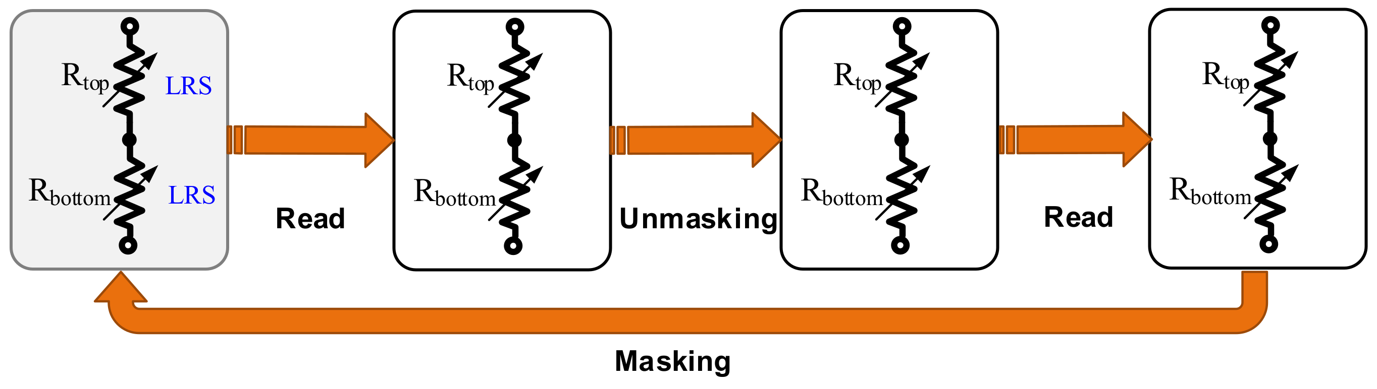
According to the different configurations of the cell reported in
Figure 6, a full operation of the cell can be derived, as the sequence of operations illustrated in
Figure 7. Starting from both devices in the
, a write operation is applied to the cell to store the secret bit (write-0 in
Figure 7a and write-1 in
Figure 7b). Subsequently, a masking operation is applied to conceal the bit. Then, the secret can be revealed on demand by applying an unmasking operation followed by a read operation. Once the information has been obtained, the secret is masked again. This sequence of operations (unmasking-read-masking) can be applied as many times as needed. In this way, the information is only exposed in a small fraction of time when it is used, remaining secured during the rest of the time, even when the system is powered off.
4. Experimental Results
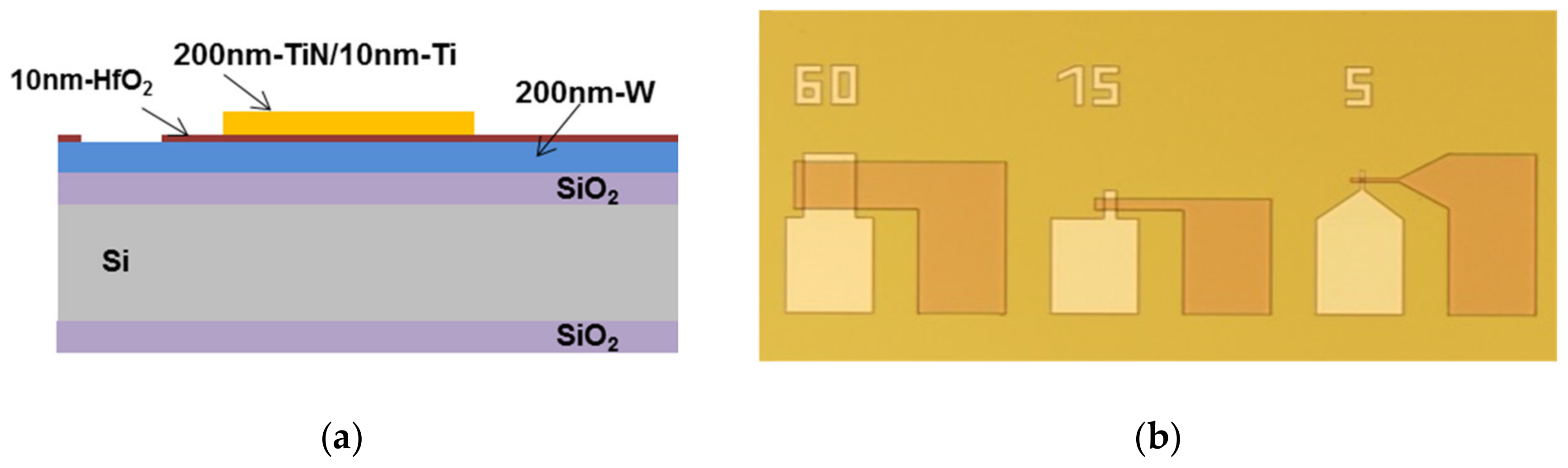
Experiments were conducted to assess the feasibility of the proposed cell. The RRAM devices used in the experiments are TiN/Ti/HfO
2/W structures [
20,
38].
Figure 8a shows a schematic cross-section of the final device structure. A top view optical microscope image of the structures is illustrated in
Figure 8b, which are square cells of 60 × 60 μm
2, 15 × 15 μm
2 and 5 × 5 μm
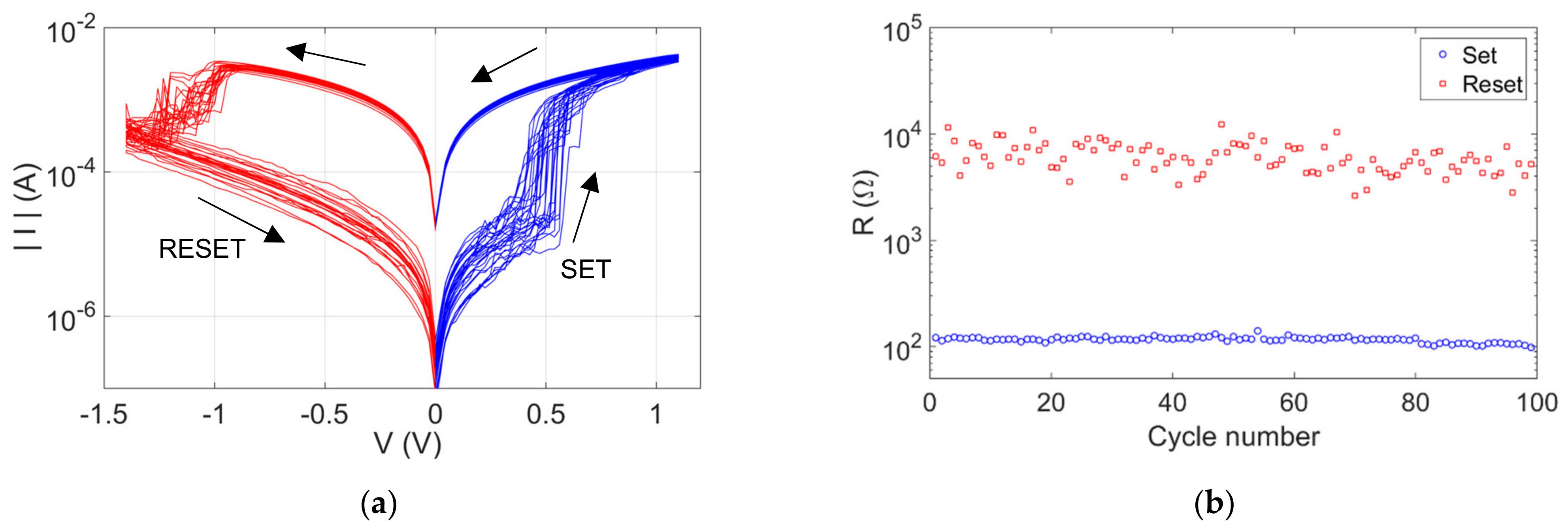
2. The electrical characterization of the devices was performed using two synchronized B2912A precision source/measure units (SMUs, Keysight, Santa Rosa, CA, USA). The typical resistive switching characteristics under DC conditions are shown in
Figure 9a, where double-sweep voltage ramps were applied from 0 V to +1.1 V for the SET, and from 0 V to −1.4 V for the RESET operations. The corresponding cycling behavior under the pulse mode, using the same voltage amplitudes as those in DC conditions, is presented in
Figure 9b.
The pulse mode was assessed and before checking the functionality as a memory cell, an initial experiment was performed to reproduce the results in [
38]. It consisted in starting from both devices in the LRS, applying a sequence of unmasking-masking operations (both followed by a read operation) without forcing a write operation in advance, as illustrated in
Figure 10. Which of the devices is going to switch after the first unmasking operation is unpredictable, but for subsequent masking/unmasking operations, the switching device is expected to be the same. Depending on which of the RRAMs switches to the
two different states of the cell (‘0’ or ‘1’) can be differentiated, as previously presented in
Figure 4a,b. Experimental results for a serial cell are shown in
Figure 11a,b, which were derived from the read operations after masking and unmasking, respectively. In this example,
switches to the
, whereas
remains at the
. Considering the results in
Figure 11b, and according to the definitions in
Figure 4, ‘1’ was stored in this example. However,
Figure 11a shows that the bit (‘1’ in this particular example) is masked after a SSET since both devices remain in the
. The RRAM that goes first to the
depends on the
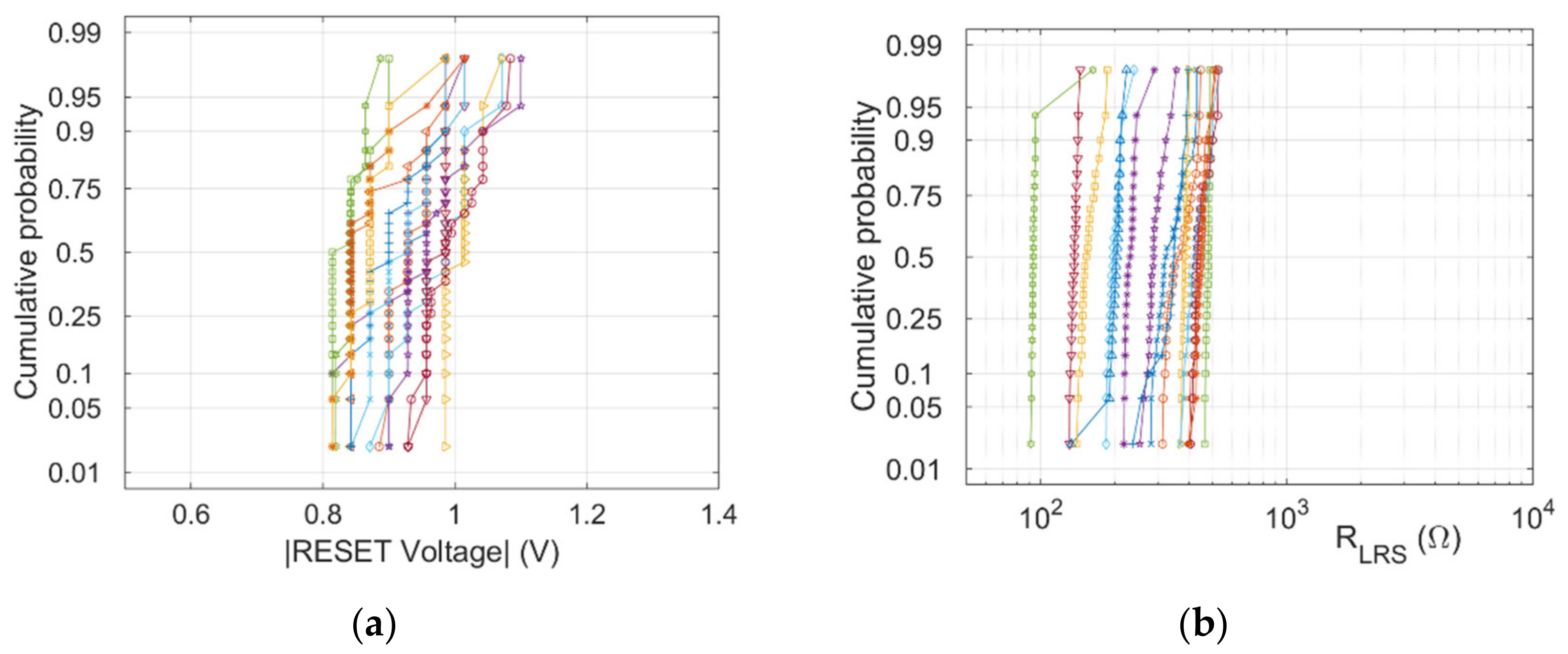
resistance and the RESET voltage of the devices in every particular cell. This persistent behavior is mainly due to the higher inter-device variability as compared to the intra-device variability, as shown in
Figure 12a for the RESET voltage (
) and in
Figure 12b for the resistance in the
(
). The data was derived from 25 DC cycles of 15 different devices.
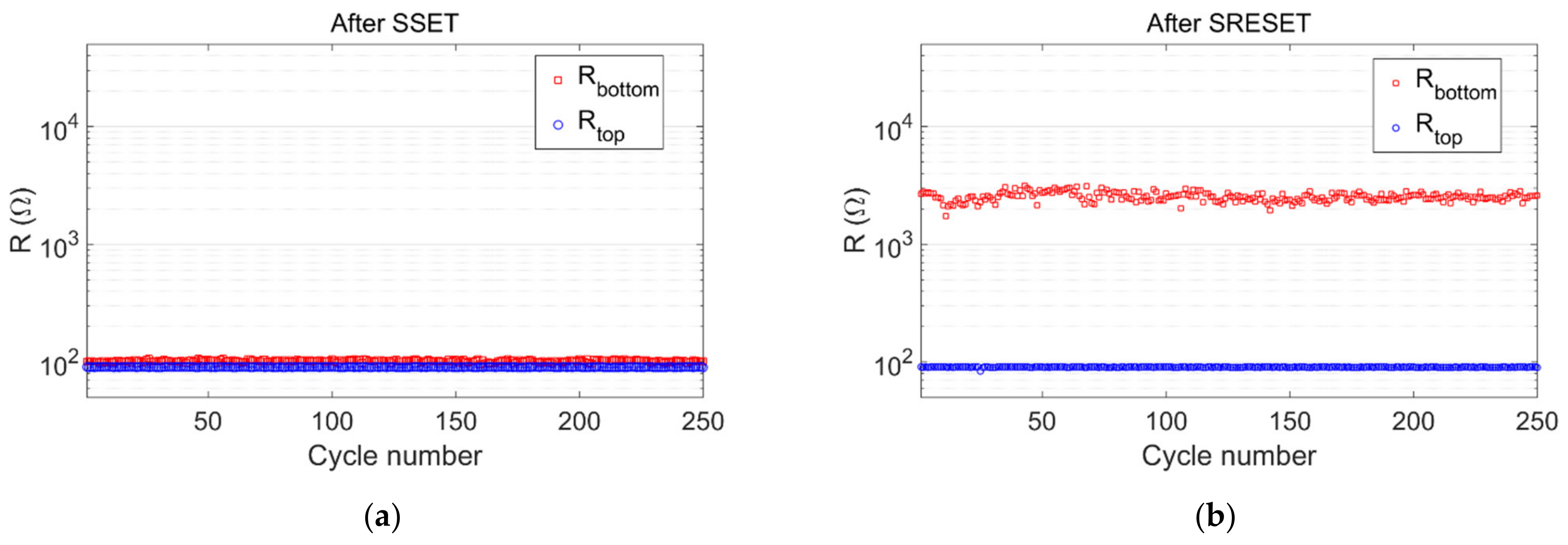
The experimental set-up was subsequently upgraded in order to check the functionality of secure NVMs, including the ability to control which of the two RRAMs switches to the HRS. The corresponding results are presented in the next section.
Experiments were conducted on a set of RRAM pairs to validate the operation of the cell. The amplitude of the pulses applied during the experiments is summarized in
Table 1. It must be taken into account that
and
are slightly higher than the values corresponding to causing the SET and RESET of a single device, but they are low enough to avoid the degradation of the devices.
The first experiment was devoted to checking the ability to unmask and mask the bit written in the cell. The sequence of operations was similar to the one shown in
Figure 7. The only difference is that we included an extra read operation to check the state of the cell after masking, which would not be required in normal operation mode. Hence, starting from both devices in the
, a write-0 operation was applied, followed by a sequence of 1000 unmasking-read-masking-read operations. The equivalent experiment was also conducted with an initial write-1 operation. The voltage measured at the common terminal of the two devices (
) during the SREAD operation is shown in
Figure 13a,b after an unmasking and masking operation, respectively. It is observed that the stored bit can be unmasked and masked 1000 times. After unmasking, the measured voltage is close to 0 V when ‘0’ was initially written to the cell. On the contrary, the measured voltage was close to 0.2 V (
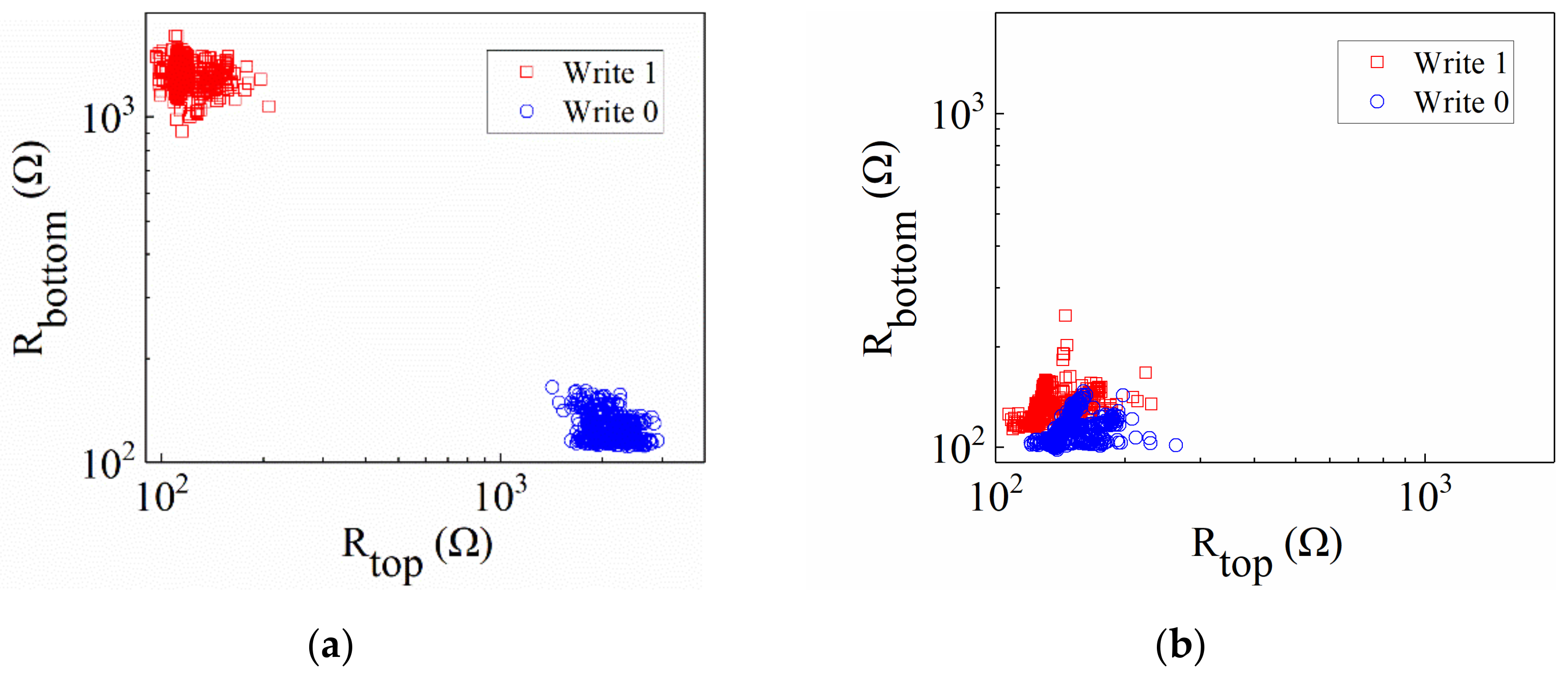
) when ‘1’ was initially written in the cell. However, an intermediate voltage was measured after masking regardless of the initial written value. In fact, the two sets of voltage measurements are overlapped. Thus, it is unlikely to predict whether ‘0’ or ‘1’ is stored under the masked state.
The resistances of the devices derived from the results in
Figure 13 are represented in
Figure 14. After the unmasking operation (
Figure 14a) both devices are in different resistance states, depending on which value was written to the cell in advance. However, once masked, both devices remain in the
. The resistance values are quite similar regardless of the value initially stored in the cell, as observed in
Figure 14b. Therefore, these results demonstrate that we can deterministically determine the switching RRAM of the cell, i.e., writing the desired data to the cell (0 or 1), and we can subsequently mask and unmask the previous written data repeatedly.
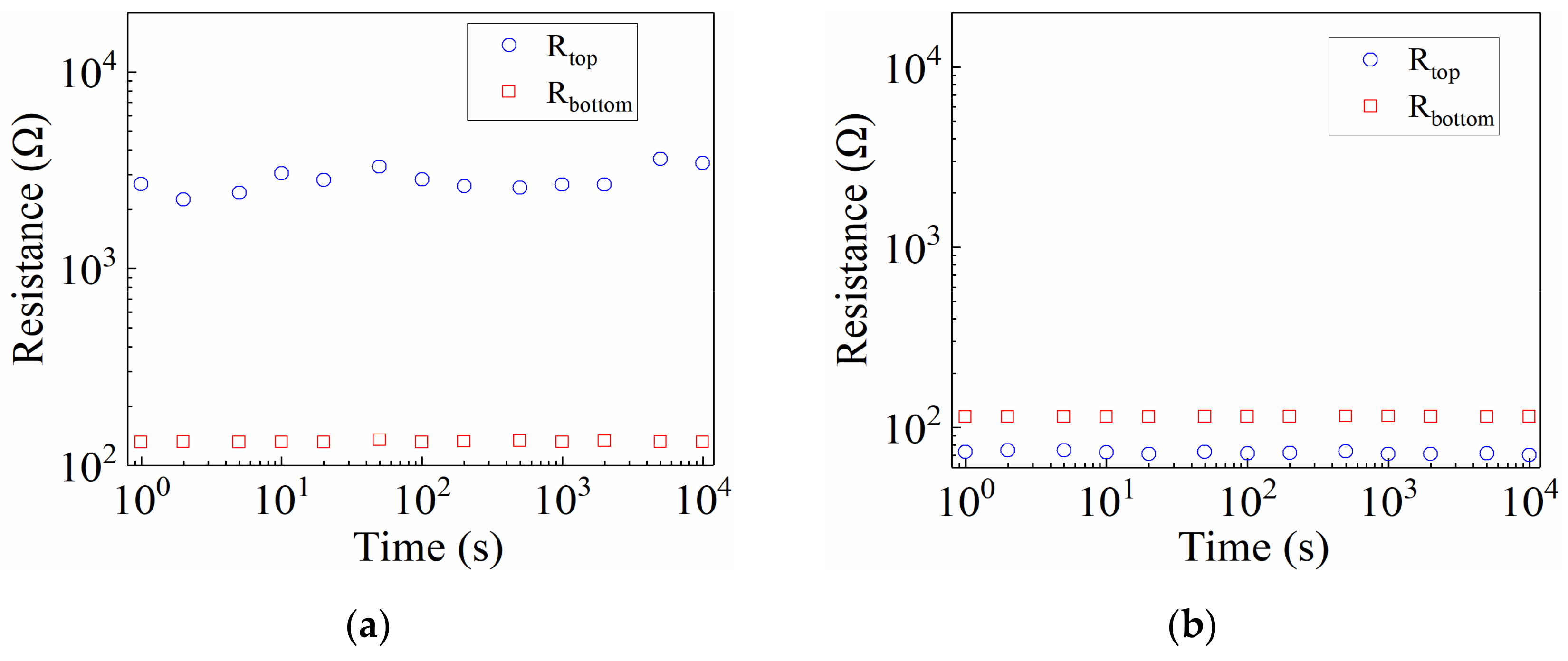
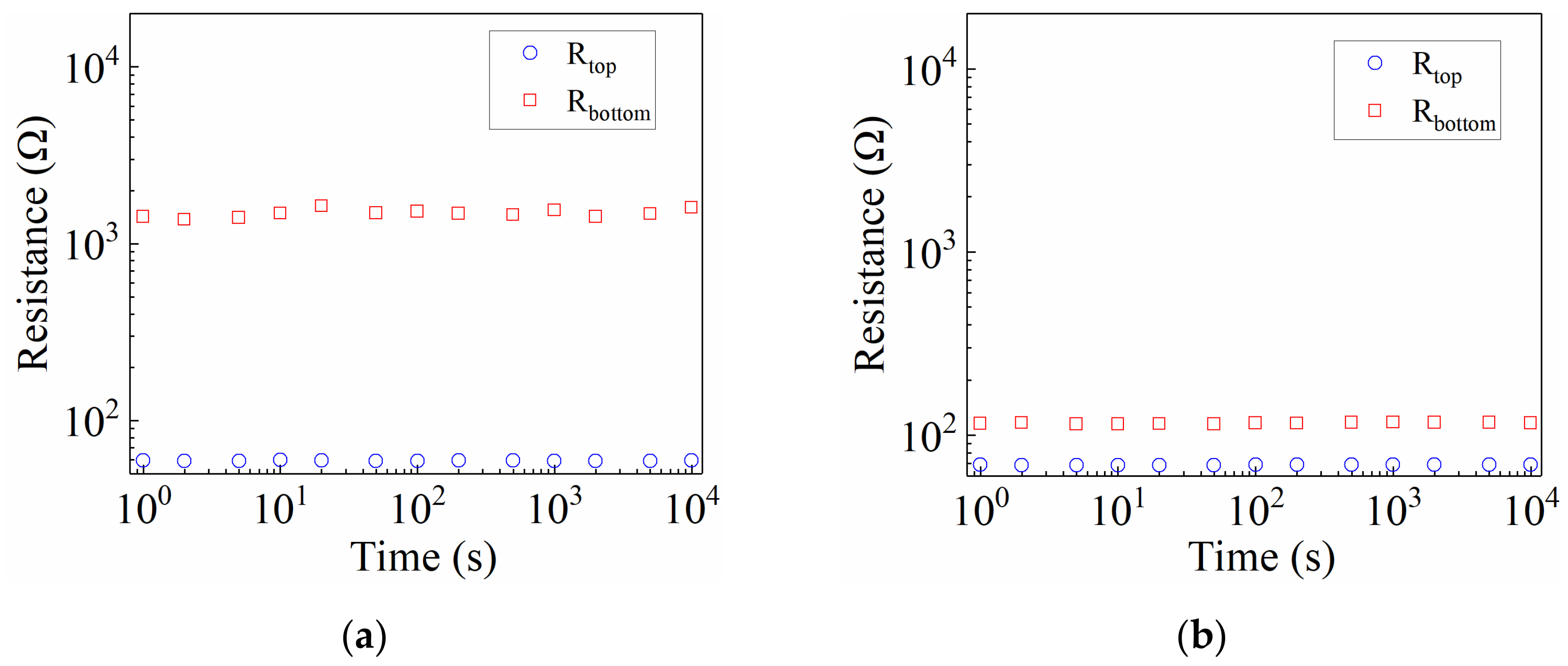
Experiments were also conducted to check the behavior of the masked bit over time. In particular, the goal consisted in extending the masked state for 10
4 s, verifying throughout the experiment that it was stored (masked) successfully. The corresponding results showing the resistance values of the RRAMs are shown in
Figure 15a,b when ‘0’ was initially written to the cell. The equivalent values are presented in
Figure 16a,b when ‘1’ was initially written to the cell. The results confirm that the bit can be unmasked and masked for at least 10
4 s.
The final experiment focused on observing the behavior of the cell in case we want to modify the bit stored in the cell. For this purpose, a sequence of 1000 write-masking-read-unmasking-read operations was applied, where the write operations (write-0 or write-1) were randomly selected. An illustrative example of the behavior of the cell is reported in
Figure 17. The resistances of the two devices are derived from the read operations after unmasking (
Figure 17a) and masking (
Figure 17b). The switching device is always the expected RRAM, according to the value written to the cell. Furthermore, the resistances in the
of the two RRAMs are very similar in the masked state regardless of the previous write operation. In fact, the two sets of points overlap, as observed in
Figure 17b. This feature, which allows rewriting the cell many times, confirm the use of this cell as a memory cell. In fact, it can also be exploited for reconfiguration purposes or the removal of the information stored in the cell in those applications where the information is rarely updated. In fact, these results, together with the capability of masking and unmasking the data, confirm the suitability of this cell for application in secure NVMs.
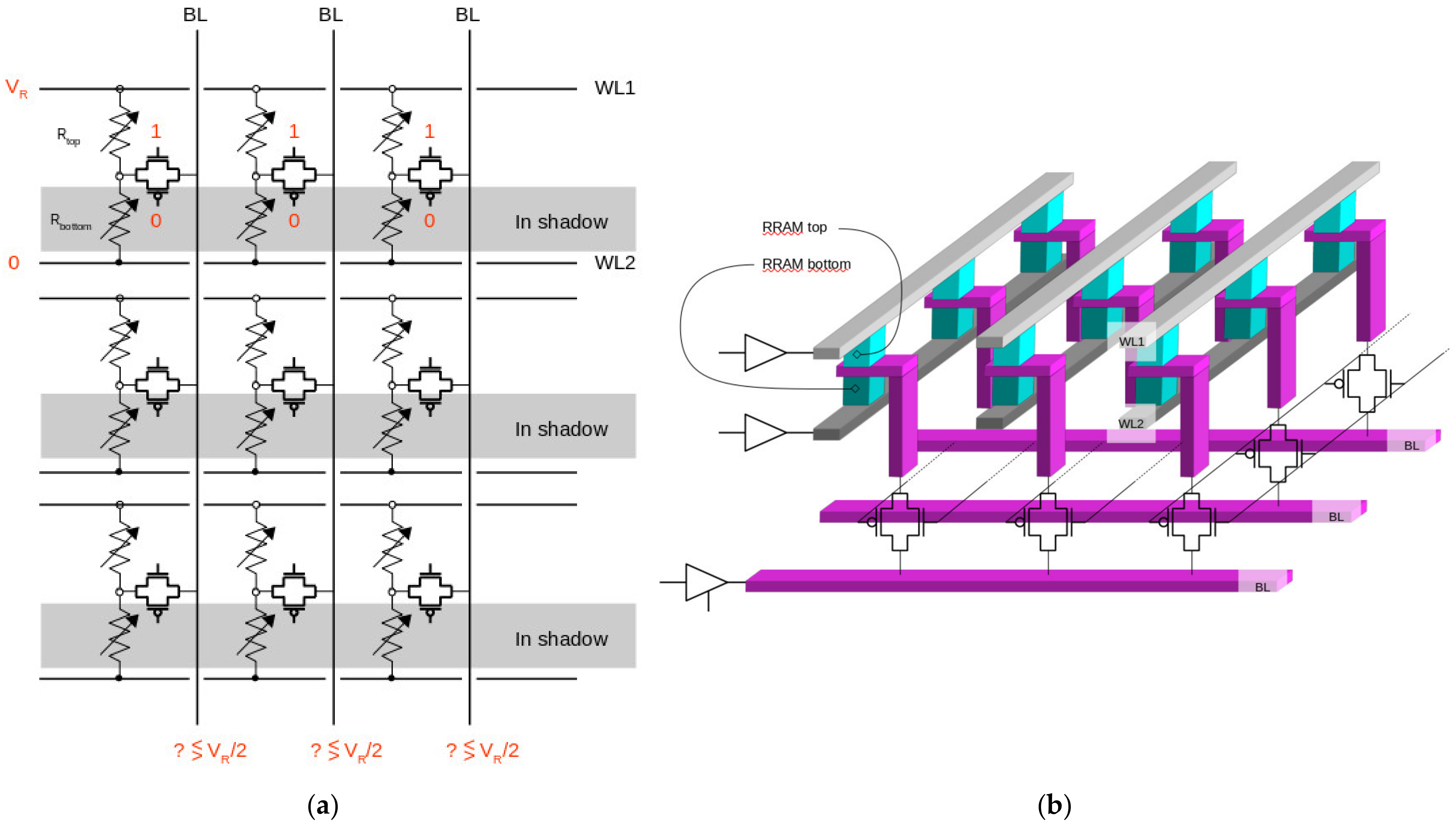
5. Array Architecture
The experimental results presented in the previous section demonstrate that the serial RRAM cell can be exploited to store one bit of information with masking capability. Hence, it is feasible to combine multiple cells into an array structure to derive a secure NVM. A cross-point array could be considered for this purpose. However, some design modifications are required to derive the serial RRAM cell, i.e., connecting the bottom electrode of the top device to the top electrode of the bottom device. This array meets the requirements from the operational point of view, but it also adds security vulnerabilities in the presence of a physical attack. In fact, as all the devices are in the same layer, this configuration exposes node
Vap2 (see
Figure 3) so that an attacker may contact this node without destroying the cell structure, with the potential risk of leak of information. In this context, we propose a multilayer array architecture, as illustrated in
Figure 18. Multilayer RRAMs is a technology that has been already proposed as a way for building denser memories [
44,
45,
46], therefore it can also be leveraged for this serial RRAM cell configuration, avoiding the need of a specific array design or technology, which could discourage its implementation. Two word-lines are necessary to bias nodes
(WL1) and
(WL2) while nodes
are connected through transmission gates to the bit lines. As it is indicated in
Figure 18a, for reading the cells in one word-line, WL2 is grounded and the reading voltage is applied to WL1. Transmission gates are enabled and voltages at BLs are compared for extracting the bit information. Typically, the reading process is made by word lines steps. Initially, the cells in one word line are unmasked, read and masked again before moving to the next word line. In this way, most of the cells remain masked during most of the time. Although every cell is composed of two devices, the proposed architecture provides similar performance in terms of scalability when compared to other RRAM security primitives, which consider differential sensing, requiring thus also two devices to derive a single bit.
Figure 18b shows a 3D illustration of the memory array. Two layers of RRAMs are used. The lower layer contains the bottom RRAMs whereas the upper layer contains the top RRAMs. The lower layer (labeled as the shadow in
Figure 18a) is placed so that their geometric position coincides with the upper layer. This gives them a natural sheet protection against physical attacks as it is discussed next.
6. Security Features
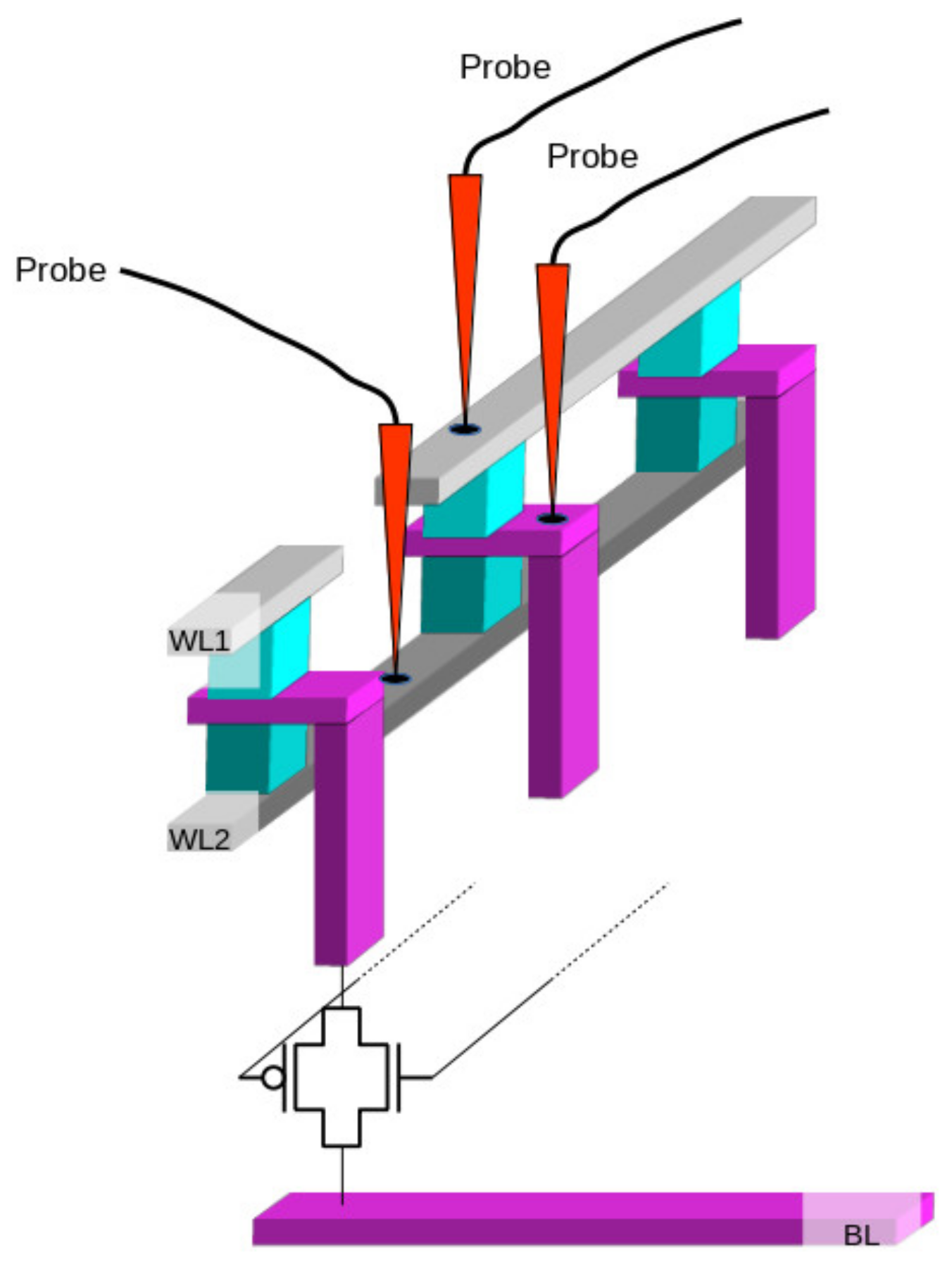
The memory array based on a serial RRAM cell presents advantages against physical and side-channel attacks. In the case of physical attacks, it is plausible to assume that the adversary cannot read the content of on-chip resources nor the data bus since on-chip components are trustworthy (data protection techniques at a higher level are assumed to be active in the system) during its operation. However, off-chip components, such as the memory modules, or on-chip elements while the chip is powered off, are assumed to be vulnerable since the attacker is considered to have physical access using reverse engineering techniques. In this situation, a potential memory array based on serial RRAM cells embraces the same security performance against physical attacks as other RRAM-based memories. Furthermore, as there is no charge stored in RRAMs, the states are not exposed by charge-detection-type attacks, as they may be in floating-gate-based EEPROM/Flash memories. An adversary may try to measure passively RRAM resistances to reveal the state of the cell and therefore the stored bit. However, both RRAMs of the same cell are at the LRS in the masked state. Thus, reading the top device is not enough to get the information. The attacker would need also to measure the bottom one and then apply some types of reasoning trying to envisage the unmasked bit. Accessing the bottom RRAM is not easy and definitively makes the attack considerably complicated. As shown in
Figure 19, using FIB edition a vertical cut must be opened which would break WL1 and thus would corrupt the operation of the memory array. If metallization depositions are made in order to restore the connection, easily they would become into a short circuit between WL1 and WL2 lines. An alternative to the passive measurement of resistances would be to contact the intermediate node
and try to detect the voltage during the read operation. Despite not impossible, it is highly probable that the parasitic effects of the probe, which will be significant at this scale, will alter the unmasking process giving a wrong bit as a result. Even in a context where RRAM devices are reverse-engineering without destroying the storage structure, it would not be possible to differentiate between ‘0’ and ‘1’ by using high-resolution microscopy, since the two devices of every cell are in the LRS (masked state) as the attack is performed when the system is powered off. Therefore, despite not impossible, the difficulty to reach a successful physical attack in the serial RRAM memory array is expected to be much higher than that in the standard memory array.
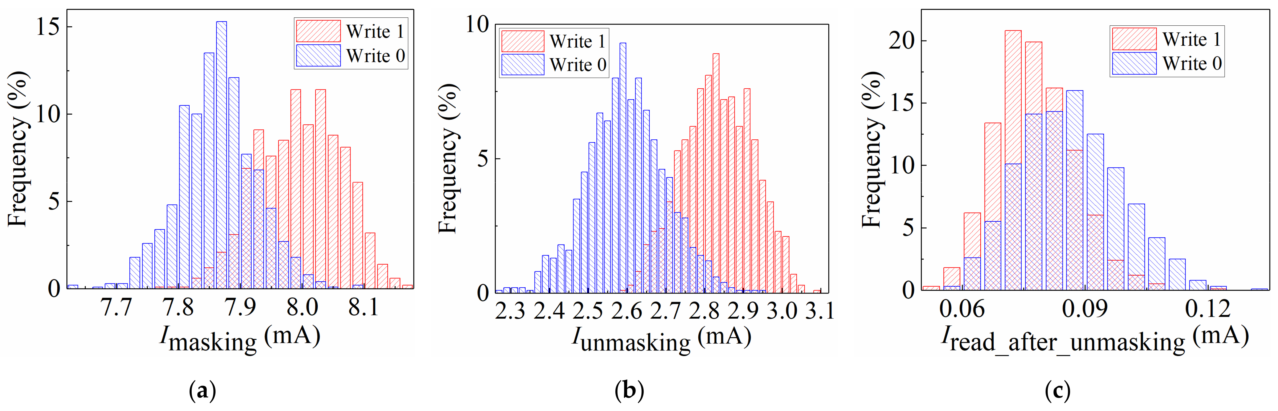
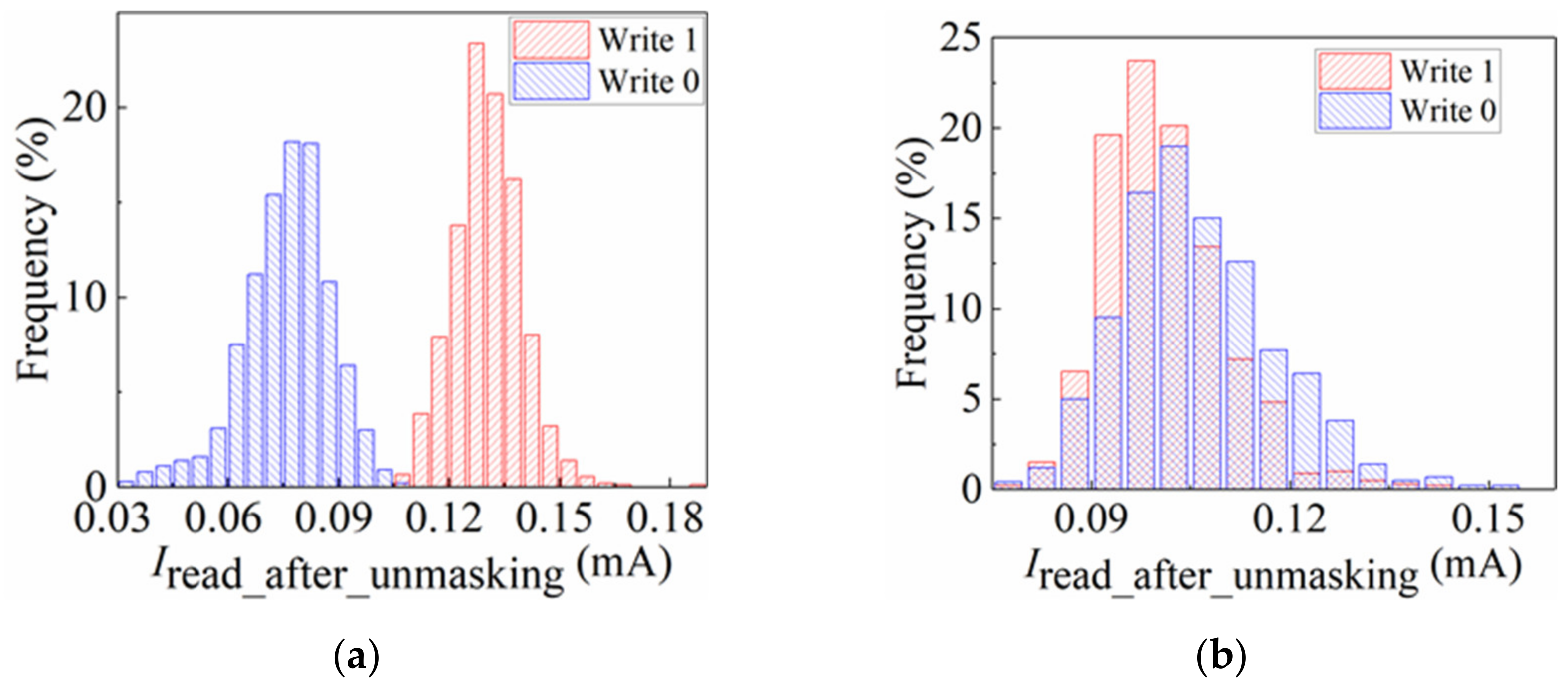
The side-channel attack is one of the most widely adopted methods to steal private data in the hardware security field, which exploits the different signatures in current information when reading/writing ‘1’ and ‘0’ bits. Therefore, one way to protect against the side-channel attack is trying to eliminate the difference in current information when operating with ‘1’ and ‘0’ bits. The proposed serial RRAM cell in this work achieved this point by causing the operation currents to be uncorrelated with the data stored in the cell. In the masking operation, it is always that one of the RRAM devices is in the HRS whereas the other one in the LRS no matter which bit is stored in the cell. In this case, the current information for any masking operation with ‘1’ or ‘0’ bit is relatively similar. The same analysis applies to the unmasking and read operations, in the former of which both RRAM devices of the cell are in the LRS regardless of which bit is stored in the cell whereas the latter faces the same distribution of RRAM resistance states as the masking operation. Hence, the current consumption of a given cell is dependent on the detailed resistance state of RRAM devices, but independent on the stored bit. The inherent cycle-to-cycle and device-to-device variability of RRAMs result in different current consumption behaviors among cells, preventing an unintended leakage of information. To illustrate this fact, the quiescent current consumption of a serial RRAM memory cell during masking, unmasking and read (after unmasking) operation for 1000 cycles is shown in
Figure 20a–c, respectively. Both situations, initially applying a write-1 and a write-0 have been considered. Regardless of the value initially written to the cell, the current consumption is similar in every operation. Although the distributions are not completely overlapped, the extraction of information for a particular cell is not worthy to predict the behavior of the remaining cells, since every cell has its particular behavior depending on the inherent variability and stochasticity of the devices. This fact is shown in
Figure 21, where the quiescent current consumption during a read operation (after unmasking) is presented for two more cells, in a similar way as it has been presented in
Figure 20c.
These memory cells refer to three different serial RRAM memory cells, each of which is composed of two RRAM devices in series. The three representative examples illustrate three different behaviors in terms of current consumption during read after unmasking operation. For cell 1 (
Figure 20c), the current consumption is slightly higher when a ‘0’ has been written to the cell. On the contrary, cell 2 (
Figure 21a) presents higher current consumption when a ‘1’ has been written to the cell and cell 3 (
Figure 21b) presents an almost completely overlapping between the two distributions, becoming more similar to the behavior of cell 1. Therefore, the serial RRAM cell does not present distinguishable current signatures, which may minimize the possibility of information leakage.
The serial cell provides also the feature of rewriting the content, maintaining the masking capability, as it has been previously shown in
Figure 17. This fact paves the way for memory reconfiguration, which can be utilized to update the information or for fresh re-keying [
47,
48]. When the original key has been revealed or the ownership is revoked and the user needs a new key, this scheme is useful, which can also limit the side-channel exposure of per-key. In fact, the same scheme can be also used for shredding when the key is no longer needed. In any case, it must be taken into account that a memory array based on the serial RRAM cell can be combined with other existing security features, at different levels, to improve the security performance of the resulting primitive.


 ,
, 


