
On the VCO/Frequency Divider Interface in Cryogenic CMOS PLL for Quantum Computing Applications


1
Department of Enzo Ferrari Engineering, University of Modena and Reggio Emilia, Via Vivarelli, 10, int. 1, 41125 Modena, Italy
2
CNR-IMM Unit of Agrate Brianza, Via Olivetti, 2, 20864 Agrate Brianza, Italy
*
Author to whom correspondence should be addressed.
Electronics 2021, 10(19), 2404; https://0-doi-org.brum.beds.ac.uk/10.3390/electronics10192404
Submission received: 1 September 2021
/
Revised: 27 September 2021
/
Accepted: 28 September 2021
/
Published: 1 October 2021
(This article belongs to the Collection Analog IC Design—Analog and RF Interface for Electronic Systems)
Abstract
:The availability of quantum microprocessors is mandatory, to efficiently run those quantum algorithms promising a radical leap forward in computation capability. Silicon-based nanostructured qubits appear today as a very interesting approach, because of their higher information density, longer coherence times, fast operation gates, and compatibility with the actual CMOS technology. In particular, thanks to their phase noise properties, the actual CMOS RFIC Phase-Locked Loops (PLL) and Phase-Locked Oscillators (PLO) are interesting circuits to synthesize control signals for spintronic qubits. In a quantum microprocessor, these circuits should operate close to the qubits, that is, at cryogenic temperatures. The lack of commercial cryogenic Design Kits (DK) may make the interface between the Voltage Controlled Oscillator (VCO) and the Frequency Divider (FD) a serious issue. Nevertheless, currently this issue has not been systematically addressed in the literature. The aim of the present paper is to investigate the VCO/FD interface when the temperature drops from room to cryogenic. To this purpose, physical models of electronics passive/active devices and equivalent circuits of VCO and the FD were developed at room and cryogenic temperatures. The modeling activity has led to design guidelines for the VCO/FD interface, useful in the absence of cryogenic DKs.
1. Introduction
Since ancient times, humankind has always been in need of computing; computation capability and knowledge progress have always walked arm in arm. In 1948 the discovery of the transistor triggered a revolution, paving the way for the modern microprocessors, which are at the base of the actual computation-based information society [1,2,3]. The microprocessor, by manipulating a huge amount of bits per second, allowed humans to face and solve problems of amazing difficulty in mathematics, physics, chemistry, and engineering. In the XXI century a new kind of microprocessor appeared, the quantum microprocessor. It manipulates bits but of a very special type: the quantum bit, or qubit. The qubit enjoys the counterintuitive properties of the quantum world, such as superposition and entanglement. For the superposition principle, a qubit can be in a superposition of states. Therefore, contrary to its classical counterpart, a qubit can assume 0 and 1 values at the same time. Generally speaking, the superposition allows for a massive parallelism, as introduced in 1985 by David Deutsch in his landmark paper [4]. Once two qubits interact, they are selectively correlated, becoming a new physical entity, not reducible to the two original single qubits. Two entangled qubits cannot be independently manipulated, even if they are far away. Superposition and entanglement allow for algorithms not possible on a classical microprocessor, promising a radical leap forward in a variety of different scientific, social, and economic contexts, spanning from finance to security and medical sectors. Nevertheless, in order to be efficient, these quantum algorithms should run on a quantum microprocessor where superposition and entanglement are physically available and not emulated, as it may be on a classical microprocessor. This calls for the fabrication of quantum microprocessors. Silicon-based spintronic qubits appear to be a very attractive alternative to the currently widely used transmon technology. From a technological point of view, they are indeed compatible with the actual CMOS microelectronics. In 1998, Kane already proposed the fabrication of quantum microprocessors by using the CMOS technology [5]. From an engineering point of view, the manipulation of silicon-based qubits requires frequencies that can be synthesized using the actual CMOS Radio Frequency Integrated Circuits (RFIC). Phase-Locked Loop (PLL) and Phase-Locked Oscillator (PLO), typically used for the frequency synthesis, offer phase noise properties that may be useful in the qubit control. When embedded in a quantum microprocessor, the RFIC should be operated at cryogenic temperatures. Currently, this poses challenges because usually the foundries do not deliver Design Kits (DK) at cryogenic temperatures. In particular, this issue may be critical for PLL/PLO, because of the frequency matching required between two of its important building blocks: the Voltage Controlled Oscillator (VCO) and the Frequency Divider. Generally speaking, as one can expect, this matching is temperature dependent, as the PLL/PLO may be prevented from correctly working when the temperature falls to cryogenic values. Nevertheless, this issue has not been systematically addressed in the literature. The aim of the present paper is to investigate the frequency mismatch that may arise between the VCO and the Frequency Divider when the temperature drops from room to cryogenic values. The paper is organized as follows. Section 2 introduces the qubit implementation with special regard for the silicon-based solution. Section 3 addresses the issues of an integrated CMOS PLL/PLO when used to synthesize frequencies for the qubit control. Section 4 is devoted to the modeling of transistors and passive components at both room and cryogenic temperature. Section 5 focuses on the design of the two critical building blocks, VCO and Frequency Divider. In particular, the effects of the temperature on the frequency behavior of these circuits are modeled. Considerations on the models lead to some design guidelines, briefly described in Section 6, for VCO and Frequency Divider useful when the cryogenic DK for the chosen technology is not available. Section 7 closes the paper by drawing some conclusions.
2. Qubit and Silicon Microelectronics
Generally speaking, every microscopic two-state quantum physical system can be exploited as a qubit. Currently, superconductor and trapped ions are the technologies at the heart of the first generation of commercially pre-competitive quantum microprocessors. Semiconductor nanostructures, neutral ions, and photons provide a valid alternative to achieve comparable results in the medium term. In particular, silicon technology, despite a delay in terms of maturity with respect to the two more cutting-edge technologies (superconductors and trapped ions), is definitely in strong competition with them for several reasons.
First, under a solid-state physics point of view, the confinement of electron and nuclear spins in host semiconducting materials represents a versatile platform for the realization of qubit. The electron confinement into a quantum dot is achievable following different approaches, from electrostatically and self-assembled quantum dots to donor spins in solid matrices or a combination of them [6]. Several qubit realizations are presented in the literature where the logical states |0> and |1> are encoded in single-electron spin in a quantum dot, singlet-triplet spin states in double quantum dot, three electrons spin states in triple quantum dot, or an all-electrical realization of quantum dot qubit, where three electrons are confined in a double quantum dot, called hybrid qubit [7]. Analogous qubit realizations are achieved for the donor scenario [8].
The fabrication of a complete silicon fault-tolerant architecture is an ambitious task rewarded with the possibility of using the well assessed CMOS technology semiconductor manufacturing. Semiconductor nanostructured qubits offer, therefore, the exciting potentiality of paving the way towards the large-scale quantum computation era based on the same silicon chip technology of the current information age.
Moreover, silicon qubits outperform other competitors in terms of quantum information density, i.e., the number of physical qubits per unit area. For silicon qubits this quantity goes from 830 to 105 Mqubit/cm2, which is significantly larger than superconductors and trapped ions qubits, for which it lies in the 10−4–10−5 Mqubit/cm2 range. In addition, the chip area, i.e., the area covered by 2 billion physical qubits, goes from 10–102 mm2 for semiconducting qubits to 107–1010 mm2 for superconductors and trapped ions qubits [9].
Semiconductor nanostructured qubits are attractive also for their relatively long coherence times, which allows for the execution of a higher number of quantum gate operations. The silicon crystal, once made free from its 29-isotope, is a relatively noise-free environment for spintronic qubits.
Easy manipulation and fast gate operations are other benefits offered by the qubits on silicon. Regarding the qubit manipulation, for single-electron spin qubits in a quantum dot, the microwave frequency useful for its control, that corresponds to the energy difference between the two spin states, is in the 13–40 GHz frequency range. The frequency grows for the single-electron spin qubits in a donor for which lies in the 30–50 GHz range. These control frequency ranges are very attractive, because in the last two decades, the microelectronics industry for telecom applications demonstrated that such kind of signals can be generated and manipulated by using CMOS RFICs. Therefore, again, the CMOS technology seems to be an interesting option for the fabrication of quantum microprocessor.
In short, on the basis of the previous discussion, one can conclude that silicon-based qubits sound very appealing, because of higher versatility, higher information density, longer coherence times, and compatibility with CMOS technology and RFIC microelectronics.
3. PLL/PLO and Quantum Microprocessors
The typical circuit frequency synthesizer used in CMOS RFIC is the PLL/PLO, the typical building block diagram of which is shown in Figure 1. In a PLL, the Frequency Divider in the feedback loop is programmable, while in a PLO it is not. The PLL/PLO constitutes a feedback loop, the goal of which is to control the frequency generated by the VCO. When locked, the PLL/PLO sets the VCO to oscillate at a frequency N times the reference frequency, where N is the division modulus of the Frequency Divider. Overall, the PLL/PLO therefore works as a frequency multiplier. A very interesting property of the PLL/PLO is the shaping effect of the feedback loop on the phase noise when the PLL/PLO is locked. On the right, Figure 1 shows that close to the carrier, the PLL/PLO phase noise is lower with respect to the free running VCO. The integral phase noise therefore decreases when the PLL/PLO instead of the VCO is used for the frequency synthesis. In telecom applications this property is useful because it helps with keeping low the Bit Error Rate (BER) at the receiver side. Interestingly, this property turns out to be useful also for the control of a qubit. The signal controlling the qubit in a quantum microprocessor should exhibit indeed an integral phase noise as low as possible, because a too large integral phase noise may jeopardize the quantum gate fidelity [10], a sort of BER for the qubit. The PLL/PLO therefore appears to be an interesting candidate radiofrequency source for a quantum microprocessor [10,11]. A survey of the recent literature reveals that, under the pressure of packing together a large number of qubits, being the estimated goal for the quantum supremacy in the range of tens of millions, the actual envisage solution is moving the classical CMOS circuitry closer to the qubits by levering on the actual microelectronics technology [12,13,14,15,16,17,18,19,20,21,22,23,24,25,26]. The design of cryogenic CMOS circuitry for a quantum microprocessor is a real multi-faceted activity covering RFIC [12,17,22,24,26], DAC [16,24,26], readout circuits [22,25], and more general aspects related to the microprocessor architecture [15,23,25] and to the cryogenic system, as well. This makes a quantum microprocessor closer to a mixed-signal than a pure digital circuit. The CMOS circuit design depends, moreover, also on the qubit implementation (transmonic, spintronic, single, double, triplet) [13,14].
Therefore, an integrated CMOS PLL appears to be a very interesting electronic cell for the design of the measure-and-control layer of a quantum microprocessor. It is worth noting that classical microprocessors also currently embed several PLLs.
The interface between the VCO and the digital Frequency Divider is a very challenging issue in the design of a PLL/PLO. The Frequency Divider exhibits indeed an optimal frequency fOPT, at which the required level of the input signal is minimum, making easier the design of the VCO. The larger the offset from fOPT is, the higher the amplitude of the VCO signal should be. If the frequency offset is too large, the PLL/PLO cannot achieve the locking condition. In this case, the VCO runs free, and its frequency goes out of control. As in a quantum microprocessor, the integrated CMOS PLL/PLO is placed close to the qubits, and it should operate at cryogenic temperature. In reality, this involves a practical issue for the microelectronics designer: the lack of commercial Design Kits (DK) available at cryogenic temperatures [11]. Currently, the silicon foundries usually release DK in the −50 °C to +80 °C temperature range. The actual praxis is therefore designing the RFICs at room temperature by using a standard process and then cooling down the prototypes to cryogenic temperatures for its characterization [27,28]. As the cooling down from 300 K to a cryogenic temperature may induce a frequency mismatch between the VCO and the Frequency Divider, the RFICs are designed with generous tolerances and tuning capabilities, entailing a sub-optimized design. In the worst cases, these tolerances may not be enough to prevent the PLL to achieve the locking condition. In this frame, the investigation of the critical interface between the VCO and the Frequency Divider when the temperature changes from room to cryogenic is of large interest. Nevertheless, in spite of that, this issue has not been systematically investigated in the literature. The present paper intends to investigate the frequency mismatch between the VCO and the Frequency Divider that may arise when the temperature drops from room to cryogenic values.
4. Cryogenic Models
In the present work, the first step was to address the cryogenic modeling of the devices to be used for the design of the VCO and of the Frequency Divider. A cryogenic temperature of 4 K is assumed, because of the recent demonstrations of silicon-based qubits able to operate at temperatures higher than 1 K instead of the usual sub −1 K range [29,30]. A higher operating temperature allows for a higher cooling power for the dilution fridge. This turns into a greater power dissipation headroom available for the microelectronics engineer. The estimated power budget roughly rises from 1 mW to 1 W, when the operating temperature increases from 100 mK to 4 K.
Several compact models are reported in the literature for MOSFET operating at cryogenic temperature: MOS11, PSP, and BSIM [31,32,33]. In these works, the models were improved by adding additional Verilog-A software modules. The present work adopts the MOS3 compact model due to its simplicity and allowing the modeling of second order effects like the short-channel effect and mobility degradation without additional Verilog-A code. This makes the models compatible with the large set of SPICE-based circuit simulators. In particular, cryogenic MOS3 models were extracted for n-channel and p-channel MOSFET with gate length of 40 nm and gate widths of 1200 nm and 120 nm from the data reported in [32]. During the design, these two different sized MOSFET form a small set of transistors, which can be connected to obtain equivalent transistors of different aspect ratio. It is worth noticing that the modeling procedure takes advantage of the absence of kink effect in the transistor output characteristics, as it is expected for gate length shorter than 0.7 µm [31,32].
One of the most important parameters for the MOS3 model is the threshold voltage, VTO. Its value was extracted from the experimental transcharacteristics reported in [32]. The obtained results are reported in Table 1. Another important model parameter is PHI, which is the threshold surface potential φST. At room temperature is provide by the usual expression:
where VTH is the thermal voltage, ni the intrinsic carrier concentration, and NA the substrate doping concentration. When the temperature goes down to cryogenic, φST changes by ΔφF in the case of an n-channel MOSFET [34]:
where
where α = gAexp[(EA − Ei)kT], with ground-state degeneracy factor, EA the energy level of the acceptor impurity and Ei the intrinsic Fermi energy level. The quantity α accounts for the dopant incomplete ionization; in the case of complete ionization α = 0 and thus ΔφF = 0. The values of PHI computed from these equations are reported in Table 1. Moving from the work of Beckers et al. [34], it is possible to demonstrate that the threshold voltage VTN of an n-channel MOSFET with n-type doped poly-silicon gate is given by:
where NC is the effective state concentration in the conduction band, εSi the silicon dielectric permittivity, and C′ox the gate capacitance per unit area.
By using an oxide thickness of 1.7 nm reported in [32], assuming a dielectric permittivity equal to the silicon dioxide, default for the MOS3 model, and a substrate doping of few 1018 cm−3, typical for deep sub-micron CMOS technologies, the previous equation gives VTN = 0.53 V at room temperature and VTN = 0.61 V at cryogenic temperature, in good agreement with the range of the extracted values for VTO. Because of the field ionization occurring under the Si/SiO2 interface [34,35,36], the NA was kept equal to its room temperature value. The thickness oxide model parameter TOX was set equal to 1.7 nm.
The transconductance coefficient KP parameter, the ETA parameter for the DIBL effect and the THETA parameter for the mobility degradation were first extracted by following basic extraction techniques described in [37,38]. Next, parameters KP, ETA and THETA were used as fitting parameters in order to obtain the same behavior of the measured DC characteristics, together with the source and drain resistance parameters RS and RD, respectively. The values obtained for KP, ETA and THETA are reported in Table 1. The obtained RS and RD values of 10 Ω were kept common for all the transistors. A gate resistance parameter RG of 15 Ω was adopted from [39].
To complete the models, gate resistance and parasitic capacitances have to be added. For the model parameters CBD, CBS, CGSO and CGDO, describing the parasitic capacitances per unit channel width, typical values for a 45 nm technology [38,40,41] were assumed. In particular, for the substrate related capacitances CBD and CBS, it was set CBD = CBS = 0.45 fF/μm (CBD = CBS = 0.6 fF/μm) for an n-channel (p-channel) MOSFET at room temperature. For the overlap capacitances CGSO and CGDO, it was set CGSO = CGDO = 0.5 fF/μm. When the temperature decreases from room to cryogenic values, the drain-substrate and source-substrate parasitic capacitances CBD and CBS drop by a factor of ten, because these parasitic capacitances are associated to the space charge region of a reversed biased on junction [42]. In agreement, the cryogenic values of the model parameter CBD and CBS are ten times smaller than the corresponding room temperature values. On the other hand, the overlap gate-source and gate-drain capacitances CGSO and CGDO are temperature independent.
The flicker noise model parameters used for KF and AF for 40 nm technology were from [43]. The value of AF remains nearly one over the temperature range from room temperature down to cryogenic temperature; the value of KF is temperature independent for n-channel MOSFET [44,45,46]. The values for AF and KF used are also listed in Table 1, where the parameters for the PMOS transistor are also reported.
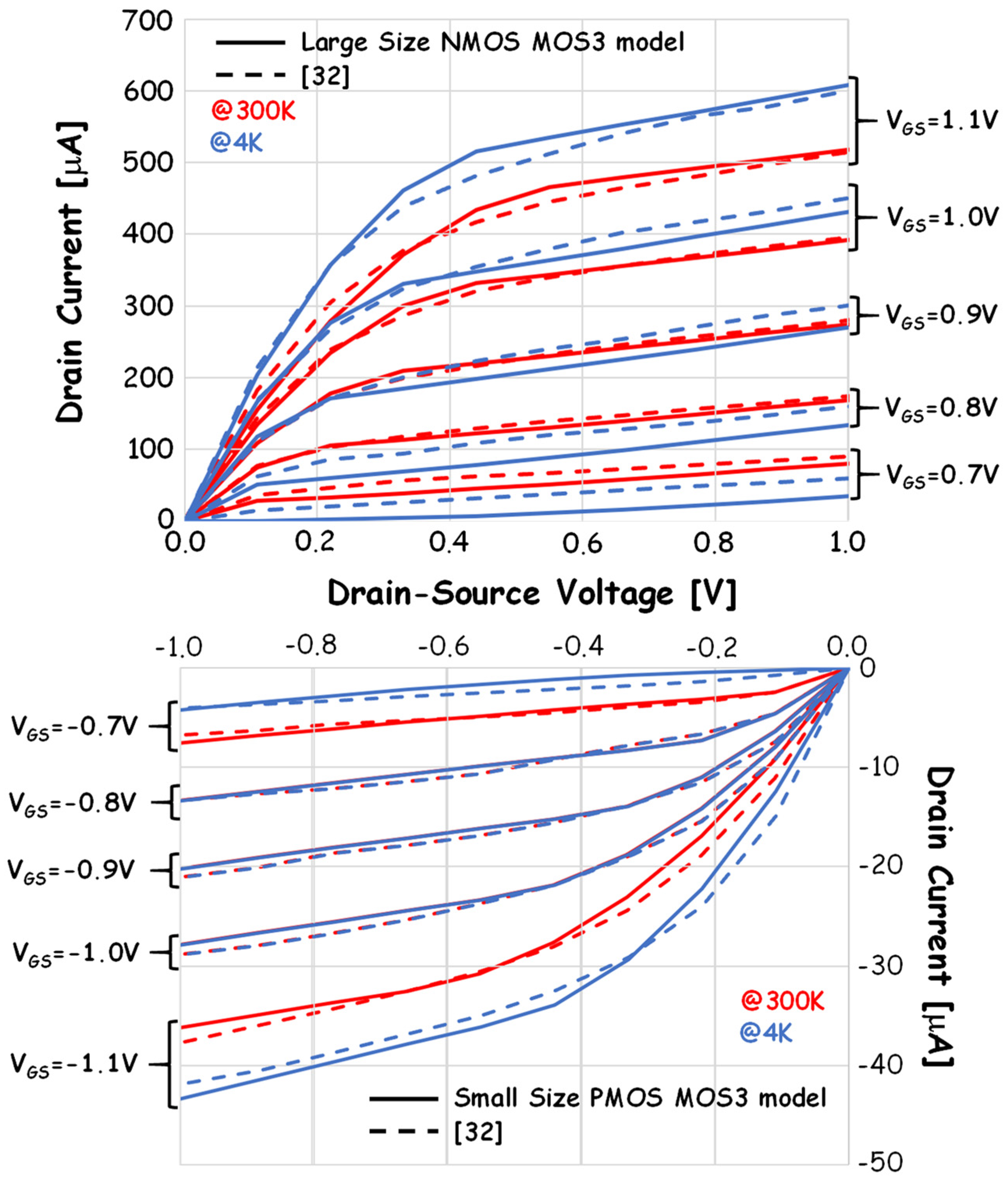
The extracted MOS3 models are able to reproduce the output characteristics reported in [32] pretty well, both at room temperature and at 4 K. In particular, Figure 2 addresses the large-size NMOS and the small-size PMOS. The absolute error between the experimental and the MOS3 drain currents is about 3.2% (9.5%) for the large-size NMOS transistor at 300 K (4 K) and about 5% (14%) for the small-size PMOS transistor at 300 K (4 K). A similar good agreement was also obtained for the other transistors.
Poly-Si resistors and Metal-Oxide-Metal (MOM) capacitors maintain their values at deep-cryogenic temperatures, while the inductor exhibits a reduction of the inductance of approximately 5% and an improvement of the quality factor [47,48]. Therefore, only the inductor needs cryogenic modeling. In the present work, it was assumed a simplified compact model constituted by an inductor in series with a resistor, accounting for the metal losses and skin effect. The substrate losses were modeled by placing a resistor in parallel to the previous RL circuit. As an effect of reducing the temperature down from room to cryogenic, the series resistance drops by about 40%, while the parallel resistance increases by three orders of magnitude.
5. VCO and Frequency Divider
The VCO and Frequency divider were first designed at 300 K and then simulated at 4 K, in order to investigate the effect of the temperature decrease on the critical interface between the VCO and the Frequency divider. Following the considerations carried out in the Introduction, VCO and Frequency divider were designed to operate around 15 GHz.
5.1. Voltage Controlled Oscillator: Design and Modeling
Figure 3 depicts the VCO schematic adopted in the present work. It is a differential oscillator, whose core is the cross-coupled pair of n-channel transistors M1 and M2 providing the energy required to maintain the oscillation. The inductors and the capacitors C are the resonator, which fix the oscillation frequency fOSC. The capacitor C is designed by using MOM capacitors or similar, because their capacitance does not change with the temperature [48]. This frequency is tunable, because of the varactors, implemented by using capacitor connected p-channel MOSFETs. The tuning voltage Vtune is applied on the gate of these transistors. The resistors Rp and Rs in the inductor model account for the losses in the inductors, as previously described.
They set the quality factor Q of the inductor at a given frequency f0:
Figure 3, on the right side, depicts the equivalent small-signal model of the differential admittance YDiff. In this model the two cross-coupled transistors M1 and M2 are equivalent to the differential negative resistance RNEG = −2/gm1(2), where gm1(2) is the transconductance of the transistors M1 and M2, whose parasitic capacitances are accounted for by the two capacitors Cp. As shown in the figure, the inductors, but not the fixed capacitors and the varactors, participate to define YDiff. When the fixed capacitors and the varactors are also accounted for, one gets the linearized model of the VCO. In this way, YDiff can be exploited as the core of the oscillator, whose oscillation frequency can be later tuned by adding the fixed capacitors C and the varactors. The linear model on the right side in Figure 3 returns the following mathematical expression:
where s is the Laplace complex variable. By putting s = jω = j2πf and after some algebraic manipulations, one gets the dependence of YDiff on the frequency:
Oscillations can start up if YDiff exhibits a negative real part, that is:
Under these conditions, YDiff injects into the resonator more energy than that dissipated by Rp and Rs. Of course, the higher the injected energy, the higher the oscillation of the differential output signal vout = v+out − v−out. In particular, for a given vout, the value of the bias current IBIAS can be estimated from the inductor model by describing the transistor during the oscillator operation as an ideal switch [49]:
On the other hand, the imaginary part of YDiff can be described, due to the series of two inductors whose inductance Leq is expressed by the following mathematical expression:
The capacitance of the fixed capacitor C should resonate, at the free running frequency f0 of the VCO, with these two equivalent inductors. The values for C can be therefore estimated through the usual formula of the LC resonance frequency:
With these equations in mind, the VCO was designed at room temperature by using the scattering parameters. As depicted in the previous Figure 3, the circuit, without the fixed capacitor and the varactors, was excited by a couple of ports, with the same characteristic impedance Z0, at the frequency of interest f0. The circuit is therefore described as a two port network through the four scattering parameters S11, S12, S21, and S22. The differential reflection coefficient ΓDiff can be obtained from these parameters through the following formula:
from which YDiff can be obtained as:
The inductors used in the present design were set equal to 0.75 nH. Assuming a quality factor of 10 and a f0 = 15 GHz, Equation (1) gives Rp = 1413 Ω and Rs = 3.53 Ω. By choosing a peak-to-peak differential output voltage of 1 V, IBIAS results to be about 560 μA from Equation (9). The start-up condition, see Equation (8), implies gm1(2) > 1.4 mS. By choosing gm1(2) = 3.2 mS, the transistor overdrive is about 0.18 V; the aspect ratio of the transistors M1 and M2 results to be about 3.6/0.04. In order to keep the gate length in the range of 1 μm, each transistor was obtained as the parallel of three transistors with an aspect ratio of 1.2/0.04. The supply voltage VDD was set equal to 1V, in order to keep the dissipated power low.
With these values, the scattering parameter simulation gave YDiff = −(880 + j6440) μS at 15 GHz. The simulated value of the real part of YDiff is close to the value of −893 μS, provided by Equation (7). The small difference has to be ascribed to the channel modulation effect. The transistor output characteristics in Figure 2 show its presence but, for the sake of simplicity, it was not accounted for in the equivalent small-signal model in Figure 3. The simulated value of the imaginary part of YDiff results are very close to the value of 6470 μS predicted by Equation (7), by putting the transistor parasitic capacitance Cp = 12.5 fF. At 15 GHz, the imaginary part of YDiff corresponds to Leq = 0.82 nH, from which Equation (11) gives C = 68.6 fF.
Figure 4 reports, on the left side, the waveforms of the differential carrier vout generated by the oscillator working at 300 K. The start-up phase, during which the small-signal approximation applies, last about 4 nsec. Afterward, the transistor non-linearities make the oscillator enter the steady state regime, where the oscillation frequency is 15 GHz and the peak-to-peak amplitude is close to 1V. In order to get the desired frequency, the value of C was tuned to 69 fF. This tuning is a consequence of the non-linearities excited in the steady state regime.
Once the correct behavior of the oscillator at room temperature was observed, the oscillator was simulated at 4 K by using the cryogenic models for transistors and inductors. Concerning the inductors, following what was stated in the previous section, Rp increased by three orders of magnitude, Rs reduced by about 40%, and L decreased by about 5%. The transistors model was modified in agreement with Table 1. As the tail bias current IBIAS was kept constant, the cryogenic transconductance resulted to be about 3.9 mS and the transistor overdrive weakly decreased to 0.14V. The obtained waveforms are depicted on the right side of Figure 4. The duration of the start-up phase reduced to about 1 nsec and the steady state oscillation differential amplitude increased to about 3.2 V, in agreement with the reduction of the losses in the inductor. The cryogenic values of the inductor model parameters give indeed a quality factor of about three times higher than that at 300 K. A more ideal reactive response of the inductor allows therefore to get oscillation amplitudes higher than the supply voltage. It is worth noticing that Equation (9) predicts a differential output amplitude vout = 3.15 V when the increased value of Rp and the decreased value of Rs at cryogenic temperature are used.
The oscillation frequency increases to about 15.4 GHz, compatible with the 5% reduction in the inductance. The increased quality factor of the inductor leads also to an improvement in the phase noise as depicted in Figure 5. The phase noise spectrum at room temperature exhibits a slope of −20 dB/dec, indicating that is dominated by up-conversion of thermal white noise. When the temperature falls to 4 K, the phase noise magnitude decreases and the slope changes to about −30 dB/dec, a signature that the phase noise at cryogenic temperature is dominated by up-conversion of the flicker noise; at this temperature the white noise up-conversion appears for frequency offset higher than 100 MHz. The phase noise simulations in Figure 5 were carried out by using the Harmonic Balance method. They account for the up-conversion of the low frequency noise only and not for the phase noise floor. It is worth citing here that, for an oscillation frequency of about 13 GHz, quite close the 15 GHz addressed in the present work, a phase noise floor of −145 dBc/Hz was reported for a 40 nm CMOS VCO working at 3.5 K [28].
The VCO tuning capability was obtained by adding PMOS varactors, as sketched in Figure 3. Figure 6 shows on the left side the capacitance-voltage characteristics of the used varactor. The two characteristics are shifted by about 0.1 V, in agreement with the variation observed in the threshold voltage of the PMOS transistors. With the same procedure used for the NMOS transistors, from the data reported in [32], it was indeed found that the threshold voltage of the PMOS transistors decreases of about 150mV when the temperature drops from room to cryogenics values.
The previous Equation (7) can be modified into YDiff,OSC, in order to also take into account the fixed capacitances C and the varactors capacitance CVAR as well:
At the oscillation frequency ωOSC, the inductor resonate out with the capacitor and imaginary part of YDiff,OSC (jω) should be zero:
Some algebraic manipulations give the following mathematical expression of ωOSC:
Figure 6 compares, on the right side, the tuning voltage characteristics of the VCO obtained from the non-linear transient simulations (bold curve) with that predicted by the linear small-signal model (open circles) depicted on the right in Figure 3, but this time by accounting for the fixed capacitors and the varactors, as well, and by neglecting the excitation ports #1 and #2, previously used to simulate YDiff. The value of C was reduced by about 32 fF with respect to the value of 69 fF, in order to account for introduction of the varactors (2C + CVAR = 2 × 69 fF). The obtained curves show a fairly good agreement; a small difference has to be expected, because of the transistor non-linearities excited during the simulations in the time domain. In particular, the differences are more pronounced at cryogenic temperatures, because the oscillation amplitudes are larger. The application of the model shows that the vertical shift in the two characteristics is due to the 5% variation in the inductance induced by the temperature.
5.2. Frequency Divider: Design and Modeling
The front-end electronics of a Frequency Divider usually takes the form of a fixed modulus or of a dual-modulus Frequency Divider. As depicted in Figure 7, in the present work, it was a divide-by-two Frequency Divider obtained by closing in a negative feedback a register, constituted by a cascade of two static Current Mode Logic (CML) latches in a master-slave configuration driven by counter-phase clocks.
Because bias voltage VDD is 1V, in order to save bias headroom, the clock differential pair MC was biased by applying a voltage VBias on their gate, as in [50,51], instead of using the traditional tail current solution, that requires to stack further transistors. The CML is coupled to the VCO with the coupling capacitor CBias. The RBias resistors avoid that the AC component of the clock coming from the VCO is drained to ground. RBias and CBias work therefore as a bias tee. The latch is constituted by two differential pairs. The driver differential pair MD works like a differential amplifier; it is activated when the clock is high. The latch is in the transparent phase, because it samples the input differential signals D and Dbar. When the clock goes down, the circuit enters the opaque phase. In this phase the latching differential pair ML is active, and it stores the signal previously sampled by the MD pairs. When only the DC component of the clock is applied, because of the negative feedback used for the register, the Frequency Divider behaves like a CML ring oscillator [50,52] exhibiting a self-oscillation frequency fSO. The condition for the self-oscillation is captured by the following equation [52]:
where WD and WL are the channel width of the driving and latching transistors, respectively. During the self-oscillation the oscillation amplitudes are usually large enough to excite the non-linearities. The transconductances of the transistors in the circuit are therefore time variant. In Equation (17) gm,L is the DC value of the time variant transconductance of the ML transistors [52] and CPAR is the parasitic capacitance, highlighted in red in the schematic, at each drain terminal of the MD transistors. The previous Equation (17) for the self-oscillation implies:
Equation (18) means that the cross-coupled ML transistors should generate a small-signal equivalent negative resistance able to compensate the losses due to the load resistors RD. It is also worth presenting the mathematical expression of fSO reported in [53] in the case of a Frequency Divider constituted by n latches, where n is even.
where |ILSO| and |IDSO| are the modules of the phasors, rotating at 2πfSO pulsation, of the currents flowing in the MD and ML transistors, respectively, under the self-oscillation condition. For n = 2, as in the present case, the previous equation reduces to the following one:
This equation is similar to Equation (19), and it suggests that |IDSO|/WD should be equal to |ILSO|/WL.
When the clock is applied, the Frequency Divider can be described as an injection locked oscillator. The amplitude of the input clock signal useful to lock the oscillator exhibits its minimum when the clock input frequency fCLK is 2fSO [50,54]. In the case of a frequency offset Δf between 2fSO and fCLK, the minimum clock amplitude VCLK,min, needed to keep the Frequency Divider correctly working, increases; the larger Δf, the higher VCLK,min. The plot of VCLK,min versus fCLK, called the Frequency Divider sensitivity curve, exhibits therefore a typical V-shape centered around 2fSO [54]. For excessively large Δf, the Frequency Divider enters the cut-off region. The V-shaped sensitivity curve can be reproduced through the following formula [50]:
where Kinj is an injection parameter describing how much the current injected by the clock signal is stronger than the DC current.
In the present work, RD was kept equal to 1070 Ω, requiring a gm,L higher than 935 μS, corresponding to a minimum bias current of about 20 μA for the ML transistors. This condition was satisfied, both at 300 K and 4 K, by choosing WD and WL equal to 4800 nm, leading to a bias current of about 139 μA and 120 μA at 300 K and 4 K, respectively, for both the MD and ML transistors.
Figure 8 compares self-oscillation waveforms and the sensitivity curves for the Frequency Divider simulated at 300 K and 4 K. The self-oscillation frequency shifts from 13.6 GHz to 15.6 GHz when the temperature drops from 300 K to 4 K.
Since fSO is inversely proportional to the time constant RCPAR, (see Equations (19)–(21)), to investigate the fSO shift induced by the temperature change it is useful to get a rough estimation of this time constant. Following [53] the parasitic capacitance CPAR was estimated as sum of several contributes. Focusing on the node in Figure 8, one can write:
In this expression, CDB,D1 and CGD,D1 are the drain-bulk and the overlap gate-drain capacitances, respectively, of the MD1 transistor, CGD,L1 and CGS,L1 are the overlap gate-drain and gate-source capacitances of the ML1 transistor, CGD,L2 is the overlap gate-drain capacitance for the ML2 transistor, COX,L1 is the gate oxide capacitance of the ML1 transistor and CLOAD is the capacitive load provided by the input node of the following register. In Equation (23), the CGD,L1 and CGD,L2 capacitances are multiplied by two, because they are excited by a differential signal. Since the input node is constituted by the gate of the MD2 transistor of the following register, the CLOAD capacitance can also decomposed in several contributes:
where CGD,D2 and CGS,D2 are the overlap gate-drain and gate-source capacitances of the MD2 transistor and COX,D2 is the gate oxide capacitance of the MD2 transistor. Because the MD and ML transistors have been sized at minimum length and with the same channel width, it is reasonable to consider all the overlap parasitic capacitances equal to a given value COV, CDB,D1 and CDB,L2 equal to a given value CDB, and COX,L1 and COX,D2 equal to a given value COX,LD. By replacing Equation (24) into Equation (23) one gets:
In Equation (25) only the capacitance COV can be considered constant during the self-oscillation and independent of temperature. On the other hand, the capacitance CDB depends on time, because it depends on the voltage present at the drain of the transistor, and it depends also on the temperature [42] while the capacitance COX,LD depends only on the time. For a given temperature, Equation (25) contains therefore two time-dependent capacitive contributes, whose average values have to be estimated. The estimation was carried out by assuming that the transistors behave like a switch during the self-oscillation with a given duty cycle δ.
When the transistor is on, since it is biased in the saturation region, COX,LD,ON can be estimated to be 2/3εOX/tOX. The drain current ID flowing in the channel causes now a voltage drop on the load resistor R and therefore the CDB exhibits its high value, CDB,ON, because the reverse voltage across the drain-bulk junction is -VDD+IDRD. Finally, the resistance RDS of the channel can be estimated as VDS/ID. In this case, the resistance at the drain node RON, with the transistor on, can be estimated as reported in [52]:
When the transistor is off the COX,LD,OFF capacitance was assumed to be 10% of COX,LD,ON, because it is constituted only by the substrate space charge region capacitance, being that the channel is absent. The drain voltage can be assumed equal to VDD, because there is no voltage drop on the load resistor, zero being the drain current of the transistor. Therefore, the CDB exhibits its low value, CDB,OFF, because the reverse voltage across the drain-bulk junction is -VDD. In addition, the resistance of the channel can be assumed infinite, because the drain current of the transistor is zero. The resistance at the drain node RD,OFF, with the transistor off, is therefore simply equal to RD.
On the basis of the previous considerations, the average value of the COX,LD capacitance can be therefore estimated as:
and the average value of the CDB capacitance as:
Similarly, the average value of the resistance at the drain node can be estimated as:
In this way the self-oscillation frequency can be estimated by replacing average values of CPAR and R into Equation (19):
where WD/WL was taken equal to one, because the MD and ML transistors are sized with the same channel width.
With the parameter values reported in Table 1, the used device size, the simulated drain currents, and a duty cycle of 40%, it is possible to compute <R> = 870 Ω, <CPAR> = 23.5 fF at 300 K and <R> = 873 Ω, <CPAR> = 20.9 fF at 4 K, leading to 2fSO = 14.9 GHz at 300 K and 2fSO = 16.9 GHz at 4 K. The comparison with the values of 2fSO obtained from the simulation (see Figure 8) gives an error of about 10% at 300 K and of about 8% at 4 K. On the other hand, the 2fSO shift predicted by Equation (30) results to be the same as obtained from simulations. This agreement suggests that the increase of the self-oscillation frequency is mainly due to the drop of one order of magnitude of the drain-substrate and source-substrate parasitic capacitances CBD and CBS [42]. The average value of the resistance at the drain node changes very little.
Figure 8 also compares the simulated sensitivity curves obtained from transient simulations with the sensitivity curves predicted by Equation (22). A general fairly good agreement was achieved by setting Kinj = 1450mV for the sensitivity curve at 300 K and Kinj = 800mV for the curve at 4 K. In both the cases, it is possible to remark that the agreement is better for frequency higher than 2fSO. A similar asymmetrical agreement between the upper side and the lower side of the sensitivity curve was observed also for the more complex model proposed in [52]. It is worth noticing that the injection factor decreases by about 50% as a consequence of the temperature drop, leading to wider sensitivity curve, as it is possible to observe this in the figure. For a given frequency offset from 2fSO, the Frequency Divider needs a lower amplitude of the clock signal at cryogenic temperature. At cryogenic temperature, the Frequency Divider seems therefore working better.
6. Design Guidelines
The modeling activity developed in Section 3 for the temperature effect on the frequency behavior of the VCO and of the Frequency Divider suggest some guidelines in the absence of an available Design Kit at cryogenic temperatures for the adopted technology. Concerning the VCO, the carried-out considerations suggest that the VCO can be designed using the available 300 K Design Kit but considering a 5% reduction in the inductance of the tank inductor [47,48] and a variation in the transistor threshold voltage, which can be estimated by using the cryogenic modeling described in Section 2. Similarly, even the Frequency Divider can be designed by using the 300 K available Design Kit, but by taking into account that the bulk-drain capacitances at 4 K are one order of magnitude lower than at 300 K [41]. Usually, the designer can find information about process parameters useful for these evaluations in the Design Rule Manual (DRM) or, at least, by investigating the technical literature.
It is worth noticing here that the investigation of the Process-Voltage-Temperature corners, the Montecarlo analysis, and the Post-Layout-Simulations are necessary steps for the robust design of oscillators [55,56,57] and Frequency Dividers [58,59]. Nevertheless, in the absence of cryogenic DKs, these investigations can be carried out only at room temperature. The proposed guideline may therefore be considered also as a useful integration to make up for the absence of the statistical data needful for the corner and Montecarlo analysis at cryogenic temperature, also in light of the first experimental evidence on the mismatch in MOS technology at cryogenic temperature reported in [31].
7. Conclusions
The PLL appears attractive for the generation of the microwave signals to control the qubits, because of its interesting phase noise properties. VCO and Frequency Divider interface is very critical for a correct operation of the PLL, because an excessive frequency mismatch between VCO and frequency may prevent the PLL to reach the lock condition. The unavailability of a cryogenic Design Kit is currently a quite common situation, as VCO and Frequency Divider are designed at room temperature, without insights on the frequency mismatch between the VCO and the Frequency Divider may rise up at cryogenic temperatures. The present work addressed by means of simulations the effects of the temperature drop, from 300 K down to 4 K, on the frequency behavior of a differential LC VCO and a static CML Frequency Divider designed in a 40 nm CMOS technology.
After having presented cryogenic models of both active and passive components, VCO and Frequency Divider were simulated and their frequency behavior were investigated. In particular, for the VCO a linear model was adopted while for the Frequency Divider a time-variant model was preferred. The modeling suggests that the frequency variations observed in the VCO, as a consequence of the temperature drop, have been mainly ascribed to changes in the threshold voltage of the transistors and in the inductance of the tank inductor. Concerning the Frequency Divider, the modeling suggests that the variations in the self-oscillation frequency, induced by the temperature drop, are mainly due to the reduction of the bulk-drain parasitic capacitances.
In the absence of an available Design Kit at cryogenic temperatures, the previous conclusions may be a rough useful guideline for the microelectronics designer. They suggest indeed that the VCO can be designed using the available 300 K Design Kit but considering a 5% reduction in the inductance of the tank inductor [47,48] and a variation in the transistor threshold voltage, which can be estimated by using the cryogenic modeling described in Section 3. Even the Frequency Divider can be designed by using the 300 K available Design Kit but by taking into account that the bulk-drain capacitances at 4 K are one order of magnitude lower than at 300 K [42].
Author Contributions
Conceptualization, G.G., E.F. and M.B.; Methodology, G.G. and M.B.; Software, G.G.; Validation, G.G., E.F. and M.B.; Formal analysis, M.B.; Investigation, G.G., E.F. and M.B.; Data curation, G.G., E.F. and M.B.; Writing—original draft preparation, G.G., E.F. and M.B.; Writing—review and editing, G.G., E.F. and M.B.;Visualization, G.G., E.F. and M.B.; Supervision, M.B.; All authors have read and agreed to the published version of the manuscript.
Funding
This research received no external funding.
Data Availability Statement
All the data are reported/cited in the paper.
Conflicts of Interest
The authors declare no conflict of interest.
References
- Lojek, B. History of Semiconductor Engineering; Springer: Berlin/Heidelberg, Germany, 2007; ISBN 978-3-642-07064-8. [Google Scholar] [CrossRef]
- Riordan, M.; Hoddeson, L. Crystal Fire: The Birth of the Information Age; Norton & Co.: New York, NY, USA, 1997; ISBN 0-393-04124-7. [Google Scholar]
- McCartney, S. ENIAC: Triumphs and Tragedies of the World’s First Computer; Berkley Publishing Group, Penguin Group: New York, NY, USA, 1999; ISBN 978-0802713483. [Google Scholar]
- Deutsch, D. Quantum theory, the Church-Turing principle and the universal quantum computer. Proc. R. Soc. Lond. 1985, 400, 97–117. [Google Scholar] [CrossRef]
- Kane, B. A silicon-based nuclear spin quantum computer. Nature 1998, 393, 133–137. [Google Scholar] [CrossRef]
- Zwanenburg, F.A.; Dzurak, A.S.; Morello, A.; Simmons, M.Y.; Hollenberg, L.C.L.; Klimeck, G.; Rogge, S.; Coppersmith, S.N.; Eriksson, M.A. Silicon quantum electronics. Rev. Mod. Phys. 2013, 85, 961–1019. [Google Scholar] [CrossRef]
- Russ, M.; Burkard, G. Three-electron spin qubits. J. Phys. Condens. Matter 2017, 29, 1–35. [Google Scholar] [CrossRef] [Green Version]
- Morello, A.; Pla, J.J.; Bertet, P.; Jamieson, D.N. Donor Spins in Silicon for Quantum Technologies. Adv. Quantum Technol. 2020, 3, 1–17. [Google Scholar] [CrossRef]
- Ferraro, E.; Prati, E. Is all-electrical silicon quantum computing feasible in the long term? Phys. Lett. A 2020, 384, 1–8. [Google Scholar] [CrossRef] [Green Version]
- Patra, B.; Incadela, R.M.; van Dijk, J.P.G.; Homulle, H.A.R.; Song, L.; Shahmohammadi, M.; Bodgan Staszewski, R.; Vladimirescu, A.; Babaie, M.; Sebastiano, F.; et al. Cryo-CMOS Circuits and Systems for Quantum Computing Applications. IEEE J. Solid-State Circuits 2018, 53, 309–321. [Google Scholar] [CrossRef] [Green Version]
- Manthena, V.; Miryala, S.; Deptuch, G.; Carini, G. A 1.2-V 6-GHz Dual-Path Charge-Pump PLL Frequency Synthesizer for Quantum Control and Readout in CMOS 65-nm Process. In Proceedings of the IEEE Annual Ubiquitous Computing, Electronics & Mobile Communication Conference (UEMCON), New York, NY, USA, 28–31 October 2020. [Google Scholar]
- Charbon, E.; Sebastiano, F.; Babaie, M.; Vladimirescu, A.; Shahmohammadi, M.; Bodgan Staszewski, R.; Homulle, H.A.R.; Patra, B.; van Dijk, J.P.G.; Incadela, R.M.; et al. Cryo-CMOS Circuits and Systems for Scalable Quantum Computing. In Proceedings of the IEEE International Solid State Circuits Conference, San Francisco, CA, USA, 5–9 February 2017; pp. 264–266. [Google Scholar] [CrossRef]
- Van Dijk, J.P.G.; Charbon, E.; Sebastiano, F. The electronic interface for quantum processors. Microprocess. Microsyst. 2019, 66, 90–101. [Google Scholar] [CrossRef] [Green Version]
- Watson, T.; Philips, S.; Kawakami, E.; Ward, D.; Scarlino, P.; Veldhorst, M.; Savage, D.; Lagally, M.; Friesen, M.; Coppersmith, S. A programmable two-qubit quantum processor in silicon. Nature 2018, 555, 633–636. [Google Scholar] [CrossRef] [Green Version]
- Veldhorst, M.; Eenink, H.G.J.; Yang, C.H.; Dzurak, A.S. Silicon CMOS architecture for a spin-based quantum computer. Nat. Commun. 2017, 8, 1766. [Google Scholar] [CrossRef]
- Nielinger, D.; Christ, V.; Degenhardt, C.; Geck, L.; Grewing, C.; Kruth, A.; Liebau, D.; Muralidharan, P.; Schubert, P.; Vliex, P.; et al. SQUBIC1: An integrated control chip for semiconductor qubits. In Proceedings of the International Workshop on Silicon Quantum Electronics, Sidney, Australia, 13 November 2018. [Google Scholar]
- Bardin, J.C.; Jeffrey, E.; Lucero, E.; Huang, T.; Naaman, O.; Barends, R.; White, T.; Giustina, M.; Sank, D.; Roushan, P.; et al. A 28nm Bulk-CMOS 4-to-8GHz <2mW Cryogenic Pulse Modulator for Scalable Quantum Computing. In Proceedings of the IEEE International Solid State Circuits Conference, San Francisco, CA, USA, 17–21 February 2019; pp. 456–458. [Google Scholar] [CrossRef] [Green Version]
- Charbon, E. Cryo-CMOS: 60 Years of Technological Advances towards Emerging Quantum Technologies. In Proceedings of the Keynote at IEEE 45th European Solid-State Circuit Conference and 49th European Solid-State Device Research Conference, Krakow, Poland, 23–26 September 2019. [Google Scholar]
- Bardin, J. CMOS Integrated Circuits for Control of Transmon Qubits. In Proceedings of the Tutorial at IEEE 45th European Solid-State Circuit Conference, Krakow, Poland, 23–26 September 2019. [Google Scholar]
- Voiginescu, S. Towards monolithic quantum computing processors in production FD-SOI CMOS technology. In Proceedings of the Tutorial at IEEE 45th European Solid-State Circuit Conference and 49th European Solid-State Device Research Conference, Krakow, Poland, 23–26 September 2019. [Google Scholar]
- Sebastiano, F. Cryogenic CMOS interfaces for large-scale quantum computers: From system and device models to circuits. In Proceedings of the Tutorial at at IEEE 45th European Solid-State Circuit Conference and 49th European Solid-State Device Research Conference, Krakow, Poland, 23–26 September 2019. [Google Scholar]
- Mehrpoo, M.; Patra, B.; Gong, J.; Hart, P.A.; van Dijk, J.P.G.; Homulle, H.; Kiene, G.; Vladimirescu, A.; Sebastiano, F.; Charbon, E. Benefits and Challenges of Designing Cryogenic CMOS RF Circuits for Quantum Computers. In Proceedings of the IEEE International Symposium on Circuits and Systems, Sapporo, Japan, 26–29 May 2019; pp. 1–4. [Google Scholar] [CrossRef]
- Meunier, T.; Hutin, L.; Betrand, B.; Thonnart, T.; Pillonet, G.; Billiot, G.; Jacquinot, H.; Cassé, M.; Barraud, S.; Kim, Y.J.; et al. Towards scalable quantum computing based on silicon spin. In Proceedings of the IEEE Symposium on VLSI Technology, Kyoto, Japan, 9–14 June 2019. [Google Scholar] [CrossRef]
- Degenhardt, C.; Artanov, A.; Geck, L.; Grewing, V.; Kruth, A.; Nielinger, D.; Vliex, P.; Zambanini, A.; van Waasen, S. Systems Engineering of Cryogenic CMOS Electronics for Scalable Quantum Computers. In Proceedings of the IEEE International Symposium on Circuits and Systems, Sapporo, Japan, 26–29 May 2019; pp. 1–5. [Google Scholar] [CrossRef]
- Lehmann, T. Cryogenic Support Circuits and Systems for Silicon Quantum Computers. In Proceedings of the IEEE International Symposium on Circuits and Systems, Sapporo, Japan, 26–29 May 2019; pp. 1–5. [Google Scholar] [CrossRef]
- Jazaeri, F.; Beckers, A.; Tjalli, A.; Sallese, J.M. A Review on Quantum Computing: From Qubits to Front-end Electronics and Cryogenic MOSFET Physics. In Proceedings of the IEEE International Conference on Mixed Design of Integrated Circuits and Systems, Rzeszow, Poland, 27–29 June 2019; pp. 15–25. [Google Scholar] [CrossRef]
- Van Dijk, J.P.G.; Patra, B.; Subramanina, S.; Xue, X.; Samkharadze, N.; Corna, A.; Jeon, C.; Sheikh, F.; Juarez-Hernandez, E.; Perez Esparza, B.; et al. A Scalale Cryo-CMOS Controller Wideband Frequency-Multiplexed Control of Spin Qubits and Transmons. IEEE J. Solid-State Circuits 2020, 55, 2930–2946. [Google Scholar] [CrossRef]
- Ruffino, A.; Peng, Y.; Yang, T.Y.; Michniewicz, J.; Gonzalez-Zalba, M.F.; Charbon, E. A Fully-Integrated 40-nm 5-6.5GHz Cryo-CMOS System-on-Chip with I/Q Receiver and Frequency Synthesizer for Scalable Multiplexed Readout of Quantum Dots. In Proceedings of the IEEE International Solid-State Circuit Conference, San Francisco, CA, USA, 13–22 February 2021; pp. 210–212. [Google Scholar] [CrossRef]
- Yang, C.H.; Leon, R.C.C.; Hwang, J.C.C.; Saraiva, A.; Tanttu, T.; Huang, W.; Camirand Lemyre, J.; Chan, K.W.; Tan, K.Y.; Hudson, F.E.; et al. Operation of silicon quantum processor unit cell above one Kelvin. Nature 2020, 580, 350–354. [Google Scholar] [CrossRef] [Green Version]
- Petit, L.; Eenink, H.G.J.; Russ, M.; Lawrie, W.I.L.; Hendrickx, N.W.; Philips, S.G.J.; Clarke, J.S.; Vandersypen, L.M.K.; Veldhorst, M. Universal quantum logic in hot silicon Qubits. Nature 2020, 580, 355–359. [Google Scholar] [CrossRef] [PubMed] [Green Version]
- Hart, P.A.T.; Babaie, M.; Charbon, E.; Vladimirescu, A.; Sebastiano, F. Characterization and Modeling of Mismatch in Cryo-CMOS. IEEE J. Electron Devices Soc. 2020, 8, 263–273. [Google Scholar] [CrossRef]
- Lin, S. Cryogenic Characterization and Modeling of Nanometer CMOS Transistors for Quantum Computing Applications. Thesis in Master of Science in Electrical Engineering. Master’s Thesis, Delft University of Technology, Delft, The Netherlands, 30 September 2016. [Google Scholar]
- Akturk, A.; Eng, K.; Hamlet, J.; Ptbhare, S.; Longoria, E.; Young, R.; Peckerar, M.; Gurrieri, T.; Carroll, M.S.; Goldsman, N. Compact Modeling of 0.35um SOI CMOS Technology Node for 4K DC Operating using Verilog-A. Microelectron. Eng. 2010, 87, 2518–2524. [Google Scholar] [CrossRef]
- Beckers, A.; Jazaeri, F.; Enz, C. Cryogenic MOSFET Threshold Voltage Model. In Proceedings of the 49th European Solid-State Device Research Conference (ESSDERC), Krakow, Poland, 23–26 September 2019; pp. 94–97. [Google Scholar] [CrossRef]
- Beckers, A.; Jazaeri, F.; Enz, C. Characterization and Modeling of 28-nm Bulk CMOS Technology Down to 4.2 K. IEEE J. Electron Devices Soc. 2018, 6, 1007–1018. [Google Scholar] [CrossRef]
- Beckers, A.; Jazaeri, F.; Enz, C. Cryogenic MOS Transistor Model. IEEE Trans. Electron Devices 2018, 65, 3617–3625. [Google Scholar] [CrossRef]
- Arora, A. MOSFET Models for VLSI Circuit Simulation: Theory and Practice; Springer: Wien, Austria; New York, NY, USA, 1993; ISBN 978-3-7091-9249-8. [Google Scholar] [CrossRef]
- Carusone, T.C.; Johns, D.A.; Martin, K.W. Analog Integrated Circuit Design; John Wiley & Sons: Singapore, 2013; ISBN 978-0470770108. [Google Scholar]
- Kan, M.; Man-Kang, I.; Shin, H. Extraction and modeling of gate electrode resistance in RF MOSFETs. In Proceedings of the International Conference on Integrated Circuit Design and Technology, Austin, TX, USA, 9–11 May 2005; pp. 207–210. [Google Scholar] [CrossRef]
- PTM Website. Available online: http://ptm.asu.edu/modelcard/LP/45nm_LP.pm (accessed on 23 October 2020).
- Long Channel Models from CMOS Circuit Design, Layout, and Simulation. Available online: https://cmosedu.com/cmos1/cmosedu_models.txt (accessed on 23 October 2020).
- Dierickx, B.; Warmerdam, L.; Simoen, E.R.; Vermeiren, J.; Claeys, C. Model hysteresis and kink behavior of MOS transistors operating at 4.2 K. IEEE Trans. Electron Devices 1988, 35, 1120–1125. [Google Scholar] [CrossRef]
- Razavi, B. Design of CMOS Phase-Locked Loops: From Circuit Level to Architecture Level; Cambridge University Press: Cambridge, UK, 2020; ISBN 978110862620. [Google Scholar] [CrossRef]
- Chang, J.; Viswanathan, C.R. Low frequency noise in CMOSTs at cryogenic temperatures. In Proceedings of the Workshop on Low Temperature Semiconductor Electronics, Burlington, VT, USA, 7–8 August 1989; pp. 133–136. [Google Scholar] [CrossRef]
- Chang, J.; Abidi, A.A.; Viswanathan, C.R. Flicker noise in CMOS transistors from subthreshold to strong inversion at various temperatures. IEEE Trans. Electron Devices 1994, 41, 1965–1971. [Google Scholar] [CrossRef]
- Binkley, D.; Hopper, C.E.; Blalock, B.J.; Mojarradi, M.M.; Cressler, J.D.; Yong, L.K. Noise performance of 0.35-μm SOI CMOS devices and micropower preamplifier from 77–400 K. In Proceedings of the IEEE Aerospace Conference Proceedings, Big Sky, MT, USA, 6–13 March 2004; pp. 2495–2506. [Google Scholar] [CrossRef]
- Gong, M.J.; Alakusu, U.; Bonen, S.; Dadash, M.S.; Lucci, L.; Jia, H.; Gutierrez, L.E.; Chen, W.T.; Daughton, D.R.; Adam, G.C.; et al. Design Considerations for Spin Readout Amplifiers in Monolithically Integrated Semiconductor Quantum Processors. In Proceedings of the IEEE Radio Frequency Integrated Circuits Symposium, Boston, MA, USA, 2–4 June 2019; pp. 111–114. [Google Scholar] [CrossRef]
- Patra, B.; Mehrpoo, M.; Runo, A.; Sebastiano, F.; Charbon, E.; Babaie, M. Characterization and Analysis of On-Chip Microwave Passive Components at Cryogenic Temperatures. IEEE J. Electron Devices Soc. 2020, 8, 448–456. [Google Scholar] [CrossRef]
- Razavi, B. RF Microelectronics, 2nd ed.; Pearson Education: London, UK, 2021; ISBN 978-0-13-713473-1. [Google Scholar]
- Tang, S.D.; Lin, Y.S.; Huang, W.H.; Lu, C.L.; Wang, Y.H. A Current-Mode-Logic-Based Frequency Divider with Ultra-Wideband and Octet Phases. Prog. Electromagn. Res. M 2019, 68, 89–98. [Google Scholar] [CrossRef] [Green Version]
- Hietanen, M.; Aikio, J.; Akbar, R.; Rahkonen, T.; Paerssinen, A. A 28 GHz Static CML Frequency Divider with Back-Gate Tuning on 22-nm CMOS FD-SOI Technology. In Proceedings of the IEEE Proc 19th Topical Meeting on Silicon Monolitic Integrated Circuit in RF Systems, Orlando, FL, USA, 20–23 January 2019; pp. 1–3. [Google Scholar] [CrossRef] [Green Version]
- Luo, J.; Zhang, L.; Wang, Y.; Yu, Z. Behavioral Analysis and Optimization of CMOS CML Dividers for Millimeter-Wave Applications. IEEE Trans. Circuits Syst.—II Express Briefs 2015, 62, 256–260. [Google Scholar] [CrossRef]
- Zhu, M.; Zhao, D. Geometric Analysis and Systematic Design of Millimeter-Wave Low-Power Frequency Dividers in 65 nm CMOS. IEEE Access 2020, 8, 20658–20665. [Google Scholar] [CrossRef]
- Singh, U.; Green, M. Dynamics of High-Frequency CMOS Dividers. In Proceedings of the IEEE International Symposium on Circuits and Systems, Phoenix-Scottsdale, AZ, USA, 26–29 May 2002; pp. 421–424. [Google Scholar] [CrossRef]
- Behagi, A.; Ghanevati, M. Fundamentals of RF and Microwave Circuit Design: Practical Analysis and Design Tools; Chapter 8; Reformed Free Publishing Association: Jenison, MI, USA, 2020; ISBN 9780692948200. [Google Scholar]
- Castaneda-Avina, P.R.; Tlelo-Cuautle, E.; de la Fraga, L.G. Single-Objective Optimization of a CMOS VCO Considering PVT and Monte Carlo Simulations. Math. Comput. Appl. 2020, 25, 76. [Google Scholar] [CrossRef]
- Dani, L.M.; Mishra, N.; Banchhor, S.K.; Miryala, S.; Doneria, A.; Anand, B. Design and Characterization of Bulk Driven MOS Varactor based VCO at Near Threshold Regime. In Proceedings of the IEEE Subthreshold Microelectronics Technology Unified Conference, Burlingame, CA, USA, 15–18 October 2018. [Google Scholar] [CrossRef]
- Maiti, M.; Chakrabartty, S.; Al-Shidaifat, A.; Song, H.; Bhattacharyya, B.K.; Majumder, A. A 90 nm PVT Tolerant Current Mode Frequency Divider with Wide Locking Range. In Proceedings of the IEEE Nordic Circuits and Systems Conference, Oslo, Norway, 27–28 October 2020. [Google Scholar] [CrossRef]
- Deepak, N.; Seshchalam, D.; Raghavendra, K. A 12 GHz Programmable Frequency Divider. Int. J. Electr. Electron. Comput. Sci. Eng. Special Issue. 2016, pp. 199–203. Available online: https://ijeecse.webs.com/91.pdf (accessed on 23 October 2020).
Figure 1.
Typical building block diagram of a PLL (on the left) and phase noise shaping under locked conditions (on the right).
Figure 1.
Typical building block diagram of a PLL (on the left) and phase noise shaping under locked conditions (on the right).

Figure 2.
Output characteristics of the large-size NMOS (upper) and the small-size PMOS (lower) transistors. Dashed lines: from [32], solid lines from MOS3 model. Red curves: 300 K, blue curves: 4 K.
Figure 2.
Output characteristics of the large-size NMOS (upper) and the small-size PMOS (lower) transistors. Dashed lines: from [32], solid lines from MOS3 model. Red curves: 300 K, blue curves: 4 K.

Figure 3.
N-type cross-coupled oscillator: schematic (left) and small-signal model of the differential admittance YDiff (right).
Figure 3.
N-type cross-coupled oscillator: schematic (left) and small-signal model of the differential admittance YDiff (right).

Figure 4.
Carrier waveforms at 300 K (left) and at 4 K (right).

Figure 5.
Phase noise at 300 K and 4 K.

Figure 6.
Tuning characteristics of the varactor (on the left) and of the VCO (on the right).

Figure 7.
Divide-by-two Frequency Divider.

Figure 8.
Self-oscillation differential output waveforms (on the left) and sensitivity curves (on the right) of the Frequency Divider.
Figure 8.
Self-oscillation differential output waveforms (on the left) and sensitivity curves (on the right) of the Frequency Divider.


Table 1.
Parameters of the MOS3 models for NMOS and PMOS transistors at 4 K and 300 K.
| NMOS Large Size | PMOS Large Size | NMOS Small Size | PMOS Small Size | ||||||
|---|---|---|---|---|---|---|---|---|---|
| Parameter | Unit | Temperature [K] | Temperature [K] | Temperature [K] | Temperature [K] | ||||
| 300 | 4 | 300 | 4 | 300 | 4 | 300 | 4 | ||
| PHI | [V] | 0.9579 | 1.156 | 0.9579 | 1.156 | 0.9579 | 1.156 | 0.9579 | 1.156 |
| VTO | [V] | 0.55 | 0.65 | −0.55 | −0.71 | 0.5 | 0.6 | −0.5 | −0.63 |
| KP | [µA/V2] | 200 | 300 | 81 | 131 | 200 | 300 | 81 | 131 |
| ETA | [–] | 0.16 × 10⁻³ | 0.23 × 10⁻³ | 0.21 × 10⁻³ | 0.23 × 10⁻³ | ||||
| THETA | [V−1] | 1.923 | 1.64 | 1.45 | 0.98 | ||||
| CBD | [F] | 5.4 × 10⁻¹⁶ | 5.4 × 10⁻¹⁷ | 6 × 10⁻¹⁶ | 6 × 10⁻¹⁷ | 5.4 × 10⁻¹⁷ | 5.4 × 10⁻¹⁸ | 6 × 10⁻¹⁷ | 6 × 10⁻¹⁸ |
| CBS | [F] | 5.4 × 10⁻¹⁶ | 5.4 × 10⁻¹⁷ | 6 × 10⁻¹⁶ | 6 × 10⁻¹⁷ | 5.4 × 10⁻¹⁷ | 5.4 × 10⁻¹⁸ | 6 × 10⁻¹⁷ | 6 × 10⁻¹⁸ |
| CGSO | [F/m] | 5 × 10⁻¹⁰ | 5 × 10⁻¹⁰ | 5 × 10⁻¹¹ | 5 × 10⁻¹¹ | ||||
| CGDO | [F/m] | 5 × 10⁻¹⁰ | 5 × 10⁻¹⁰ | 5 × 10⁻¹¹ | 5 × 10⁻¹¹ | ||||
| KF | [FV2] | 3 × 10⁻²⁴ | 5.5 × 10⁻²⁴ | 5.5 × 10⁻²³ | 3 × 10⁻²⁴ | 5.5 × 10⁻²⁴ | 5.5 × 10⁻²³ | ||
Publisher’s Note: MDPI stays neutral with regard to jurisdictional claims in published maps and institutional affiliations. |
© 2021 by the authors. Licensee MDPI, Basel, Switzerland. This article is an open access article distributed under the terms and conditions of the Creative Commons Attribution (CC BY) license (https://creativecommons.org/licenses/by/4.0/).
Share and Cite
MDPI and ACS Style
Gira, G.; Ferraro, E.; Borgarino, M. On the VCO/Frequency Divider Interface in Cryogenic CMOS PLL for Quantum Computing Applications. Electronics 2021, 10, 2404. https://0-doi-org.brum.beds.ac.uk/10.3390/electronics10192404
AMA Style
Gira G, Ferraro E, Borgarino M. On the VCO/Frequency Divider Interface in Cryogenic CMOS PLL for Quantum Computing Applications. Electronics. 2021; 10(19):2404. https://0-doi-org.brum.beds.ac.uk/10.3390/electronics10192404
Chicago/Turabian StyleGira, Gabriele, Elena Ferraro, and Mattia Borgarino. 2021. "On the VCO/Frequency Divider Interface in Cryogenic CMOS PLL for Quantum Computing Applications" Electronics 10, no. 19: 2404. https://0-doi-org.brum.beds.ac.uk/10.3390/electronics10192404
Note that from the first issue of 2016, this journal uses article numbers instead of page numbers. See further details here.