
Inverse Design of a Microstrip Meander Line Slow Wave Structure with XGBoost and Neural Network


Research Center for Electronic Device and System Reliability, Southeast University, Nanjing 210096, China
*
Author to whom correspondence should be addressed.
Electronics 2021, 10(19), 2430; https://0-doi-org.brum.beds.ac.uk/10.3390/electronics10192430
Submission received: 17 August 2021
/
Revised: 24 September 2021
/
Accepted: 5 October 2021
/
Published: 7 October 2021
(This article belongs to the Special Issue High-Frequency Vacuum Electron Devices)
Abstract
:We present a new machine learning (ML) deep learning (DL) synthesis algorithm for the design of a microstrip meander line (MML) slow wave structure (SWS). Exact numerical simulation data are used in the training of our network as a form of supervised learning. The learning results show that the training mean squared error is as low as 5.23 × 10⁻² when using 900 sets of data. When the desired performance is reached, workable geometry parameters can be obtained by this algorithm. A D-band MML SWS with 20 GHz bandwidth at 160 GHz center frequency is then designed using the auto-design neural network (ADNN). A cold test shows that its phase velocity varies by 0.005 c, and the transmission rate of a 50-period SWS is greater than −5 dB with the reflectivity below −15 dB when the frequency is from 150 to 170 GHz. Particle-in-cell (PIC) simulation also illustrates that a maximum power of 3.2 W is reached at 160 GHz with 34.66 dB gain and output power greater than 1 W from 152 to 168 GHz.
1. Introduction
High-frequency millimeter-wave communication is receiving increasing attention due to the development of 6G and next-generation communication networks [1]. It is difficult to realize high-power millimeter-wave sources over the W-band because of the power limitation of solid-state devices [2]. As a core component of high-power microwave devices, the traveling wave tube (TWT) has a wide range of applications in millimeter-wave fields, and has been applied in terahertz wave transmission systems [3]. Compared with solid-state devices, TWTs have obvious advantages at high frequencies [4]. Therefore, it is necessary to carry out research on high-frequency TWT technology to promote the development of high-frequency millimeter-wave technology [5]. Among various types of TWTs, spiral and folded waveguides are the most common slow wave structure (SWS) in the microwave and millimeter-wave bands [6]. In [7], a double corrugated waveguide (DCW) SWS was designed to support a beam voltage of 13 kV with a wide bandwidth of about 20 GHz, obtaining an interaction impedance of approximately 1.5 Ω at D band. An SWS for a W-band folded-waveguide TWT with an operating bandwidth of around 3 GHz was also designed, delivering an output power of 50 W at the operating voltage of 13.5 kV and operating beam current of 80 mA. Obviously, these SWSs require high voltages to provide a high output power, which is the obstacle preventing the application of vacuum electronic device (VED) in modern communication systems.
Planar microstrip meander line (MML) SWSs are more conducive to microfabrication techniques, which can offer simple construction, wide bandwidth and low operation voltage [8]. MML SWSs have demonstrated a low voltage of 3–5 kV at V-band and W-band [9,10]. Recently, Zhen et al. used a concentric arc MML SWS to obtain 44 W output power with 18.6 dB gain working at 720 V [11].
Meanwhile, deep learning (DL) [12,13], a supervised method of pattern analysis with a multilayered structure, has been widely applied in inverse-design over the past decade [14,15]. In current research of inverse-design based on DL, deep neural networks (DNN) are trained using tensors encoded with structure and spectrum characteristics [16,17], demonstrating the use of DL technology as an inverse-design tool in microwave and optical wave fields. In [18], a purpose-designed DL architecture made up of a convolutional neural network (CNN) and a fully-connected neural network (FCNN) was used to automatically model and optimize three-dimensional chiral metamaterials, achieving high numerical accuracy in plasmonic meta-surfaces. The method realized the design-on-demand function and produced suitable meta-atom geometric parameters to fulfill the given requirements. A typical multi-layer FCNN was also successfully applied to solve effective refractive indices of the fundamental waveguide mode in a silicon nitride channel waveguide for both polarizations of light [19]. The DL model was only trained with sixteen data points and could accurately predict patterns in the effective refractive indices. Malkiel et al. introduced a DL architecture that was applied to the design and characterization of metal-dielectric sub-wavelength nanoparticles. Their approach of training a bidirectional network that goes from the optical response spectrum to the nanoparticle geometry and back was significantly more effective than the alternative method of training separate models for design and characterization tasks [20]. This data-driven technique has been applied to tackle challenging problems in a wide range of fields. Applying DL to achieve practical parameters for an SWS is a highly effective method for their design.
While these DL algorithms have very powerful learning and prediction capabilities, their interpretability remains a significant challenge. Especially in the field of VED, where the dimensions of device structure and spectrum are low and the data set is limited, the algorithm could provide sufficient design guidance rather than simply be used as a blackbox function.
This paper aims to rapidly design an MML SWS according to the target center frequency and bandwidth using our proposed algorithm. An XGBoost-DNN composite structure [21] is applied to inverse design a practical MML SWS. The optimized parameters of an MML SWS are then obtained using supervised machine learning algorithms according to the desired bandwidth and center frequency of the MML SWS. The mean squared error (MSE) is reduced to 0.001 using 900 groups of data. An MML SWS is then designed for particle-in –cell (PIC) simulations using the parameters obtained by this method, and the results show that the obtained parameters work well for the MML SWS.
2. MML Structure and Cold Parameters
The unit structure of the proposed MML with a metal shield consists of two parts, the dielectric substrate, and the MML, which are shown in Figure 1. The dielectric substrate material is silicon dioxide (SiO2), the thickness of the dielectric substrate is set as h, the relative dielectric constant ε is 3.75, and the tangent loss, tanδ, is 0.0004. The MML is pure copper, with electrical conductivity at 2e7 S/m. Its thickness is t = 0.01 mm, with a line width of w, a distance between two adjacent transverse microstrip lines of s, and a transverse length of l. H is the height between the MML and metal shield and is fixed at 0.75 mm; L is the transverse width of the metal shield, where L = 2 * ls + l and ls is fixed at 0.2 mm.
The main characterizations of the MML are phase velocity and transmission, which determine the performance of an MML SWS. Therefore, the phase velocity and transmission versus frequency are simulated using CST studio suite. In order to describe the spectrum characteristics of the MML, the characteristic parameters v, d, Smin and Smax from the spectrum shown in Figure 2a,b are defined, where v is normalized phase velocity at the central frequency, d is the difference between the phase velocity at the lower bandwidth and that at the upper bandwidth, which represents the flatness of phase velocity within the required bandwidth.
Figure 2b shows the transmission characteristics of the MML, where the minimum transmission (Smin) and the maximum reflection (Smax) in the bandwidth are defined. These two parameters represent the transmission performance of the MML structure.
3. Method
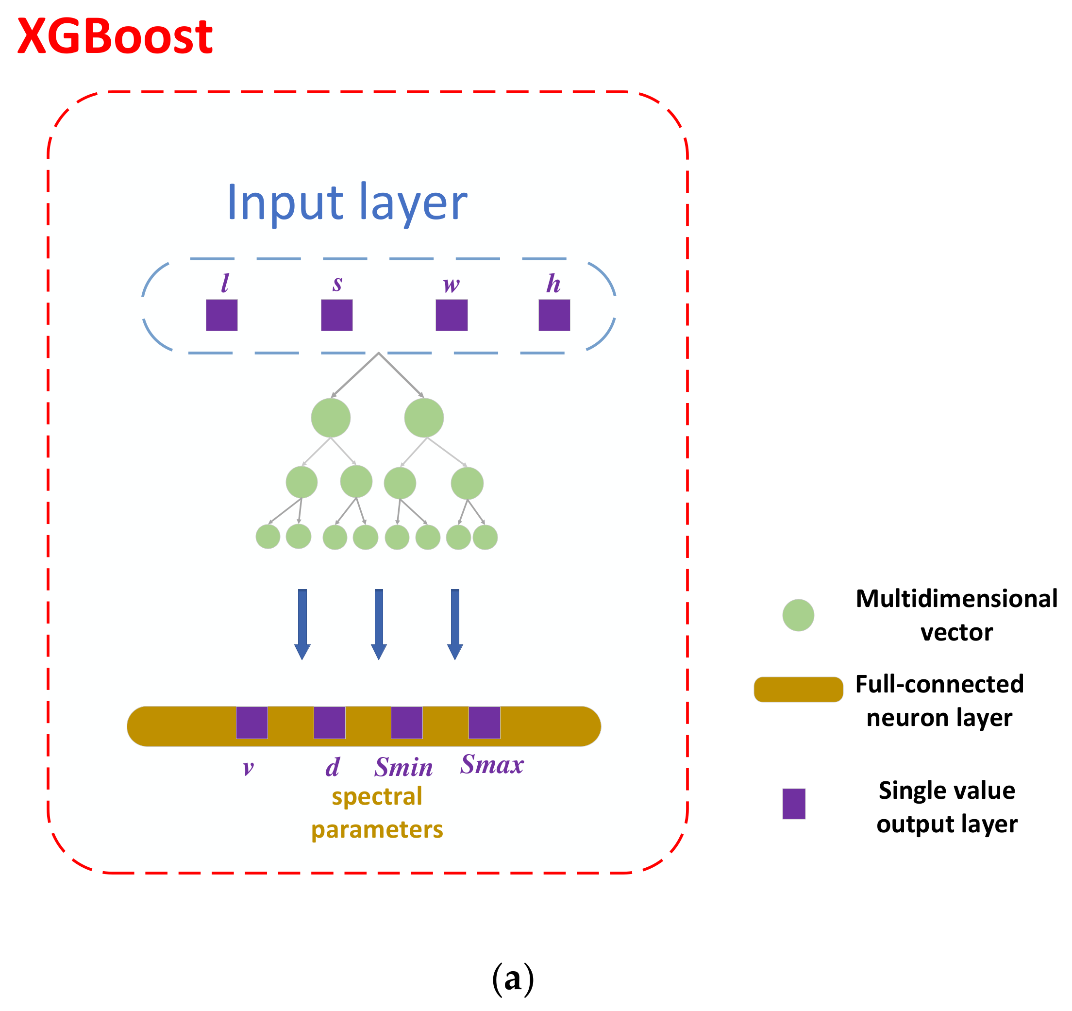
XGBoost is trained to learn the characteristic of MML and inverse design the parameters using the four characteristic parameters v, d, Smin and Smax. The software builds a one-way mapping between the structural and spectral parameters. XGBoost provides similar functionality to that of CST, but has a much faster calculation speed after training with a dataset simulated by CST. It also provides the importance index of structural parameters to the optimization of different spectrum parameters. DNN plays the exact opposite role to XGBoost, offering different structural parameters to the pre-trained XGBoost, which then predicts the spectral parameters of the structural parameters according to the previously established one-way mapping relationship. This process is called inverse design.
XGBoost uses the greedy algorithm to traverse all possible values of the four parameters (s, l, w, h) of the MML structure and calculate the importance index. It then continuously splits the data set according to the importance index to construct a decision tree.
As an integration model of decision trees, the output of XGBoost is the weighted sum of the outputs of the k decision trees. The best split in each tree learning must be determined. In order to do so, a split finding algorithm considers all possible splits on all four structural features, which is called the exact greedy algorithm [21]. The objective function at step t of XGBoost is:
where and are the first and second-order gradient statistics on the loss function (MSE), and is the regularization parameter used to solve the problem of over-fitting by limiting the size of each decision tree output value.
The proposed microstrip meander line predict model (MMLPM) is schematically depicted in Figure 3a. In the learning process of XGBoost, the importance index for all features is calculated according to the formula of the corresponding optimal value [21], where λ is an artificially defined hyperparameter used to control the weight of the regularization parameters, and subscript i represents the set, the data are present according to the split point. Moreover, these indicators will provide a meaningful reference for designers to configure the MML. As shown in Figure 3b, the influence of the metal folding line length on the phase velocity v and transmission Smin is greater than other structural parameters. In the same way, adjusting the value pairs of s is more helpful to improve the performance of d and Smin.
In this paper, 900 samples were simulated by CST to train and validate XGBoost. Based on the results of several previous simulations, s was set to be in the range from 0.01 to 0.03 mm, l was set to be in the range from 0.1 to 0.3 mm, h was set to be in the range from 0.015 to 0.04 mm, w was set to be in the range from 0.015 to 0.04 mm. The entire data set had a total of 900 data points for network learning and verification at ratios of 0.7 and 0.3, respectively.
We use XGBoost to establish the forward mapping relationship between the structural and spectral parameters, which is more interpretable than neural networks. However, our goal is to use deep learning and machine learning to reverse design SWS rather than simply predict the spectrum. Therefore, we also train a fully connected forward neural network (FNN) whose input is a set of spectral parameters and output is a set of structural parameters. Adam optimization algorithm is used [22], which can automatically adapt to adjust the learning rate. As shown in Figure 4a, the basic structure of a DNN consists of three components: An input layer, a hidden layer, and an output layer. These layers are an FCNN, meaning every neuron in one layer is connected to all neurons in the previous layer. Therefore, the output of neurons in the previous layer is the input of neurons in the next layer, and each connection has a weighted value w. In the equations in Figure 4b, σ is the activation function. The goal of each iteration is to update these weights so that the prediction results are increasingly similar to the simulation data. There is no connection between neurons within the same layer. In the learning process of a neural network, losses in learning are propagated backward, and can be measured by the MSE or linear errors.
For a node in a hidden layer of a neural network, the calculation of its activation value is divided into two steps: (1) The values of the nodes x1 and x2 are given when entering the hidden node to achieve a linear transformation, and the value of Z[1] = w1x1 + w2x2 + b[1] = w[1]x + b[1] is calculated, where superscript 1 designates the first hidden layer. (2) For a nonlinear transformation; that is, a nonlinear activation function, the output of the node a(1) = g(z(1)) is caculated, where g(z) is a nonlinear function. Graphs of three of the most commonly used active functions are provided in Figure 4b. All three active functions in our method are tested, and the training loss is shown in Figure 4c. The backpropagation loss of the FNN is calculated from the mean square error function for the output of XGBoost and the input of the FNN [23], which means the FNN is trained to offer XGBoost a suitable set of structural parameters. Once the training is done, the corresponding structure parameters can be obtained by inputting the target spectral parameters to the FNN. Obviously, the results of Tanh and ReLu have larger gradients than that of sigmoid near the center value, leading to faster weight update speed of multi-layer neural network. Although the training error of tanh activation function is minimized, the training losses of ReLu and tanh are very close to each other. Moreover, ReLu can effectively avoid the problem of gradient disappearance in DNN [23]. Therefore, ReLu function is chosen as the active function in our method.
4. Results and Discussion
To validate the XGBoost-DNN, a range of initialization spectral properties were offered to the model, where v was less than 0.15c, d was less than 0.005, Smax was less than −5 dB, Smin was higher than −5 dB. For an SWS with the desired center frequency of 160 GHz and bandwidth of 20 GHz, a set of the specific structural parameters designed by XGBoost-DNN were given as: s = 0.012 mm, l = 0.2 mm, h = 0.02 mm, w = 0.016 mm.
The cold-test and transmission characteristics are shown in Figure 5a,b. As shown in the figure, the maximum reflection of our optimized structure remains below −15 dB from 150 to170 GHz, the phase velocity is 0.134c at the central frequency, and the on-axis coupled pierce impedance at 0.03 mm above the metal MML is 14.3 Ω, which means the optimized structure performs as expected.
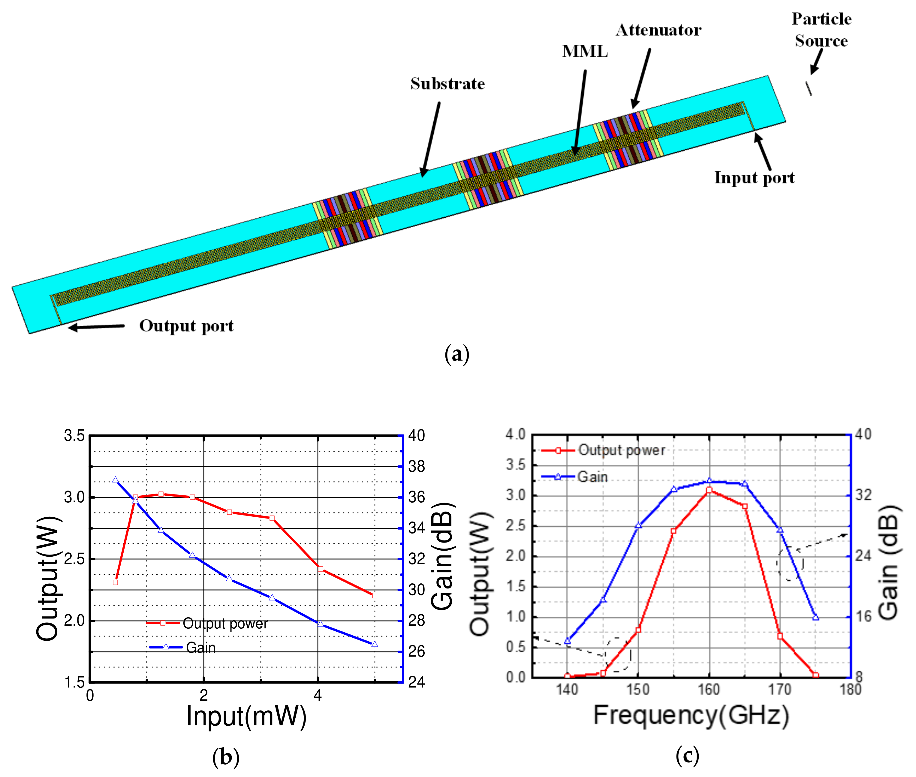
PIC simulation was performed to validate the designed MML-SWS. A 4.59-kV operating voltage and a 0.232 mm × 0.02 mm sheet beam with 50 mA current were applied with a 0.6 T longitudinal magnetic field in the PIC simulation. The schematic model in CST is shown in Figure 6a. In addition, according to the guidance of previous literature [24], three section attenuators with a maximum tangent loss of 0.24 were used, and each attenuator had a length of 15 periods, located at periods 25, 65 and 105, respectively. As shown in Figure 6b, when the input signal power is 1 mW, the stable output power with 180 periods reaches 3 W with 36.66 dB gain at 160 GHz. Meanwhile, the power gain is above 30 dB over a 20 GHz bandwidth range from 150 to 170 GHz with input power at 1 mW, as shown in Figure 6c, which validates that the design geometry meets our requirements.
5. Conclusions
We successfully utilized XGBoost and DNN technology to design an MML-SWS for the optimization of a cold-test and transmission characteristics in this work. The raw data collection was based on the simulation results obtained from CST with four observed parameters of phase velocity at the center frequency, dispersion flatness, minimal transitivity, and maximal reflectivity between the bandwidth. The XGBoost-DNN could learn these relations from the raw data to determine the optimal parameters. Once the center frequency and bandwidth were given, the appropriate SWS could be designed automatically.
In this paper, only D-band parameters were learned by our algorithm. In future work, the learning database will extend the frequency range from the Ka-band to the G-band. Meanwhile, other types of SWSs also could use this methodology to provide a fast and creative technique to research vacuum electronic devices.
Author Contributions
Conceptualization, N.B., Y.Z. and X.S.; methodology, Y.Z. and N.B.; software, Y.Z.; validation, Y.Z. and Y.X.; investigation, Y.Z. and Y.X.; resources, Y.Z. and Y.X.; data curation, Y.Z. and Y.X.; writing—original draft preparation, Y.Z. and Y.X.; writing—review and editing, N.B. and X.S.; supervision, N.B. and X.S.; project administration, N.B.; funding acquisition, N.B. All authors have read and agreed to the published version of the manuscript.
Funding
This research was funded by the National Natural Science Foundation of China, grant number 61871110. The APC was funded by Southeast University.
Conflicts of Interest
The authors declare no conflict of interest.
References
- Lee, Y.L.; Qin, D.; Wang, L.C.; Sim, G.H. 6G Massive Radio Access Networks: Key Applications, Requirements and Challenges. IEEE Open J. Veh. Technol. 2021, 2, 54–66. [Google Scholar] [CrossRef]
- Shiffler, D.; Nation, J.A.; Schachter, L.; Ivers, J.D.; Kerslick, G.S. Review of high power traveling wave tube amplifiers. In Proceedings of the IEEE MTT-S Microwave Symposium Digest, Albuquerque, NM, USA, 1–5 June 1992. [Google Scholar]
- Gong, Y.B.; Zhou, Q.; Hu, M.; Zhang, Y.H.; Li, X.Y.; Gong, H.R.; Wang, J.X.; Liu, D.W.; Liu, Y.H.; Duan, Z.Y.; et al. Some Advances in Theory and Experiment of High-Frequency Vacuum Electron Devices in China. IEEE Trans. Plasma Sci. 2019, 47, 1971–1990. [Google Scholar] [CrossRef]
- Ryskin, N.M.; Torgashov, R.A.; Starodubov, A.V.; Rozhnev, A.G.; Serdobintsev, A.A.; Pavlov, A.M.; Galushka, V.V.; Bessonov, D.A.; Ulisse, G.; Krozer, V. Development of microfabricated planar slow-wave structures on dielectric substrates for miniaturized millimeter-band traveling-wave tubes. J. Vac. Sci. Technol. B 2021, 39, 013204. [Google Scholar] [CrossRef]
- Paoloni, C.; Gamzina, D.; Letizia, R.; Zheng, Y.; Luhmann, N.C., Jr. Millimeter wave traveling wave tubes for the 21st Century. J. Electromagn. Waves Appl. 2021, 35, 567–603. [Google Scholar] [CrossRef]
- Billa, R.B.L.R.; Rao, J.M.; Letizia, R.; Paoloni, C. Design of D-band Double Corrugated Waveguide TWT for Wireless Communications. In Proceedings of the 2019 International Vacuum Electronics Conference (IVEC), Busan, Korea, 28 April–2 May 2019. [Google Scholar]
- Sumathy, M.; Datta, S.K. Design and Characterization of a W-Band Folded-Waveguide Slow-Wave Structure. J. Infrared Milli Terahz. Waves 2017, 38, 538–547. [Google Scholar] [CrossRef]
- Starodubov, V.; Serdobintsev, A.A.; Pavlov, A.M.; Galushka, V.V.; Mitin, D.M.; Ryskin, N.M. A novel microfabrication technology of planar microstrip slow-wave structures for millimeter-band traveling-wave tubes. In Proceedings of the IEEE International Vacuum Electronics Conference (IVEC), Monterey, CA, USA, 24–28 April 2018; pp. 333–334. [Google Scholar]
- Ryskin, N.M.; Rozhney, A.G.; Starodubov, A.V.; Serdobintsev, A.A.; Pavlov, A.M.; Benedik, A.I.; Torgashov, R.A.; Torgashov, G.B.; Sinitsyn, N.I. Planar Microstrip Slow-Wave Structure for Low-Voltage V-Band Traveling-Wave Tube With a Sheet Electron Beam. IEEE Electron. Device Lett. 2018, 39, 757–760. [Google Scholar] [CrossRef]
- Torgashov, R.A.; Ryskin, N.M.; Rozhnev, A.G.; Serdobintsev, A.A.; Pavlov, A.M.; Galushka, V.V.; Bakhteev, I.S.; Molchanov, S.Y. Theoretical and Experimental Study of a Compact Planar Slow-Wave Structure on a Dielectric Substrate for the W-Band Traveling-Wave Tube. Tech. Phys. 2020, 65, 660–665. [Google Scholar] [CrossRef]
- Wen, Z.; Luo, J.; Li, Y.; Guo, W.; Zhu, M. A Concentric Arc Meander Line Slow Wave Structure Applied on Low Voltage and High Efficiency Ka-Band TWT. IEEE Trans. Electron Devices 2021, 68, 1262–1266. [Google Scholar] [CrossRef]
- Specht, D.F. A general regression neural network. IEEE Trans. Neural Netw. 1991, 2, 568–576. [Google Scholar] [CrossRef] [PubMed] [Green Version]
- LeCun, Y.; Bengio, Y.; Hinton, G. Deep learning. Nature 2015, 521, 436–444. [Google Scholar] [CrossRef]
- Tahersima, M.H.; Kojima, K.; Koike-Akino, T.; Jha, D.; Wang, B.N.; Lin, C.W.; Parsons, K. Deep Neural Network Inverse Design of Integrated Photonic Power Splitters. Sci. Rep. 2019, 9, 1368. [Google Scholar] [CrossRef] [PubMed]
- Lin, R.H.; Zhai, Y.F.; Xiong, C.X.; Li, X.H. Inverse design of plasmonic metasurfaces by convolutional neural network. Opt. Lett. 2020, 45, 1362–1365. [Google Scholar] [CrossRef] [PubMed]
- Hegde, R.S. Deep Learning: A new tool for photonic nanostructure design. Nanoscale Adv. 2020, 2, 1007–1023. [Google Scholar] [CrossRef]
- Ma, W.; Liu, Z.; Kudyshev, Z.A.; Boltasseva, A.; Cai, W.S.; Liu, Y.M. Deep learning for the design of photonic structures. Nat. Photonics 2021, 15, 77–90. [Google Scholar] [CrossRef]
- Ma, W.; Cheng, F.; Liu, Y.M. Deep-Learning-Enabled On-Demand Design of Chiral Metamaterials. ACS Nano 2018, 12, 6326–6334. [Google Scholar] [CrossRef] [PubMed]
- Alagappan, G.; Png, C.E. Deep learning models for effective refractive indices in silicon nitride waveguides. J. Opt. 2019, 21, 035801. [Google Scholar] [CrossRef]
- Malkiel, I.; Mrejen, M.; Nagler, A.; Arieli, U.; Wolf, L.; Suchowski, H. Deep learning for the design of nano-photonic structures. In Proceedings of the 2018 IEEE International Conference on Computational Photography (ICCP), Pittsburgh, PA, USA, 4–6 May 2018; pp. 1–14. [Google Scholar]
- Chen, T.; Guestrin, C. XGBoost: A Scalable Tree Boosting System. In Proceedings of the 22nd ACM SIGKDD International Conference on Knowledge Discovery and Data Mining, San Francisco, CA, USA, 13–17 August 2016; pp. 785–794. [Google Scholar]
- Yi, D.; Ahn, J.; Ji, S.M. An Effective Optimization Method for Machine Learning Based on ADAM. Appl. Sci. 2020, 10, 1073. [Google Scholar] [CrossRef] [Green Version]
- Rumelhart, D.; Hinton, G.; Williams, R. Learning representations by back-propagating errors. Nature 1986, 323, 533–536. [Google Scholar] [CrossRef]
- Guo, G.; Wei, Y.; Zhang, M.; Travish, G.; Yue, L.; Xu, J.; Yin, H.; Huang, M.; Gong, Y.; Wang, W. Novel Folded Frame Slow-Wave Structure for Millimeter-Wave Traveling-Wave Tube. IEEE Trans. Electron. Devices 2013, 60, 3895–3900. [Google Scholar] [CrossRef]
Figure 1.
(a) Front view; and (b) top view of the MML unit structure.


Figure 2.
Cold-test characteristic of the MML structure: (a) Dispersion characteristic; (b) Transmission (S21) and reflection (S11).
Figure 2.
Cold-test characteristic of the MML structure: (a) Dispersion characteristic; (b) Transmission (S21) and reflection (S11).

Figure 3.
(a) MMLPM basic structure; (b) the corresponding optimal value with phase velocity; (c) the corresponding optimal value with phase velocity flatness; (d) the corresponding optimal value with Smax; (e) the corresponding optimal value with Smin.
Figure 3.
(a) MMLPM basic structure; (b) the corresponding optimal value with phase velocity; (c) the corresponding optimal value with phase velocity flatness; (d) the corresponding optimal value with Smax; (e) the corresponding optimal value with Smin.


Figure 4.
(a) XGBoost-DNN composite structure; (b) basic structure of a fully connected deep neural network; (c) three different active functions; (d) training loss with different active functions.
Figure 4.
(a) XGBoost-DNN composite structure; (b) basic structure of a fully connected deep neural network; (c) three different active functions; (d) training loss with different active functions.

Figure 5.
(a) Transmission characteristics from 150 to 170 GHz of the designed MML-SWS; (b) dispersion characteristic and coupled impedance of the structure.
Figure 5.
(a) Transmission characteristics from 150 to 170 GHz of the designed MML-SWS; (b) dispersion characteristic and coupled impedance of the structure.

Figure 6.
(a)Schematic model for PIC simulation; (b) output power and gain versus input signal power; (c) output power and gain versus frequency.
Figure 6.
(a)Schematic model for PIC simulation; (b) output power and gain versus input signal power; (c) output power and gain versus frequency.

Publisher’s Note: MDPI stays neutral with regard to jurisdictional claims in published maps and institutional affiliations. |
© 2021 by the authors. Licensee MDPI, Basel, Switzerland. This article is an open access article distributed under the terms and conditions of the Creative Commons Attribution (CC BY) license (https://creativecommons.org/licenses/by/4.0/).
Share and Cite
MDPI and ACS Style
Zhu, Y.; Xie, Y.; Bai, N.; Sun, X. Inverse Design of a Microstrip Meander Line Slow Wave Structure with XGBoost and Neural Network. Electronics 2021, 10, 2430. https://0-doi-org.brum.beds.ac.uk/10.3390/electronics10192430
AMA Style
Zhu Y, Xie Y, Bai N, Sun X. Inverse Design of a Microstrip Meander Line Slow Wave Structure with XGBoost and Neural Network. Electronics. 2021; 10(19):2430. https://0-doi-org.brum.beds.ac.uk/10.3390/electronics10192430
Chicago/Turabian StyleZhu, Yijun, Yang Xie, Ningfeng Bai, and Xiaohan Sun. 2021. "Inverse Design of a Microstrip Meander Line Slow Wave Structure with XGBoost and Neural Network" Electronics 10, no. 19: 2430. https://0-doi-org.brum.beds.ac.uk/10.3390/electronics10192430
Note that from the first issue of 2016, this journal uses article numbers instead of page numbers. See further details here.