
Improving LCC Series-Based Wireless Power Transfer System Output Power at High Temperature


1
Graduate School of Engineering Science and Technology (Doctorial Program), 123 University Road, Section 3, Douliu 64002, Taiwan
2
Department of Electrical Engineering, National Yunlin University of Science and Technology, Douliu 64002, Taiwan
*
Author to whom correspondence should be addressed.
Electronics 2021, 10(22), 2875; https://0-doi-org.brum.beds.ac.uk/10.3390/electronics10222875
Submission received: 28 October 2021
/
Revised: 17 November 2021
/
Accepted: 18 November 2021
/
Published: 22 November 2021
(This article belongs to the Special Issue Advances in Wireless Power Transfer and Applications)
Abstract
:Adding a core to a coupling coil can improve transmission efficiency. However, the added core causes the self-inductance of the coupling coil to increase at a high temperature due to the temperature-sensitive property of the core material’s permeability. The self-inductance increases, causing the resonance frequency to shift down, thereby decreasing the output power. The 3 dB bandwidth of the system can learn of the correspondence between the output power and the resonance frequency. In order to make sure that the output power does not excessively decrease at a high temperature, this study employs a simulation for the LCC-S-based wireless power transfer system. Adding a minor resistance to shift down the lower cutoff frequency ensures that the resonance frequency yielded by the temperature rise can be higher than the lower cutoff frequency, making the output power higher than half of the maximum. Then, an adjustment on the compensation capacitances on the resonant circuit elevates the output power more. The outcomes are consistent with the prediction. Adding the core to the coupling coil improves transmission efficiency; increasing the bandwidth of the system excessively decreases the output power decline at a high temperature for the temperature-sensitive core material permeability.
1. Introduction
Adding a core to a coupling coil increases the transmission efficiency of a wireless power transfer system [1,2,3], but this effect decreases at high temperatures [4]. This is due to the temperature-sensitive property of the core material’s permeability. The permeability increases with temperature, increasing the coupling coil’s self-inductance while decreasing the resonance frequency. Because wireless power transfer technology is used in various applications at diverse temperatures, supplying power evenly to the load is vital.
Many studies have shown that adding a core to the coupling coil can increase its self-inductance, elevating the quality factor of the coupling coil by the increase in the self-inductance, which then enhances the efficiency [5,6]. However, because the core material’s permeability is temperature sensitive, the self-inductance of the coupling coil changes with the temperature. When the compensation capacitance is immovable, the resonance frequency varies with the temperatures. There is a sharp decrease in the output power once the new resonance frequency is out of the effective range of the bandwidth. Thus, the bandwidth of the resonant circuit plays a vital role.
For the self-inductance of the coupling coil to increase at a high temperature, the classical series/parallel resonant circuit with a single component will also have an identical encounter. Increasing the driving voltage without the modification on the circuit is a way to elevate the power at a high temperature [7], but this will exceed the rating of the high driving voltage at room temperature. In this case, this adds a minor resistance to the circuit, the system’s 3 dB bandwidth can be widened as expected, rendering the output power at a high temperature higher than half of the maximum, but the output power decreases with the resistance increases. Alternatively, the compensation capacitance can be adjusted to accord with the new resonance frequency caused by the temperature rises. The act of capacitance adjustment would lead to the maximum output power appearing at a high temperature, while the output power at room temperature is considerably low.
In capacitive wireless power transfer technology, the power transfer counts on the planes by an electric field. The technology transfers energy by capacitive coupler planes without the addition of a core similar to a magnetic field. Therefore, there is no concern regarding the temperature-sensitive permeability of the core material; the temperature would only have a minor impact on the capacitive wireless power transfer technology. However, there are several limitations to capacitive wireless power transfer technology [8]. As far as the plate voltage is concerned, when achieving the desired power density with a certain extent in the case of a small coupler dimension, the plate voltage applied to the plate could be considerably high, because a system with a low voltage is hard to achieve. Capacitive wireless power transfer technology is appropriate for short coupling distances and large coupling areas.
We increased the output power of an inductor–capacitor–capacitor resonant circuit and a series receiving circuit (LCC-S) wireless power transfer system [9,10,11] operating at high temperatures by increasing the bandwidth.
We increased the series resistance of the LCC resonant circuit to increase the bandwidth according to circuit theory and adjusted the capacitance to increase the output power level.
The ratio between the series and parallel capacitance values of the LCC resonant circuit affects the magnitude of coupling and drive currents [12]. When the series and parallel capacitance values are equal, the coil current is twice the strength of the drive current, while decreasing the capacitance ratio increases the coil current. At high temperatures, increasing the circuit resistance raises the output power.
2. LCC Series-Compensated Topology and Effect of Temperature
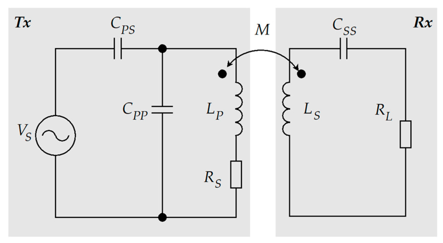
The LCC-S compensation topology is a variant of the series/parallel combination resonant circuit; its structure is presented in Figure 1.
In this topology, the transmitter (Tx) employs an LCC resonant circuit with two compensated capacitors. The resonant current flowing into the coupling coil is twice the strength of the drive current. Both compensated capacitors have identical capacitance.
The LCC resonant circuit in the compensation topology and the current ratio between the coil and the drive currents, γ, as mentioned above, gives the following according to a previous paper [13]:
Here, IS represents the drive current supplied from the drive source. The coil current would be twice as strong as mentioned above if the two compensation capacitances are equal.
The series circuit in the receiver (Rx) comprises a series-compensated capacitor connected to the Rx coupling coil and the load. When the LCC-S-compensated topology is in the state of resonance, the reflected impedance of the Rx series circuit only has the real part of reflected resistance and not the imaginary part of reflected reactance.
The frequency for tuning the LCC-S-compensated topology to resonance can be calculated as follows [14]:
where LP and LS represent the self-inductance of the coupling coil on Tx and Rx, respectively; the CPS and CPP are the series and parallel capacitances on the LCC resonant circuit. The M represents the mutual inductance.
With regard to the resonance frequency for the Tx, its expression is held by the following calculations presented below. The total impedance on the LCC resonant circuit, ZT, neglecting parasitic resistance, is represented as
For the resonance, it is necessary for the imaginary part of the circuit to be zero. Thus, ZT can be shown as
With the calculated results for the LP and CPP, the equation for the ZT becomes
Then,
The expression for the LCC resonance frequency holds, therefore, by the mathematical proceeding above.
The self-inductance depends on the dimensions of the core, the number of turns in the winding, and the permeability of the core material:
In the expression for the self-inductance, μ represents the permeability of the core material and the part of the flux path in the air; N is the number of turns in the winding. Although the core dimension includes a core cross-section, A, and core length, l, both are reciprocal.
Core permeability is sensitive to temperature; a discrepancy in the temperature in different parts of the core results in the core having varying permeabilities, thereby altering the value of self-inductance. As described in the literature, the effective permeability of the core µe on the coupling coil changes with the temperature coefficient TC and the temperature factor TF. As described in the literature, the effective permeability of the core on the coupling coil changes with the temperature coefficient and the temperature factor. The relationship between µe, TC, and TF is given as follows:
Herein, the temperature coefficient is defined as the change in the initial magnetic permeability per degree Celsius. The temperature factor is defined as the value of the temperature coefficient per unit of magnetic permeability. The effective magnetic permeability of the core at various temperatures will suffer as a result of these two properties.
The relationship between the self-inductance, L, and the effective magnetic permeability, µe, is given as follows:
where L is the self-inductance, le is the effective length of the core, N is the number of turns, and Ae is the effective cross-section of the core.
The effective permeability is nearly proportional to the self-inductance. The self-inductance would change with the variation in effective permeability at different temperatures in the case of the coil geometry being identical.
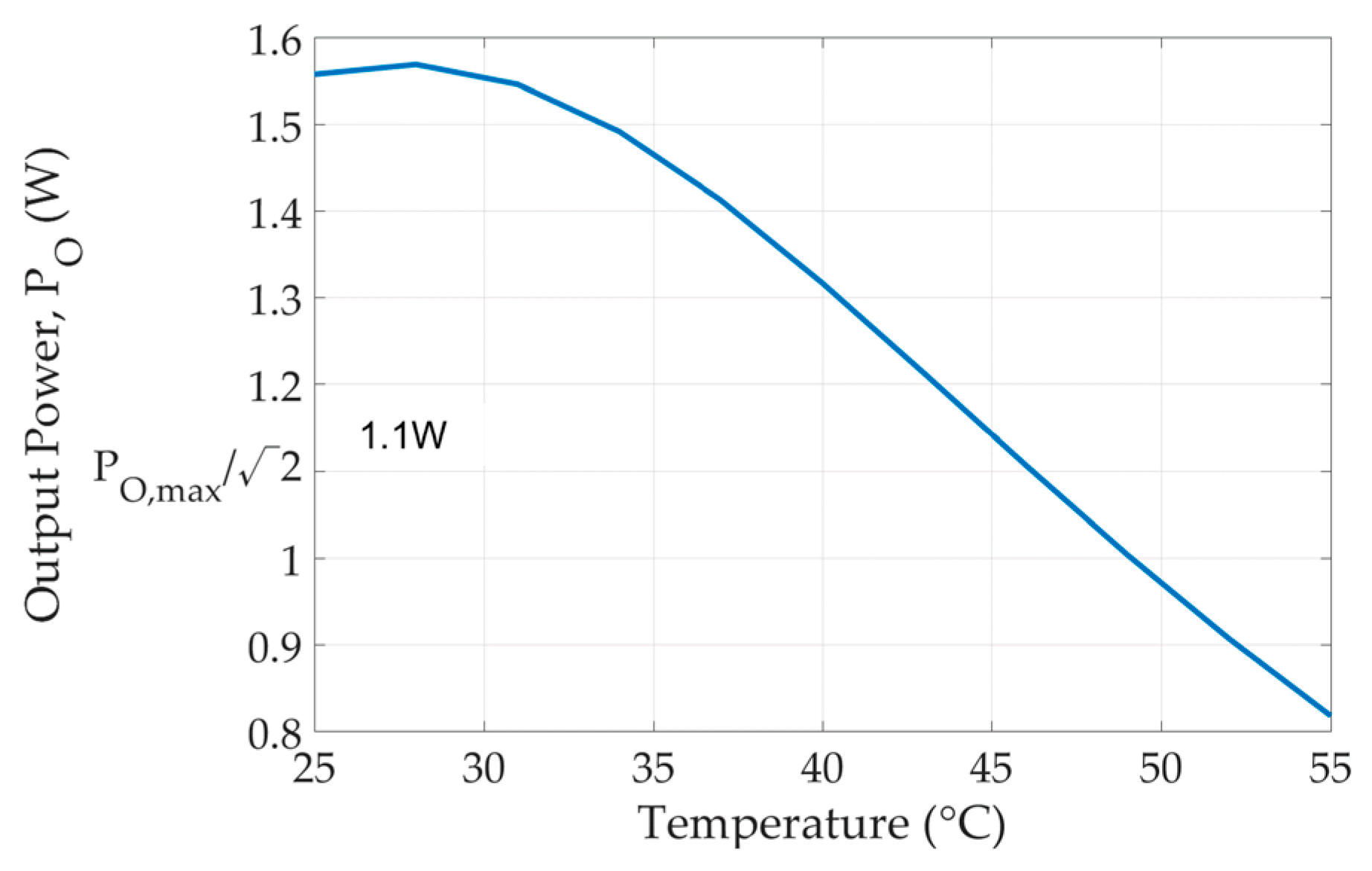
The resonance frequency of the topology is inversely proportional to the square root of the inductance and capacitance product, as shown in Equation (2). The variation in the inductance caused by the temperature results in an inconsistent resonance frequency. For a given drive frequency, the output power greatly decreases with increasing temperature. The output power variation with the temperature is depicted in Figure 2.
An increase in the temperature results in a sharp decrease in output power; this is caused by the deviation between the driving and topology resonance frequencies—the increase in the temperature increases the permeability of the core material, further increasing the self-inductance of the coupling coil. The increased self-inductance decreases the resonance frequency, resulting in a deviation from the original frequency of the drive source.
The output power PO depends on the frequency, the coil current of the Tx, and the circuit quality factor of the Rx:
The Rx circuit quality factor QS can be expressed as Equation (11). The quality factor of the Rx circuit in the case of neglecting the parasitic resistance of the circuit is proportional with the frequency, ω, and self-inductance on the Rx circuit, LS, while being in inverse proportion with the internal resistance of the coupling coil winding, R. Regarding the internal resistance R, that is the resistance of the wire for the coupling coil winding. Its magnitude involves the power dissipation of the coupling coil.
Combining Equations (10) and (11) reveals the square relationship between the output power and resonance frequency, indicating that an increased frequency deviation between the driving and topology resonance frequencies results in an increased decline in the output power.
Furthermore, the coil current IL can be derived through mesh current analysis:
where ZP is the impedance; this represents the series of the self-inductance of the Tx coil and the reflected impedance ZR from the Rx:
The reflected impedance [15,16,17] ZR of the Rx series circuit can be calculated as follows:
where M is mutual inductance, given as
The variable k in Equation (15) is the coupling coefficient between the coupling coils on the Tx and Rx. Because these parameters are relative to the leakage flux of the coils, the coupling coefficient is related to the coil geometries and the coupling distance between the two coils. Its magnitude involves the mutual inductance between the two coupling coils on the Tx and Rx. The maximum coupling coefficient is 1.
The system transfer function that holds based on Equation (12) would be expressed as follows:
The coefficients in the transfer function are
and
The frequency of the drive source for tuning the wireless power transfer system into a state of resonance depends on the inductance and capacitance at room temperature. As explained earlier, for a given frequency of the drive source, the self-inductance of the coupling coil increases with temperature, resulting in the resonance frequency shifting to another frequency point and yielding the deviation in the case of a fixed frequency of the drive source.
The new resonance frequency caused by the increased inductance ωO,H can be expressed as follows:
where ΔL is the increase in the inductance.
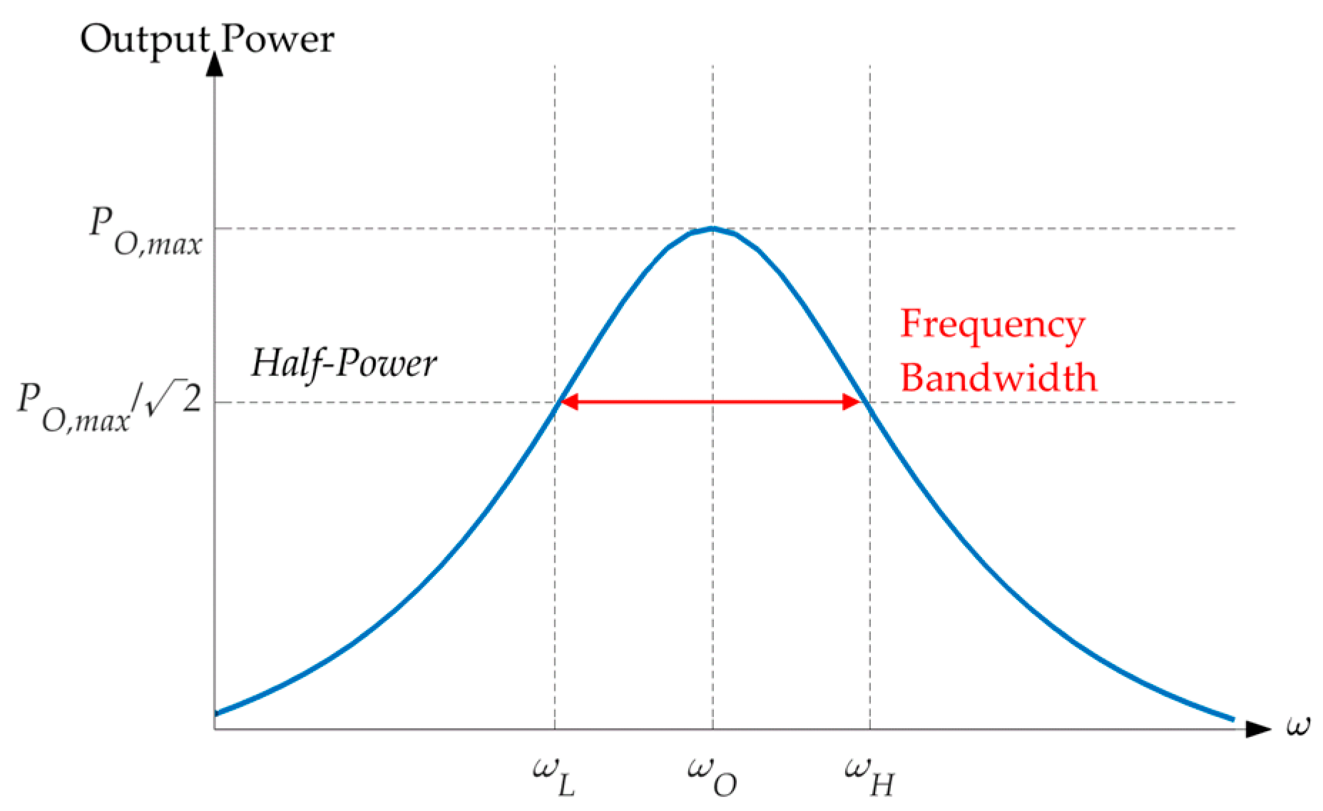
If ωO,H is within the allowance of the bandwidth, the output power is more than half of the full power at least. The output power decreases notably once ωO,H is out of the bandwidth. To compensate for the loss in output power at high temperatures, the bandwidth can be increased so that the new resonance frequency is within the bandwidth.
The bandwidth BW is defined as the band between two half-power frequencies:
As far as the resonant circuit is concerned, it will transfer the power to the receiving side to supply the load within the specific frequency range. The maximum magnitude of the transfer power should be centered on the resonance frequency. The cutoff frequencies correspond to the power being reduced by three decibels (dB) from its maximum, and they have two lower and two upper cutoff frequencies. As previously stated, bandwidth is defined as the difference between the lower and upper cutoff frequencies. The transfer power will decrease once the frequency exceeds the cutoff frequency.
Figure 3 illustrates the corresponding relationships between the output power and the frequency. In it, ωO represents the resonant frequency; ωH and ωL are the upper and lower cutoff frequencies, respectively.
In addition, Q in Equation (20) represents the quality factor for the circuit of the entire system. According to a previous study [18], the definition for the quality factor of the system circuit is Equation (21). Differing from the QS, the Q here represents the quality factor as far as the entire system is concerned, while QS is only a quality factor for the coil on the Rx circuit.
The bandwidth can be increased by decreasing the circuit quality factor Q. The effect of parasitic resistance on Q is negligible. The resistance can be increased by adding a discrete resistor, RS, between the coupling coil and the ground.
Figure 4 shows how bandwidth BW and output power PO vary with respect to series resistance RS. By varying the load on the wireless power transfer system, the expected power can be obtained without adding a discrete resistance, but the resulting bandwidth is narrow. By contrast, upon adding the resistance, the bandwidth increases, but the output power decreases.
As explained earlier, the output power is proportional to the coil current. According to Equation (12), the coil current depends on the series and parallel capacitances; increasing the series capacitance or decreasing the parallel capacitance increases the coil current, resulting in increased output power.
With regard to the addition of the series resistance and the adjustment of the compensation capacitance, the following discriminant can be utilized:
The above discriminant aims at selecting the compensation capacitances, making a corresponding resonance frequency that can be within the bandwidth when the temperature rises. Here, the bandwidth allowance range is determined by the series resistance used. The bandwidth allowance range will vary with the magnitude of the series resistance. In high temperatures, the appropriate bandwidth for the resonance frequency, as well as the series resistance, is critical. In the discriminant, μO and μT represent the permeability of the core material in the coupling coil at the original and the highest temperatures, respectively. Moreover, α represents the geometry of the coupling coil, comprising the effective cross-section and the length of the core, as well as the number of turns in the winding.
Moreover, the compensation capacitance also affects the frequency of the drive source. Only the correct capacitance in conjunction with the self-inductance of the coupling coil can make the resonance and drive source frequencies consistent or approach consistency, supplying maximum power to the load. Increasing the series resistance would also result in system losses; excessive resistance would increase dissipation. As long as the resonance frequency of the high temperature is within the bandwidth, it is sufficient.
In the next section, the simulation for determining the optimum solution for the LCC-S-compensated topology operated at high temperatures is discussed.
3. Simulation Results
In this section, we build a simulation model using MATLAB based on Figure 1, and the relevant parameters for the components are listed in Table 1. In terms of temperature simulation, the sweep range for the temperature in this simulation is defined as starting at 25 °C and ending at 55 °C. Moreover, the permeability of the core material is assumed to be 6000 H/m at 25 °C and 6050 H/m at 50 °C; 50 H/m increased completely throughout the temperature sweep range.
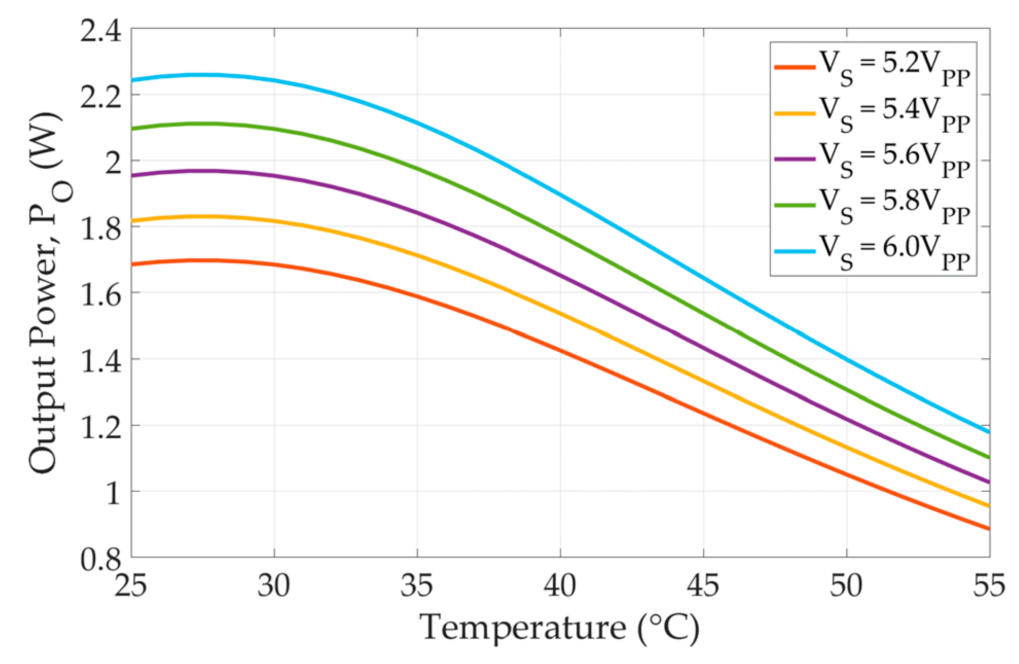
Since the output power sharply decreases with temperature, according to the relationship between the load current IL and the drive voltage VS that in Equation (12), increasing the drive voltage can increase the load current, which can also increase the output power. At high temperatures, when the drive voltage is increased to 6 VPP, the output power may be greater than the original drive voltage. Although the output power can be increased relative to the drive voltage, the output power at a higher drive voltage exceeds the rated power, which may also cause damage to the load due to the excessive output power.
Figure 5 depicts the comparison of the output power with different drive voltages at different temperatures. As previously stated, the output power gradually increases with the drive voltage. At 25 °C, however, the output power exceeds the rated power. At the same load, the current flowing into the load increases sharply; this would damage the load if the current exceeded the rated current of the load.
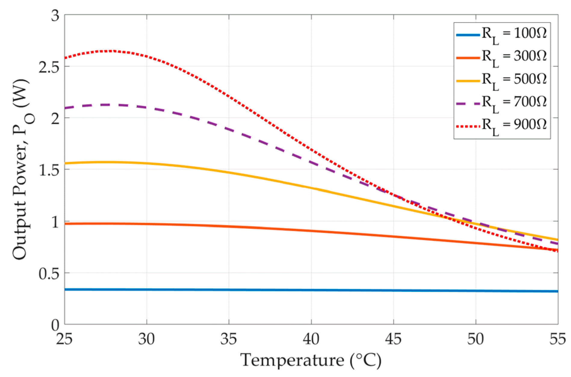
Similarly, in Equation (12), the load current and the reflected impedance have a relationship with the reciprocal, whereas the reflected impedance includes the load in the receiving circuit as Equation (14). Theoretically, increasing the load resistance could increase the load current.
The output power demonstrated in the simulated result would increase with an increase in the load resistance, and more resistance will lead to more output power. However, at a high temperature, the output power is still low, even lower than the original resistance of the load, as shown in Figure 6.
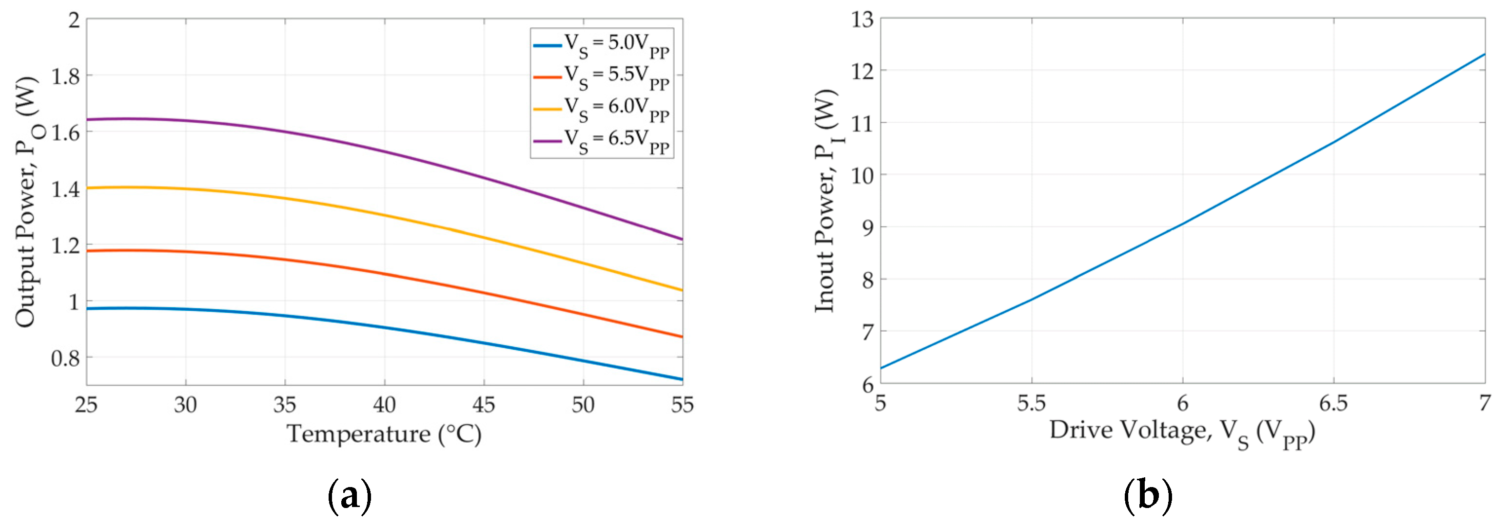
Furthermore, the simulated results show that a reduction in load resistance can mitigate the falling slope during the temperature rise. The output power is nearly 1 W for a load resistance of 300 Ω. As a result, increasing the drive voltage can boost the output power and make it more uniform as the temperature rises. However, the input power will also be increased. A variation with the temperature for different drive voltages in the case of the load resistance of 300 Ω is shown in Figure 7a; the input power variation with the drive voltage increasing is shown in Figure 7b.
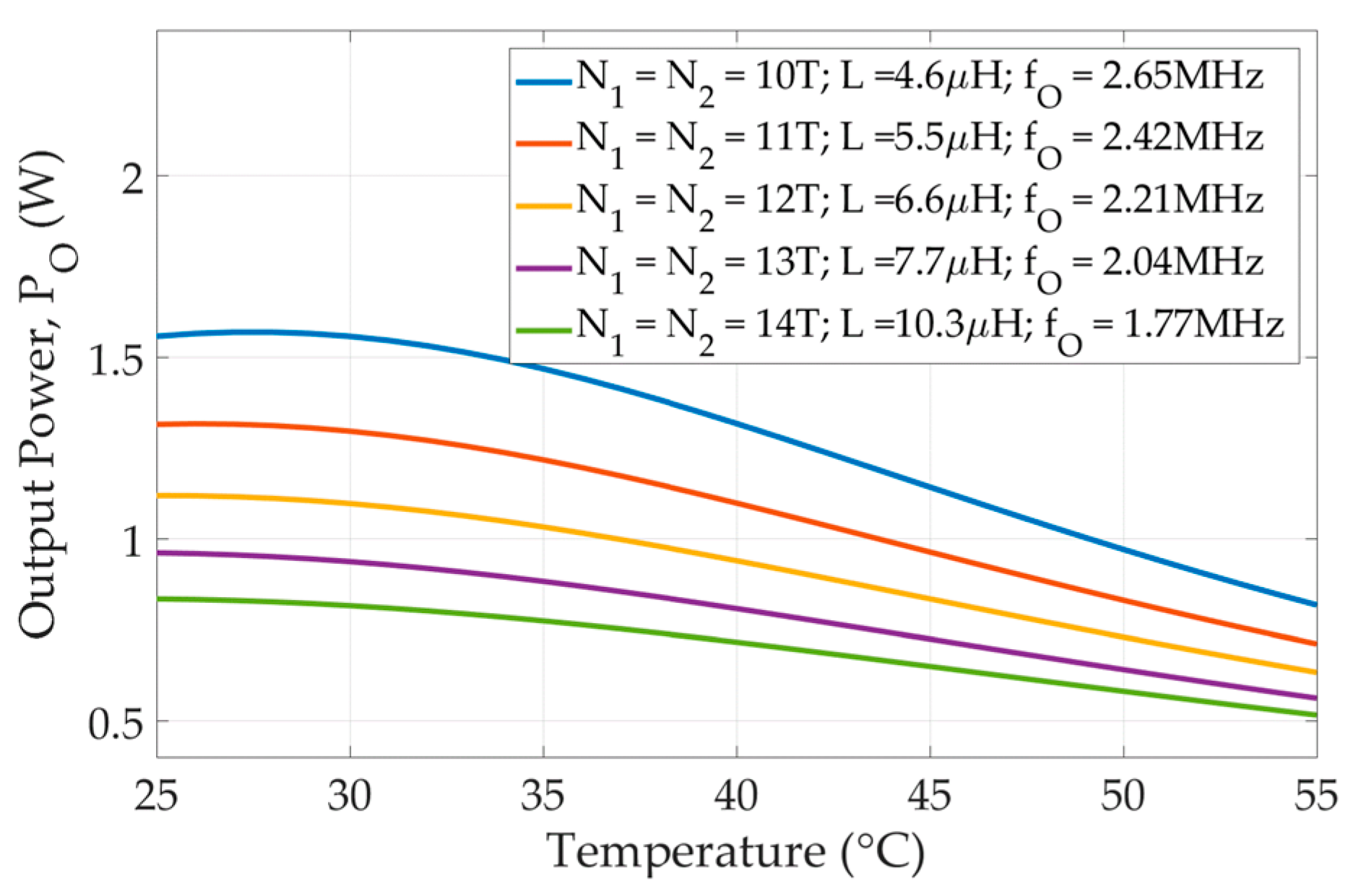
According to Equations (4) and (10), it is found that the output power and mutual inductance are proportional; increasing the number of turns of both coupling coils simultaneously serves to increase the mutual inductance. However, the simulated result shows that the output power decreases as the number of turns increases; the result is shown in Figure 8.
This is because increasing the number of turns will simultaneously increase the impedance of the coupling coil; the output power will still decrease if the drive voltage maintains the original voltage.
The simulation is based on MATLAB according to the circuit structure presented in Figure 1 and the parameter values presented in Table 1.
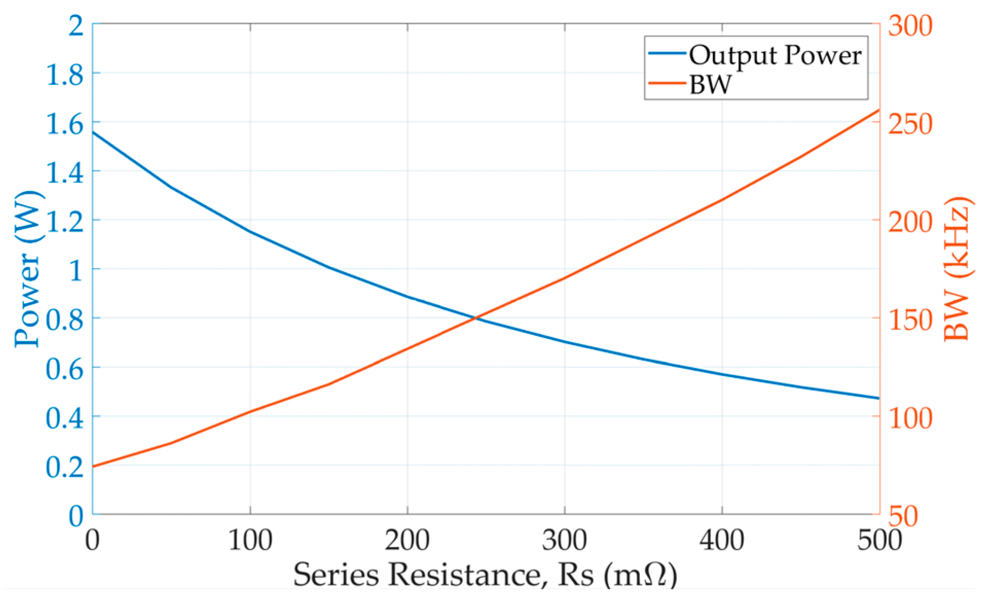
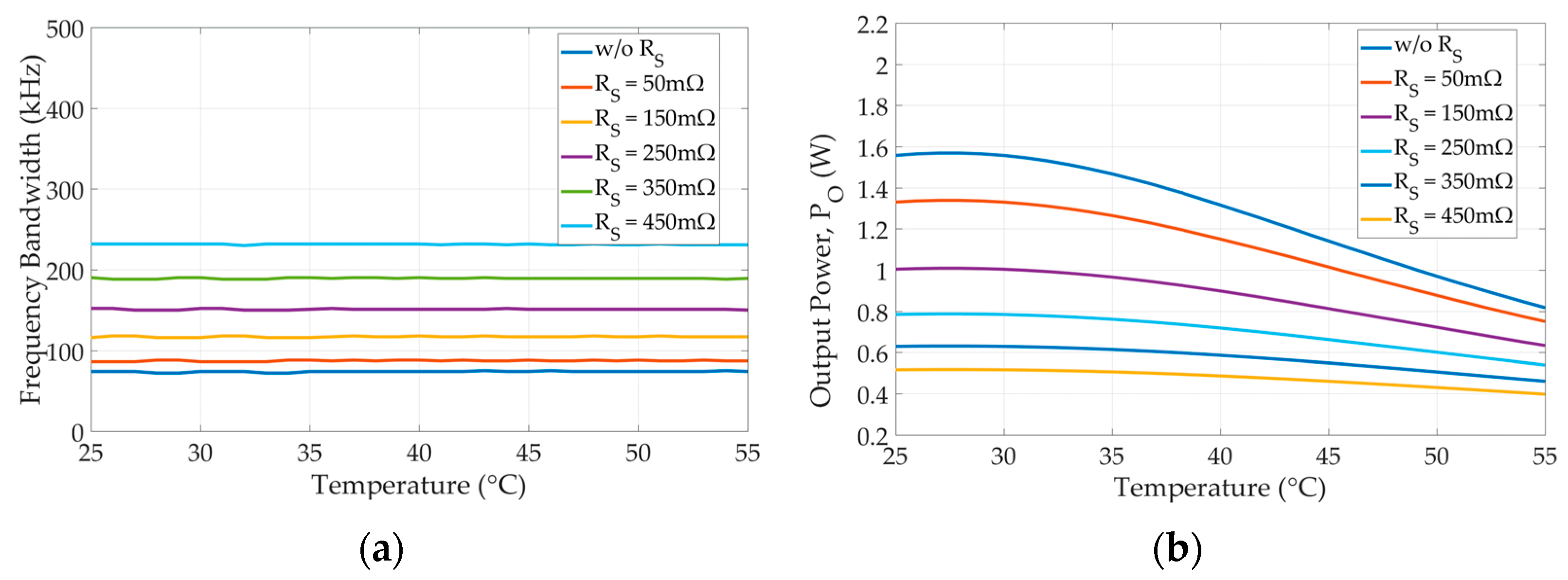
Table 1 lists the parameters of the LCC-S-based wireless power transfer system. As already discussed, the bandwidth can be increased by increasing the series resistance to enhance the output power at high temperatures. The bandwidth and the output power for different series resistance values are shown in Figure 9.
As depicted in Figure 9a, without a series resistor attached in the original design, the so-called w/o RS in the figure, the bandwidth is only approximately 74 kHz. In contrast, the series RS connection into the resonant circuit, corresponding to the bandwidth, is widened; more resistance results in a wider bandwidth. By increasing the series resistance to 450 m, the bandwidth can be increased to 200 kHz. Because of the series RS, the output power for the load would be reduced relative to that before. Figure 9b depicts how the output power would decrease with the addition of a series RS. However, the falling slope for the output power also reduces as the series resistance increases.
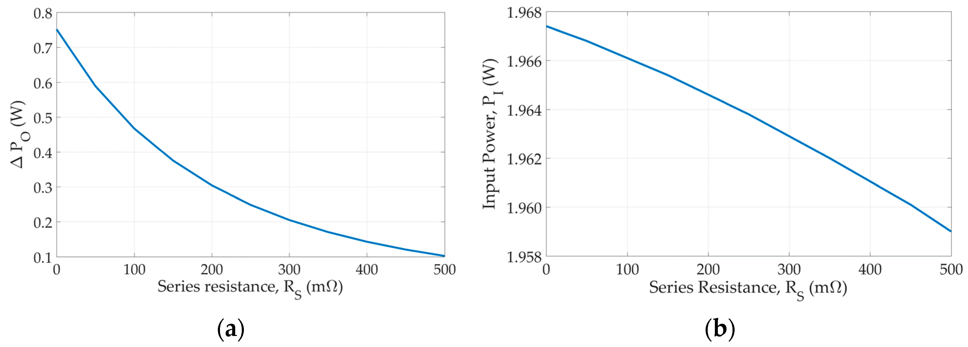
The variance of the output power of the amount of series resistance is demonstrated in Figure 10a. The original design, without the series resistor, has a greater difference in output power as the temperature rises from 25 °C to 55 °C, resulting in a sharp drop in power as the temperature rises. In contrast, the attached series resistor reduces the difference, thereby mitigating the output power decline. As shown in Figure 10b, increasing the series resistance has no significant effect on the input power.
The permeability of the core increases with increasing temperature. In this simulation, the equivalent coil inductance was 4.64 μH, with a 0.04 μH increment, resulting in the resonance frequency of the system being shifted down by 10 kHz. The simulation results revealed that the bandwidth obtained using a series resistance of 450 mΩ was sufficient to include the new frequency point within the bandwidth. However, the output power PO was only 0.5 W at room temperature.
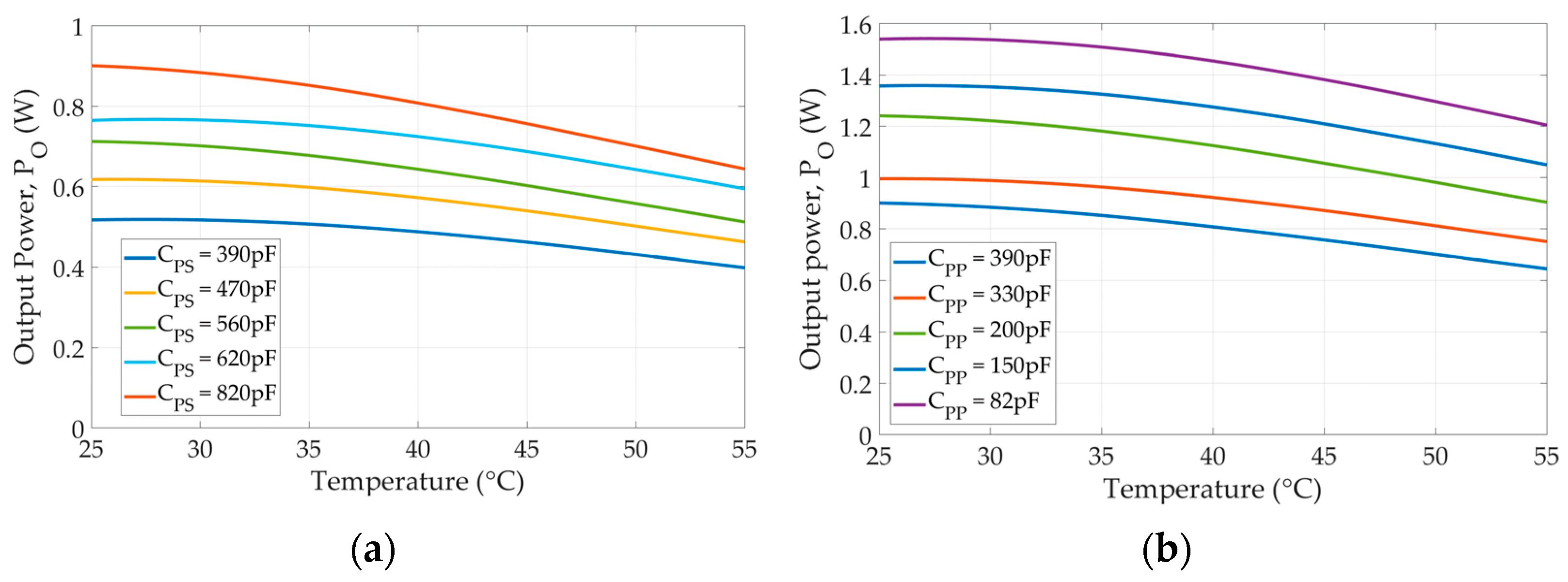
To increase the output power, we increased the series capacitance and decreased the parallel capacitance of the LCC resonant circuit, which raised the coil current and, in turn, increased the output power.
Figure 11a depicts the compensation of the output power by increasing the series capacitance and decreasing the parallel capacitance. The output power PO was raised to approximately 1 W by increasing the series capacitance from 390 pF to 820 pF. In order to increase the output power more, the parallel capacitance decreased from 390 pF to 82 pF. The change in the output power with the parallel capacitance is shown in Figure 11b.
In the original design, the series and parallel capacitances of the resonant circuit are all given as 390 pF. With increasing temperature, the equivalent and mutual inductances increased, resulting in a shift of the resonant frequency in the case of the fixed capacitances. However, the attached series resistor can extend the bandwidth but cannot adjust the resonant frequency. Therefore, to keep the resonant frequency within the allowable bandwidth, according to the variation in the equivalent and mutual inductances, one can change the capacitances to increase the output power and keep the resonant frequency within the allowable bandwidth.
From Equation (12), it can be seen that the relationship between the load current and the series capacitance is positively correlated. Moreover, the load current is also proportional to the output power as shown in Equation (10). Therefore, the series capacitance begins to be increased from the original of 390 pF; the output power gradually increases as the series capacitance increases, as shown in Figure 11a. However, a continuous increase in series capacitance would lead to an excessive shift in resonant frequency and exceed the allowable bandwidth. Therefore, the series capacitance is changed to 820 pF, while the parallel capacitance is reduced from the original value of 390 pF. As Figure 11b shows, the output power would increase with a decreasing parallel capacitance if the series capacitance is 820 pF. When the parallel capacitance is reduced to 82 pF, the output power can be increased to over 1.5 W at 25 °C as in the original.
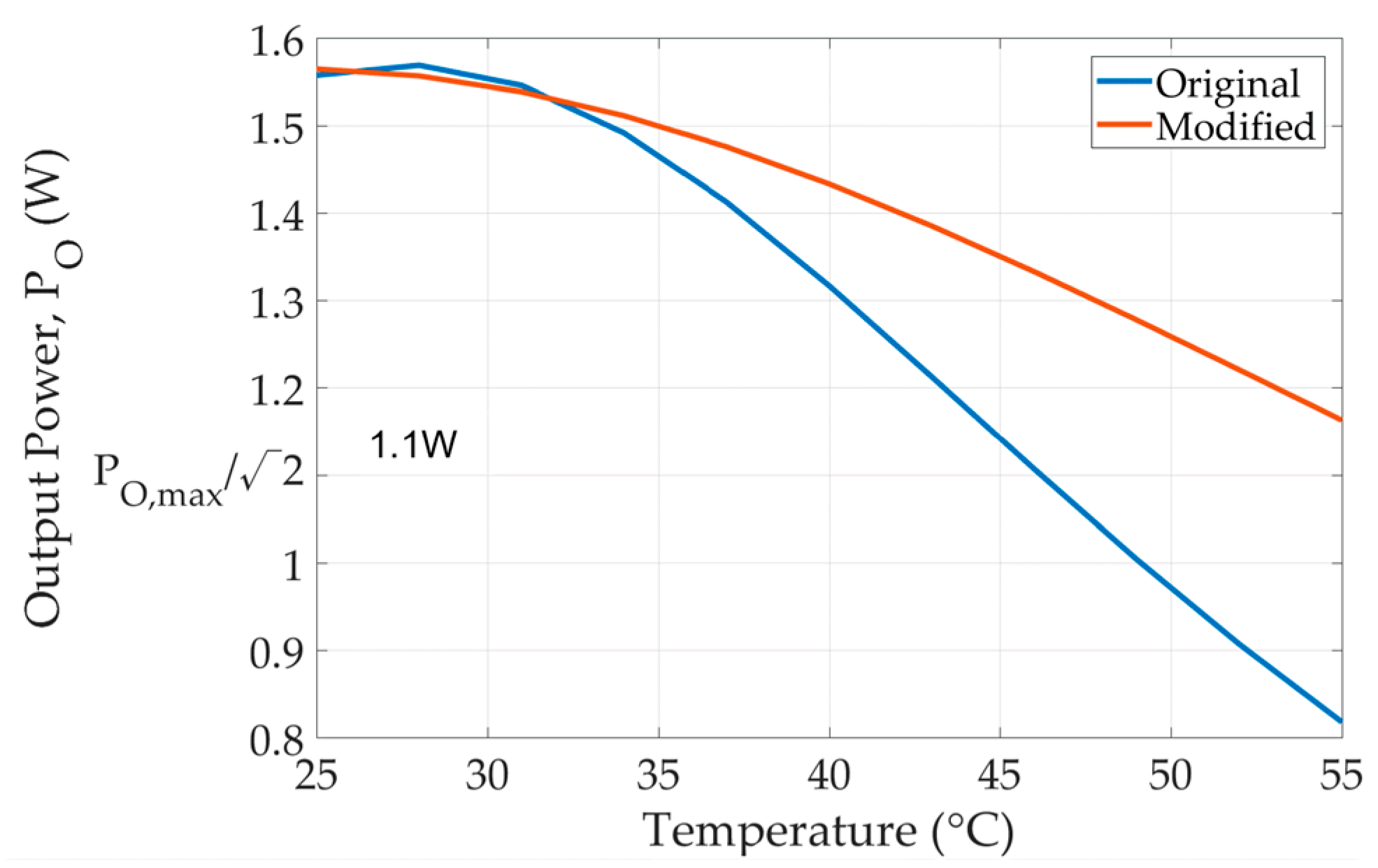
The modification of the LCC resonant circuit increased the output power PO at high temperatures. Figure 12 shows a comparison between the original design and the modified design. The output power of the modified system was 0.35 W higher than that of the original at 55 °C.
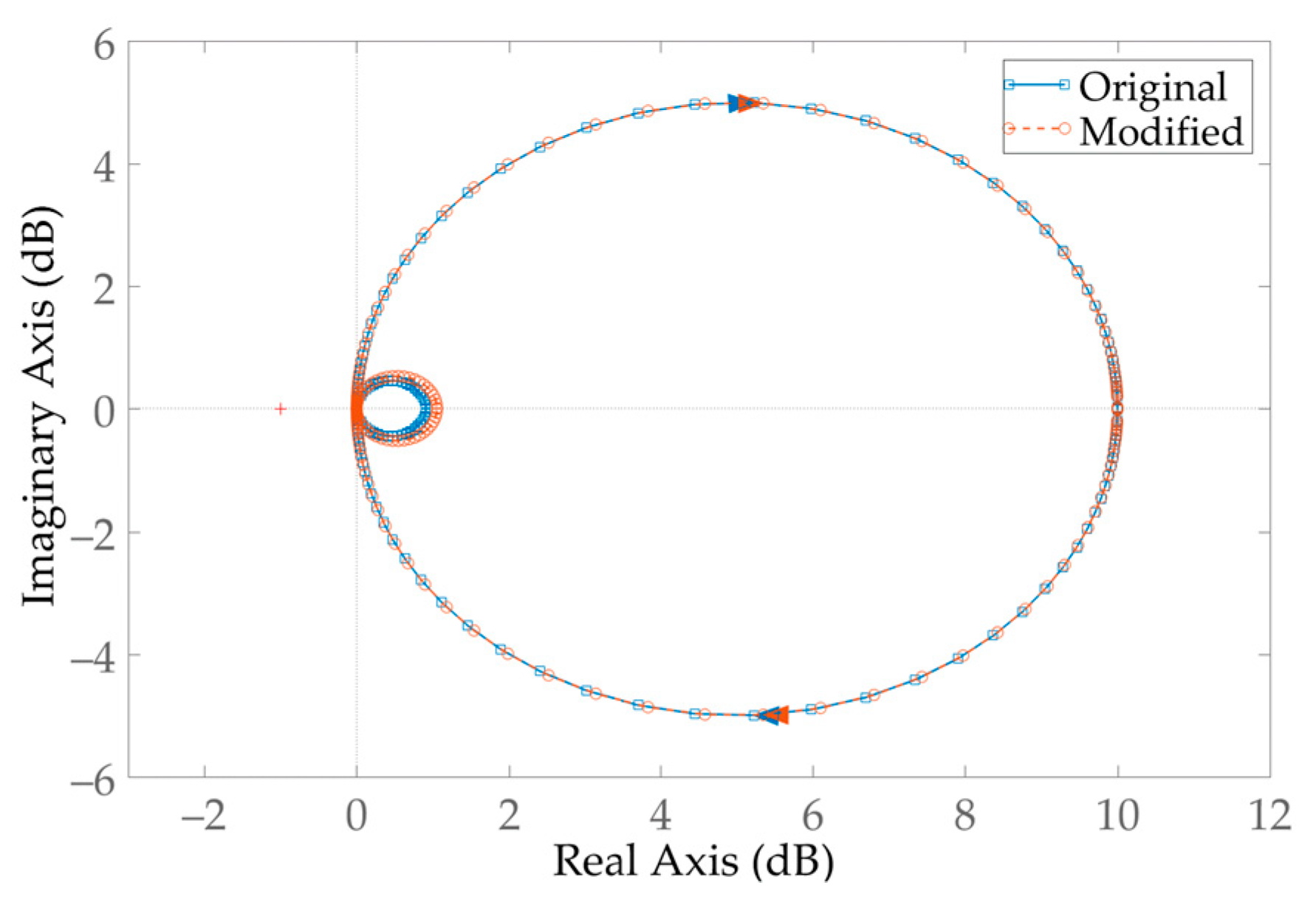
Comparing the stability between the original system and the system modified according to the Nyquist stability criterion, there are no significant differences, as depicted in Figure 13. The temperature rise was improved only by adjusting the compensation capacitance and adding a small series resistor, as shown by the transfer function; the structure of the transfer function could not theoretically be changed by the adjustment. This assumption is also confirmed by the Nyquist stability criterion in the simulation.
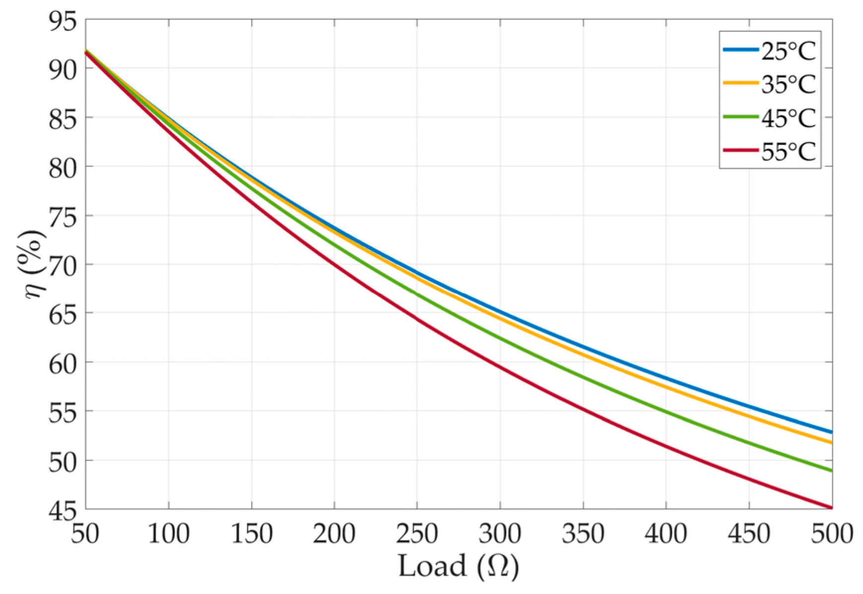
Figure 14 shows the relationships between the load and the system efficiency. In the figure, less load resistance has high efficiency; the efficiency decreases as the load resistance increases. According to the relationship between the current and the resistance, less resistance means the system load is heavy; on the contrary, more resistance indicates a light load. The result suggests that the proposed modification applies to the wireless power transfer system with a heavy load.
The bifurcation of the LCC-S resonant wireless power transfer system is analyzed according to the papers [19,20].
The bifurcation criterion is given as
The symbols QP and QS in the expression above represent the quality of the transmitter and receiver circuits. The quality factors are, respectively,
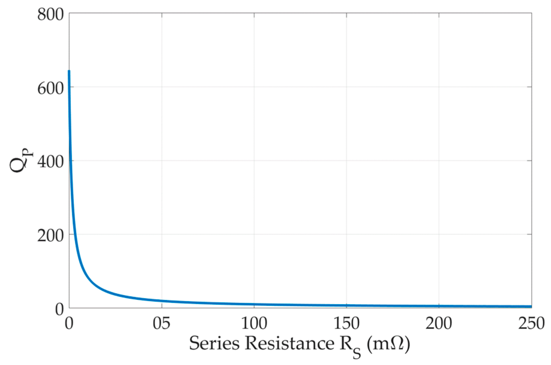
The QP and QS were calculated according to Table 1. The result is shown in Figure 15. The QP value will reduce substantially as the series resistance increases, but it is still more than the bifurcation criterion since the QS is considerably small. It can be seen that the system will not be out of the bifurcation-free range caused by the series resistance increase.
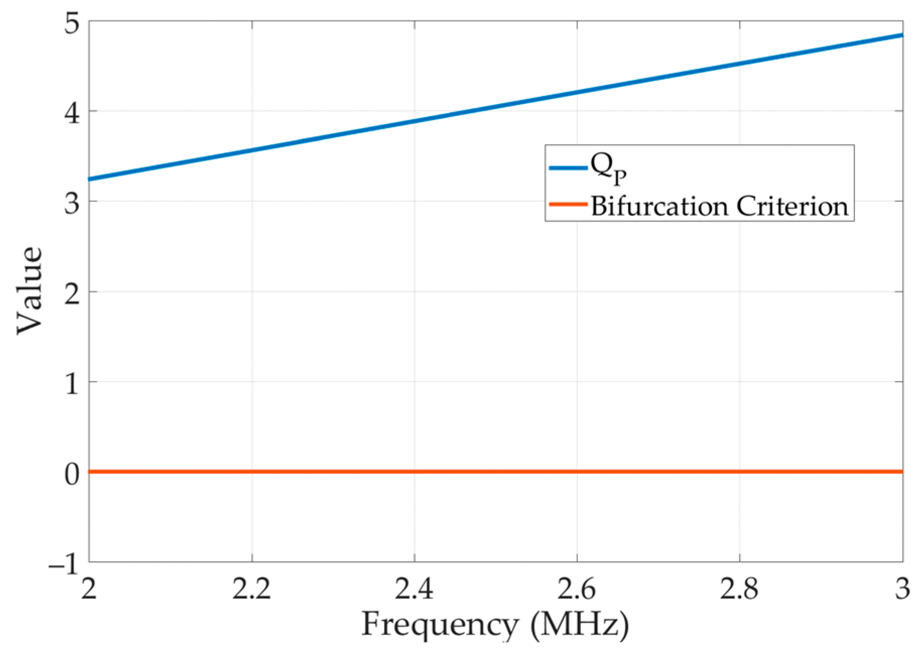
With adjustment of the compensation capacitances, the bifurcation criterion did not considerably vary, while the QP continued to rise; a comparison between QP and the bifurcation criterion is shown in Figure 16.
The QP is larger than the criterion regardless of whether the resistance is added or the compensation capacitance is adjusted. The analysis results suggested that the system will not produce a bifurcation phenomenon by the addition of the series resistance and adjustment of the capacitances.
4. Discussion
The simulation results revealed that the output power at high temperatures can be increased by increasing the series resistance and altering the capacitance values. Increasing the series resistance increased the bandwidth to cover the new circuit resonance frequency caused by the increase in the self-inductance. Although the bandwidth covered the new resonance frequency, the output power was far less than the original output power. By adjusting the capacitance, the output power was further increased.
As already stated in the Introduction Section, adding a core to the coupling coil enhances transmission efficiency. However, the output power decreases at high temperatures. The wireless power transfer technology is employed in several applications and at different temperatures; hence, considering the effect of the operating ambient temperature is essential. Based on the simulation results presented herein, future studies can focus on the frequency of drive source design for the LCC-S-compensated topology.
5. Conclusions
At high temperatures, the core added to the coupling coil to enhance the transmission efficiency of the wireless power transfer system results in a decrease in the power being supplied to the load, because the temperature coefficient of the core material renders the power output unevenly. For a given frequency of the drive source, a narrow bandwidth results in decreasing output power with increasing temperature. Employing appropriate system component values can help mitigate this problem, rendering the output power level to be more than the half-power.
Author Contributions
Conceptualization, C.-L.C.; methodology, C.-L.C.; resources, C.-W.H.; writing—original draft preparation, C.-L.C.; writing—review and editing, C.-W.H. All authors have read and agreed to the published version of the manuscript.
Funding
This work was supported in part by the Ministry of Science and Technology, Taiwan, under contracts MOST-109-2622-E-224 -011-, 110-2221-E-150 -041- and IRIS “Intelligent Recognition Industry Service Research Center” from The Featured Areas Research Center Program within the framework of the Higher Education Sprout Project by the Ministry of Education (MOE) in Taiwan.
Conflicts of Interest
The authors declare no conflict of interest.
References
- Mohammad, M.; Choi, S. Optimization of Ferrite Core to Reduce the Core Loss in Double-D Pad of Wireless Charging System for Electric Vehicles. In Proceedings of the 2018 IEEE Applied Power Electronics Conference and Exposition (APEC), San Antonio, TX, USA, 4–8 March 2018; pp. 1350–1356. [Google Scholar]
- Chen, K.; Pan, J.; Yang, Y.; Cheng, K.W.E. Optimization of ferrites structure by using a new core-less design algorithm for electric vehicle wireless power transfer. Energies 2021, 14, 2590. [Google Scholar] [CrossRef]
- Lee, J.J.; Hong, Y.K.; Bae, S.; Park, J.H.; Jalli, J.; Abo, G.S.; Syslo, R.; Choi, B.C.; Donohoe, G.W. High-quality factor Ni-Zn ferrite planar inductor. IEEE Trans. Magn. 2010, 46, 2417–2420. [Google Scholar] [CrossRef]
- Goldman, A. Modern Ferrite Technology; Springer Science & Business Media: New York, NY, USA, 2006. [Google Scholar]
- Gaona, D.E.; Long, T. Design Considerations for High-Power-Density IPT Pads Using Nanocrystalline Ribbon Cores. In Proceedings of the 2020 IEEE PELS Workshop on Emerging Technologies: Wireless Power Transfer (WoW), Seoul, Korea, 5–9 May 2020; pp. 377–382. [Google Scholar]
- Chwei-Sen, W.; Stielau, O.H.; Covic, G.A. Design considerations for a contactless electric vehicle battery charger. IEEE Trans. Ind. Electron. 2005, 52, 1308–1314. [Google Scholar] [CrossRef]
- Cirimele, V.; Rosu, S.G.; Guglielmi, P.; Freschi, F. Performance evaluation of wireless power transfer systems for electric vehicles using the opposition method. In Proceedings of the 2015 IEEE 1st International Forum on Research and Technologies for Society and Industry Leveraging a Better Tomorrow (RTSI), Turin, Italy, 16–18 September 2015; pp. 546–550. [Google Scholar]
- Lu, F.; Zhang, H.; Mi, C. A review on the recent development of capacitive wireless power transfer technology. Energies 2017, 10, 1752. [Google Scholar] [CrossRef] [Green Version]
- Ali, N.; Liu, Z.; Armghan, H.; Ahmad, I.; Hou, Y. LCC-S-based integral terminal sliding mode controller for a hybrid energy storage system using a wireless power system. Energies 2021, 14, 1693. [Google Scholar] [CrossRef]
- Yang, S.; Deng, X.; Lu, J.; Wu, Z.; Du, K. Light-load efficiency optimization for an LCC-parallel compensated inductive power transfer battery charger. Electronics 2020, 92, 2080. [Google Scholar] [CrossRef]
- Shevchenko, V.; Husev, O.; Strzelecki, R.; Pakhaliuk, B.; Poliakov, N.; Strzelecka, N. Compensation topologies in IPT Systems: Standards, requirements, classification, analysis, comparison and application. IEEE Access 2019, 7, 120559–120580. [Google Scholar] [CrossRef]
- Yang, K. Resonant Circuit Generates a High Frequency Magnetic Field Using This Resonant Technique. Available online: https://www.electronicdesign.com/technologies/analog/article/21806675/generate-a-highfrequency-magnetic-field-using-this-resonant-technique (accessed on 28 June 2018).
- Kim, J.; Wei, G.; Kim, M.; Jong, J.; Zhu, C. A comprehensive study on composite resonant circuit-based wireless power transfer systems. IEEE Trans. Ind. Electron. 2018, 65, 4670–4680. [Google Scholar] [CrossRef]
- Imura, T.; Okabe, H.; Hori, Y. Basic experimental study on helical antennas of wireless power transfer for Electric Vehicles by using magnetic resonant couplings. In Proceedings of the 2009 IEEE Vehicle Power and Propulsion Conference, Dearborn, MI, USA, 7–10 September 2009; pp. 936–940. [Google Scholar]
- Tishechkin, S.; Ben-Yaakov, S. Adaptive Capacitance Impedance Matching (ACIM) of WPT Systems by Voltage Controlled Capacitors. In Proceedings of the 2019 IEEE PELS Workshop on Emerging Technologies: Wireless Power Transfer (WoW), London, UK, 18–21 June 2019; pp. 396–400. [Google Scholar]
- Beams, D.M.; Annam, S.G. Validation of a Reflected-Impedance Design Method for Wireless Power Transfer Applications. In Proceedings of the 2012 IEEE 55th International Midwest Symposium on Circuits and Systems (MWSCAS), Boise, ID, USA, 5–8 August 2012; pp. 758–761. [Google Scholar]
- Steigerwald, R.L. A comparison of half-bridge resonant converter topologies. IEEE Trans. Power Electron. 1988, 3, 174–182. [Google Scholar] [CrossRef]
- Kim, J.; Wei, G.; Zhu, C.; Rim, C. Quality Factor and Topology Analysis of the Series-Parallel Combined Resonant Circuit-Based Wireless Power Transfer System. In Proceedings of the 2017 IEEE Transportation Electrification Conference and Expo, Asia-Pacific (ITEC Asia-Pacific), Harbin, China, 7–10 August 2017; pp. 1–5. [Google Scholar]
- Wang, C.-S.; Covic, G.A.; Stielau, O.H. Power transfer capability and bifurcation phenomena of loosely coupled inductive power transfer systems. IEEE Trans. Ind. Electron. 2004, 51, 148–157. [Google Scholar] [CrossRef]
- Fernandes, R.C.; de Oliveira, A.A. Theoretical bifurcation boundaries for Wireless Power Transfer converters. In Proceedings of the 2015 IEEE 13th Brazilian Power Electronics Conference and 1st Southern Power Electronics Conference (COBEP/SPEC), Fortaleza, Brazil, 29 November–2 December 2015; pp. 1–4. [Google Scholar]
Figure 1.
LCC-S-compensated topology for wireless power transfer systems.

Figure 2.
Variation in the output power with respect to temperature.

Figure 3.
The illustration of the output power variation in different frequencies.

Figure 4.
Variation in bandwidth and output power with respect to series resistance.

Figure 5.
The variation in the output power per the driving voltage increases in different temperatures.
Figure 5.
The variation in the output power per the driving voltage increases in different temperatures.

Figure 6.
The variation in the output power per load in different temperatures.

Figure 7.
(a) The variation in the output power when the load RL = 300 Ω in different temperatures, and (b) the input power variation in the case of the driving voltage increment for fixed load in RL = 300 Ω.
Figure 7.
(a) The variation in the output power when the load RL = 300 Ω in different temperatures, and (b) the input power variation in the case of the driving voltage increment for fixed load in RL = 300 Ω.

Figure 8.
The variation in the output power for increasing the number of turns for the coupling coils.
Figure 8.
The variation in the output power for increasing the number of turns for the coupling coils.

Figure 9.
(a) Bandwidth and (b) output power for different series resistance values.

Figure 10.
Variation in (a) output power and (b) input power with respect to series resistance.

Figure 11.
(a) Increasing the series capacitance to elevate PO to approximately 1 W and (b) decreasing the parallel capacitance to increase PO.
Figure 11.
(a) Increasing the series capacitance to elevate PO to approximately 1 W and (b) decreasing the parallel capacitance to increase PO.

Figure 12.
Comparison of the output power PO in the original circuit and that in the circuit modified by adding series resistance and adjusting capacitance in the LCC resonant circuit.
Figure 12.
Comparison of the output power PO in the original circuit and that in the circuit modified by adding series resistance and adjusting capacitance in the LCC resonant circuit.

Figure 13.
A Nyquist stability comparison between the original and modified designs.

Figure 14.
The variation in the efficiencies in different loads at different temperatures.

Figure 15.
The quality factor on the transmitter circuit, QP, corresponds to the series resistance increment.
Figure 15.
The quality factor on the transmitter circuit, QP, corresponds to the series resistance increment.

Figure 16.
The comparison of the QP and bifurcation criterion.


Table 1.
Parameters of LCC-S-based wireless power transfer system.
| Parameter | Symbol | Value |
|---|---|---|
| Tx coupling coil equivalent self-inductance | LP | 4.6 μH |
| Rx coupling coil equivalent self-inductance | LS | 4.6 μH |
| Core permeability from 25 °C to 55 °C | µ | 6000–6050 H/m |
| Coupling coefficient | k | 0.2 |
| Tx series compensation capacitance | CPS | 390 pF |
| Tx parallel compensation capacitance | CPP | 390 pF |
| Rx series compensation capacitance | CSS | 780 pF |
| Series resistance on the Tx | RS | 0–500 mΩ |
| Load resistance | RL | 500 Ω |
| Driving voltage | VS | 5 Vp-p |
| Frequency of the drive source | fS | 2.65 MHz |
Publisher’s Note: MDPI stays neutral with regard to jurisdictional claims in published maps and institutional affiliations. |
© 2021 by the authors. Licensee MDPI, Basel, Switzerland. This article is an open access article distributed under the terms and conditions of the Creative Commons Attribution (CC BY) license (https://creativecommons.org/licenses/by/4.0/).
Share and Cite
MDPI and ACS Style
Chen, C.-L.; Hung, C.-W. Improving LCC Series-Based Wireless Power Transfer System Output Power at High Temperature. Electronics 2021, 10, 2875. https://0-doi-org.brum.beds.ac.uk/10.3390/electronics10222875
AMA Style
Chen C-L, Hung C-W. Improving LCC Series-Based Wireless Power Transfer System Output Power at High Temperature. Electronics. 2021; 10(22):2875. https://0-doi-org.brum.beds.ac.uk/10.3390/electronics10222875
Chicago/Turabian StyleChen, Chien-Lung, and Chung-Wen Hung. 2021. "Improving LCC Series-Based Wireless Power Transfer System Output Power at High Temperature" Electronics 10, no. 22: 2875. https://0-doi-org.brum.beds.ac.uk/10.3390/electronics10222875
Note that from the first issue of 2016, this journal uses article numbers instead of page numbers. See further details here.