1. Introduction
Compared to traditional plug-in systems, inductive wireless energy transmission systems have advantages such as flexibility, convenience, electrical isolation, and strong environmental adaptability [
1]. It has been employed in many applications. For example, in the field of electric vehicles, the inductive power transfer (IPT) method has a greater advantage for the electric vehicle (EV) battery charger due to its convenience and safety as compared to the plugged-in charger [
2]. In the area of implantable medical devices, compared to batteries, IPT can theoretically achieve an unlimited lifetime through wireless power transfer, without the need for surgery to replace the battery, greatly reducing the patient’s pain [
3]. In the field of consumer electronics, inductively coupled chargers are becoming more and more popular in wireless charging of mobile phones, laptops, and other handheld devices as proposed in [
4].
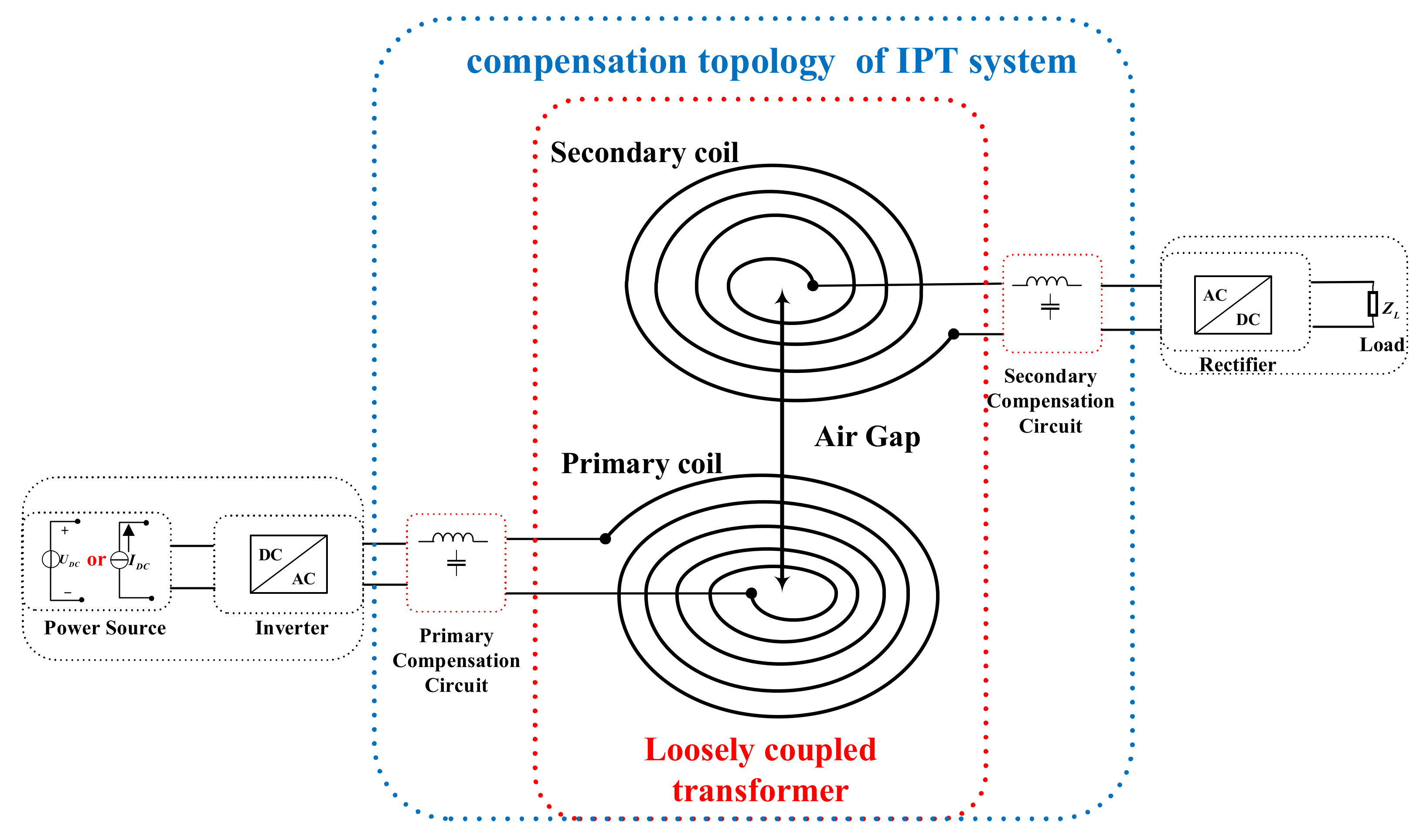
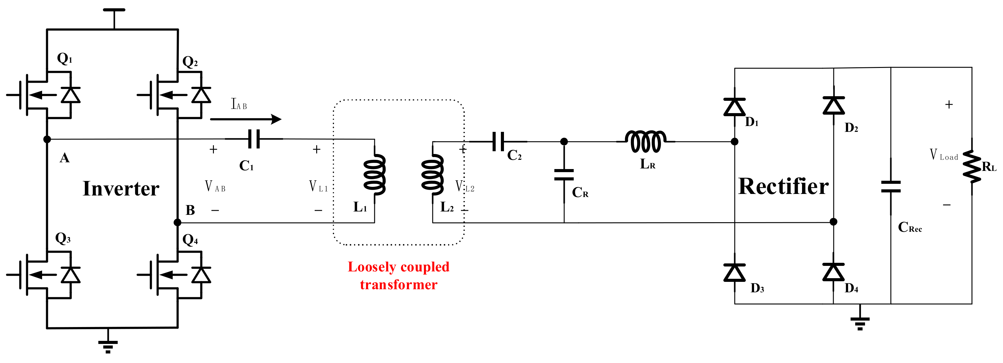
Figure 1 illustrates the schematic diagram of an IPT system. At the primary side, the IPT system is powered by a DC source U
DC (I
DC), and the inverter produces a constant AC voltage or current. At the secondary side, a rectifier is applied to generate a DC voltage to the load Z
L. As shown in
Figure 1, in order to transfer power within a certain distance in the IPT system, a loosely coupled transformer (LCT) that involves the primary coil and the secondary coil must be used. Due to the existence of the air gap between the coils, when the distance of the coils increases, the coupling coefficient between the coils becomes smaller while leakage inductance becomes bigger. Uncoupled magnetic flux generates significant reactive power, which increases the ratings of the drive circuit and reduces the power transfer capability [
5]. Therefore, compensation circuits are generally required to achieve or improve the following characteristics:
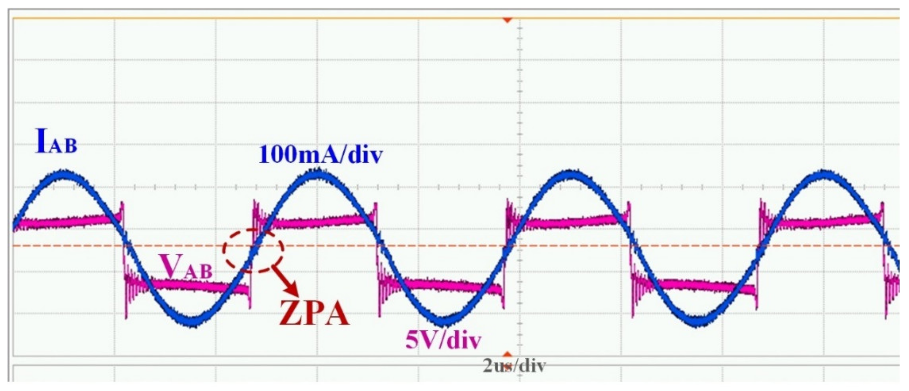
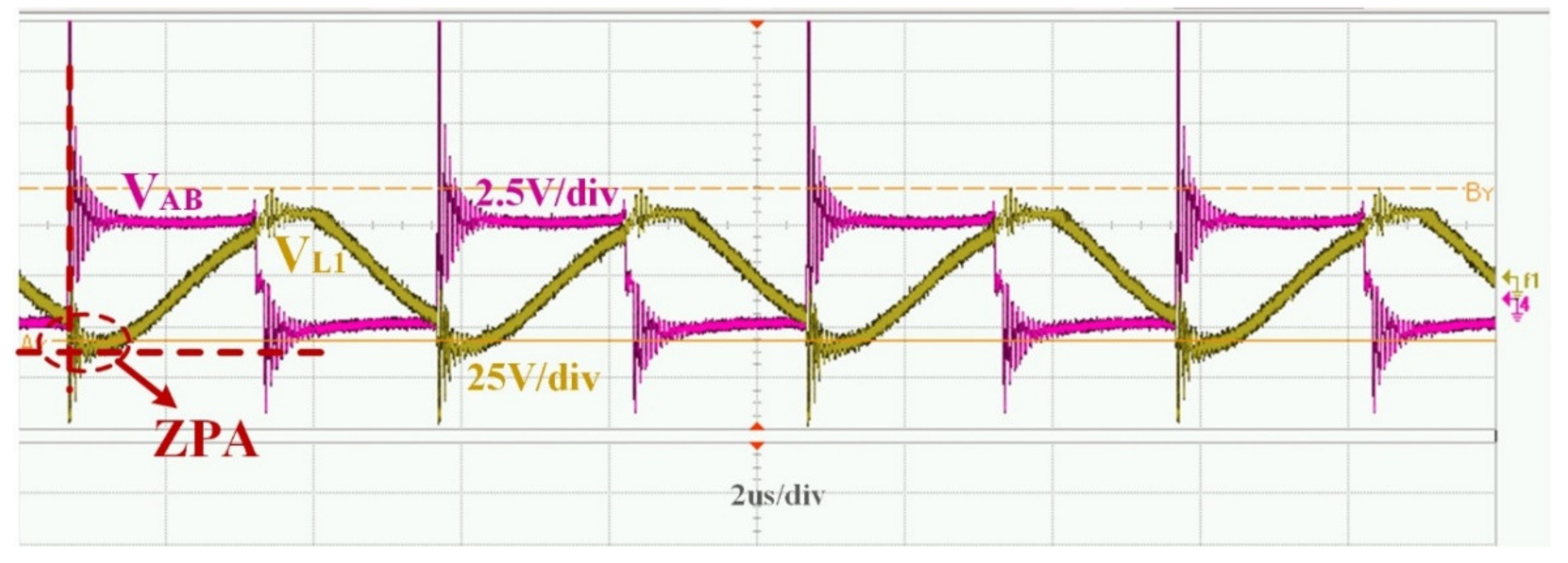
Implementing the zero-phase angle (ZPA) feature. In order to achieve near-zero reactive power and transfer more power to the load, it is desirable for the IPT system to operate at the zero-phase-angle frequency [
6]. At this frequency, the equivalent impedance seen by the source is a pure resistance, minimizing the volt-ampere (VA) ratings of the power supply and maximizing the transfer capability.
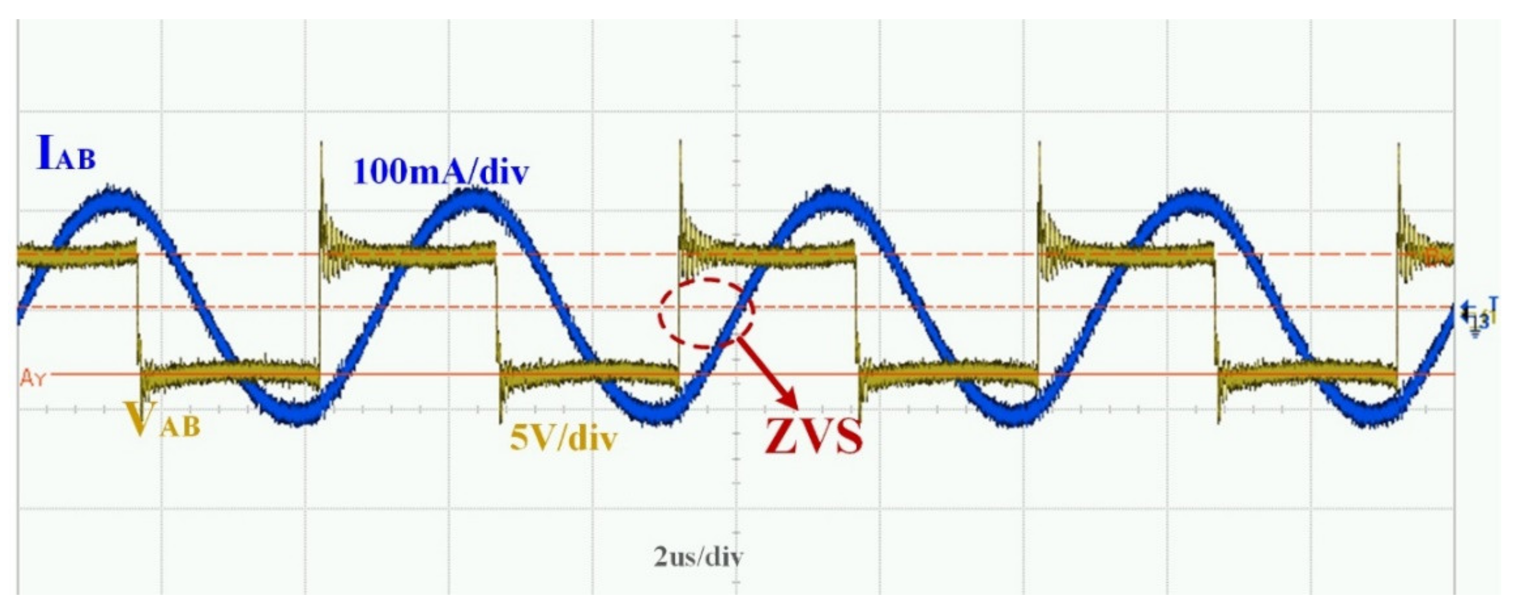
Facilitating zero-voltage switching (ZVS) and improving system efficiency. Hard switching refers to the phenomenon that the current and voltage on the power switch overlap in a large area during the turn-on process of the power switch. This is the main contributor to energy loss. Especially when the switching frequency is high, the conversion rate of the power supply in the hard-switching state decreases, the switching loss and the stress it bears also increases exponentially, which greatly reduces the switching efficiency. The zero-voltage switching is to turn MOS on when the voltage crosses zero, which requires the circuit to be slightly inductive when the current crosses zero, thus causing resonant-tank current to lag the voltage. In this way, the overlap area of voltage and current during turn-on is reduced, thereby reducing loss and obtaining higher efficiency. It is worth noting that based on the realization of near-zero reactive power, only a small adjustment of the compensation parameters can make the circuit appear slightly inductive to facilitate ZVS [
5]. Therefore, it is critical to design the parameters of the compensation circuit properly to realize the characteristics of ZPA.
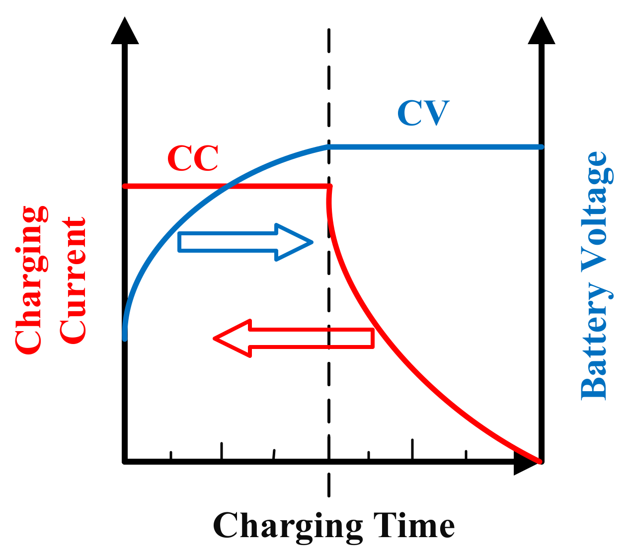
Load-independent constant-voltage (CV) or constant-current (CC) output. In wireless power transmission systems, load-independent CV or CC output is necessary in many cases. In recent years, lithium-ion batteries are increasingly used in EVs [
7,
8]. To ensure the safety of the lithium-ion battery and the effectiveness of the charging system, proper charging strategies are crucial [
9]. Constant-current–constant-voltage charging is often adopted due to efficiency and safety. The typical charging process of an EV lithium-ion battery is shown in
Figure 2 [
10]. It can be seen from
Figure 2 that the charging process is divided into two stages. The first stage is a constant current process, with the charging current basically unchanged and the battery voltage rising rapidly. The second stage is a constant-voltage process. When the battery voltage reaches the specified level, the charger enters the CV charging process, where the battery voltage remains basically unchanged and the charging current gradually decreases until it approaches zero. In addition, in order to ensure the safe operation of the implantable devices, the output voltage must remain basically unchanged within a large range of load changes [
11]. Designing the compensation topology meticulously can be a better alternative compared to utilizing a backend DC–DC converter or frequency control, which makes the control circuits simplified to obtain better system stability and reduce energy loss to improve system efficiency.
Freeing from LCT parameters to get higher design freedom. Low design freedom means that the input-to-output transfer function is dependent on LCT parameters, which implies the fact that once the input voltage or current is predetermined, the output voltage or current does not change unless a new LCT with different parameters is used [
12]. However, the redesign of the LCT is time-consuming and complex. In consequence, designing the compensation topology with the input-to-output transfer function independent of LCT parameters is of great importance.
Less use of compensation components. The authors of [
13] proposed a compensation topology, named double-side LCC compensation topology, which poses all the above mentioned characteristics including ZPA, ZVS, load-independent output current, and source-to-load transfer function independent of LCT parameters. However, it has six compensation elements, including one inductor and two capacitors at both the primary and secondary sides, which results in higher cost, more space, and a lower power density. Therefore, the use of fewer compensation elements while satisfying other characteristics mentioned above is also significant.
Some researchers have analyzed and designed how to realize the required characteristics for the compensation topology of an IPT system. Based on the traditional mutual inductance model of the LCT, the literature [
14] adopted the method of the separation of parameters to obtain the conditions of CV or CC. However, this approach of solving the equations derived from circuits can be tedious and time consuming. Moreover, the research has not made a comprehensive and systematic analysis of the ZPA characteristics of topology. Reference [
15] shows that by correctly combining resonant blocks with CC/CV output functions, compensation structures can achieve a constant output and a minimum input VA rating simultaneously. However, for some topologies, the method of separating parameters is still used to obtain the compensation parameters of CC or CV, and the given model cannot intuitively reach the conditions of realizing ZPA. The literature [
16] proposes a general modeling method based on the basic LC network, T-network, and π-network for realizing load-independent current and voltage output for compensation networks. However, this method is not straightforward and does not analyze the ZPA characteristic. In reference [
17], the compensation topologies are modeled as basic L-Section matching networks and the regularization mathematical expressions of load-independent current or voltage and the realization conditions of ZPA are given. However, it is not straightforward to solve the mathematical model of the circuit to obtain the conditions for constant output and pure input resistance. A graphical approach method [
18] based on gyrator is proposed to visually and systematically analyze the CC/CV output with ZPA operation of compensation topologies. However, CC/CV output and ZPA conditions cannot be obtained simultaneously by intuitive analysis.
Therefore, there are three common deficiencies in the above researches.
The modeling method is not intuitive. The compensation circuits are analyzed in the above literature mainly by mathematical methods. By solving the equation derived from the circuit or matrix manipulation, the characteristics of the compensation circuit are obtained, although the equation approach may be universal and unified. However, it is usually tedious and time consuming;
In addition, all the above researches use new models or adopt a new perspective to analyze the existing compensation circuits, some of the literature focuses on how to design a new compensation topology with higher design freedom and fewer compensating components;
The polarity of induced voltage is ignored. Under different resonant conditions, the voltage waveform of the secondary coil and that of the primary coil may be in-phase or antiphase. This causes the equivalent model to have two symbols and frequency bifurcation phenomena.
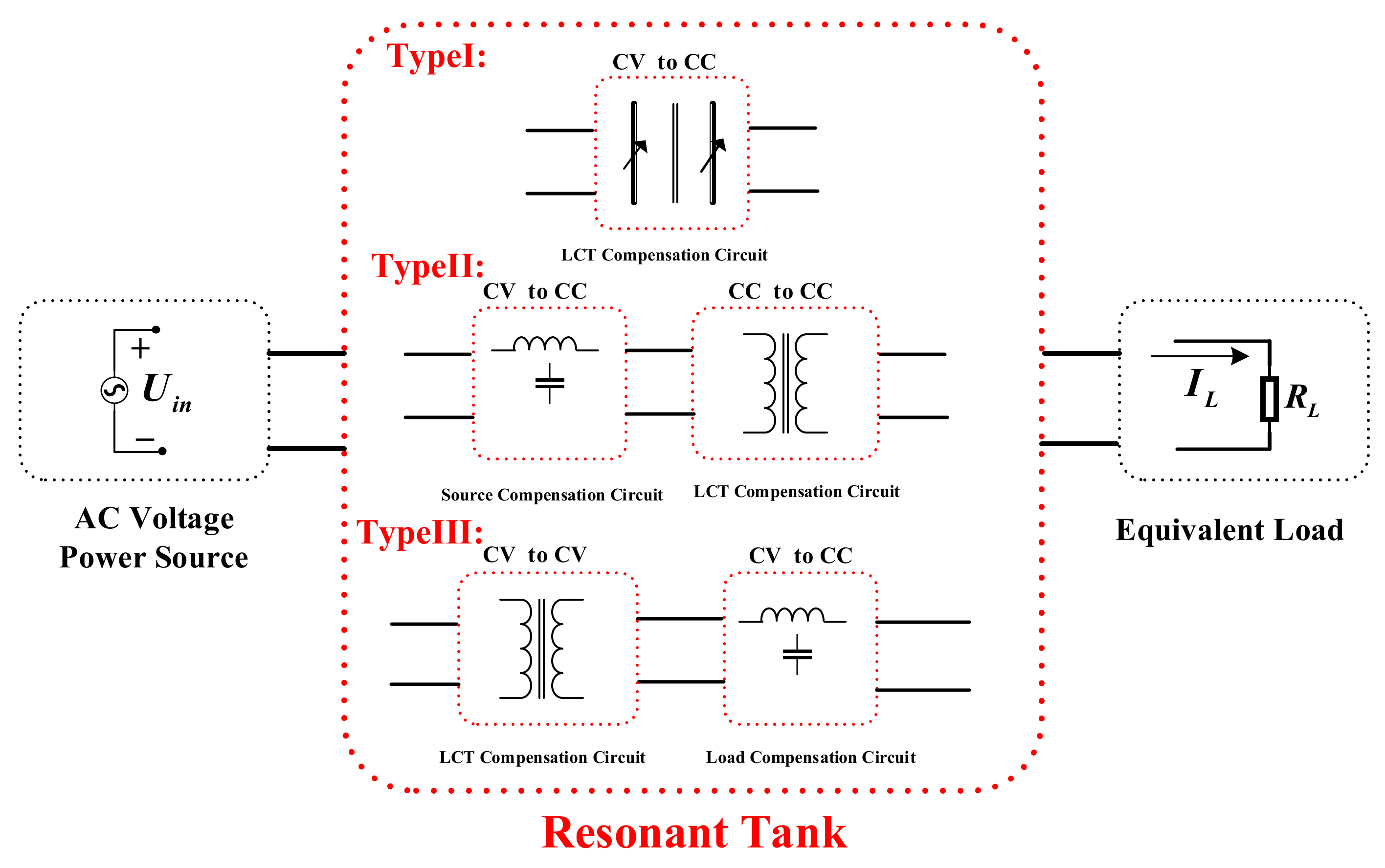
As a supplement and improvement of previous design methods, a graphical and simple design methodology is proposed in this paper. The ideal transformer and ideal gyrator are adopted to establish four types of models for LCT: CV input to CV output, CV input to CC output, CC input to CV output, and CC input to CC output. Two models of voltage-current conversion at the source and load side are also constructed. The combination of four types of LCT models with the source-side/load-side conversion models can realize the load-independent CV or CC output from voltage/current source to load. Based on the above design methodology, 12 novel compensation topologies fed by a voltage source are stated. They all provide the characteristics of ZPA, easy achievement of ZVS, load-independent CV or CC output, and LCT-unconstrained transfer function. The conditions of these characteristics can be obtained only by simply observing the equivalent model given by the design method in this paper, giving a new perspective being free from the constraints of complex equations. Moreover, compared to compensation topologies with less than three compensation elements, including S/S compensation topology, S/PS compensation topology, S/P compensation topology, and S/SP compensation topology, our topologies have source-to-load transfer functions independent of LCT parameters, which makes it possible to change the output power without replacing the LCT. Compared to double-sided LCC compensation topology, they all have fewer compensation components, which means lower cost, less space, and higher power density. In order to further verify theoretical analysis, a new prototype of S/LCC topology is constructed. The experimental results match well with the theory, validating the rightness of the newly proposed design method.
The remainder of this paper is structured as follows:
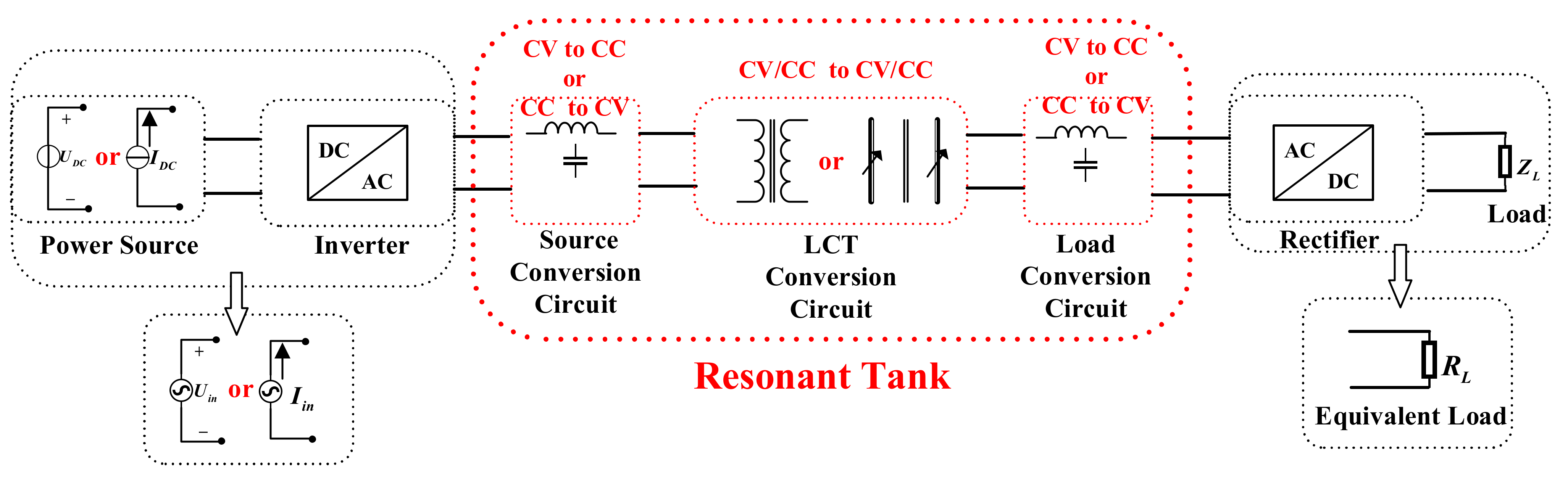
Section 2 gives the overall design block diagram of the IPT system to achieve load-independent voltage and current output.
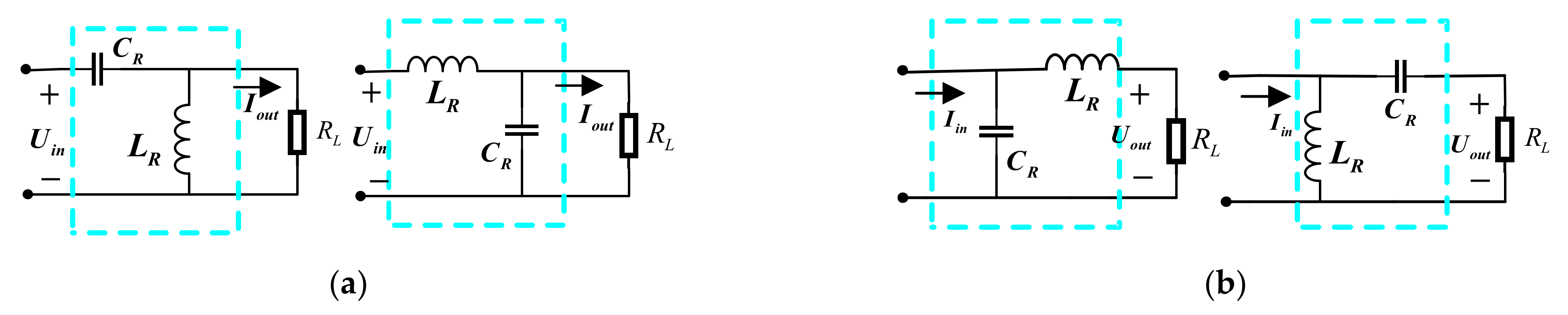
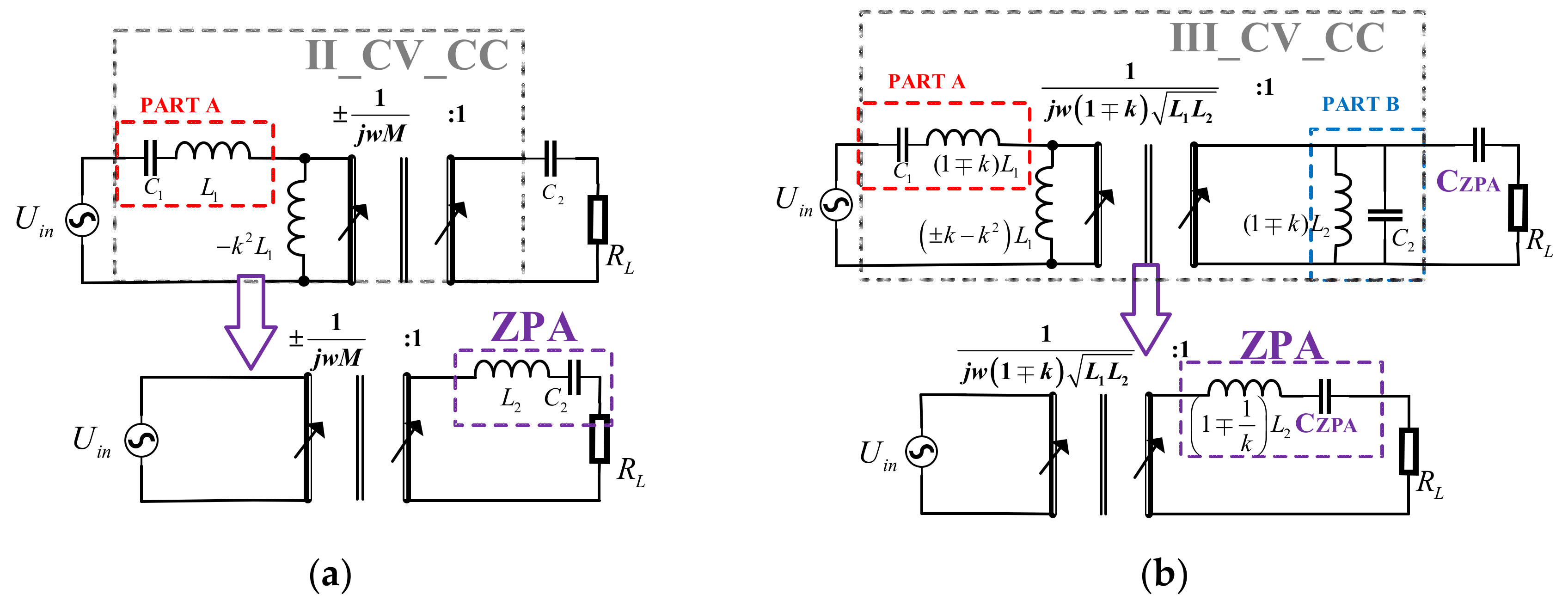
Section 3 discusses four types of models of LCT that utilize the ideal transformer and ideal gyrator for realizing conversion from CV/CC input to CV/CC output.
Section 4 presents two models of voltage and current conversion at the source and load side.
Section 5 analyzes the detailed design methodology for designing compensation circuits to realize load-independent CV or CC output at ZPA frequencies.
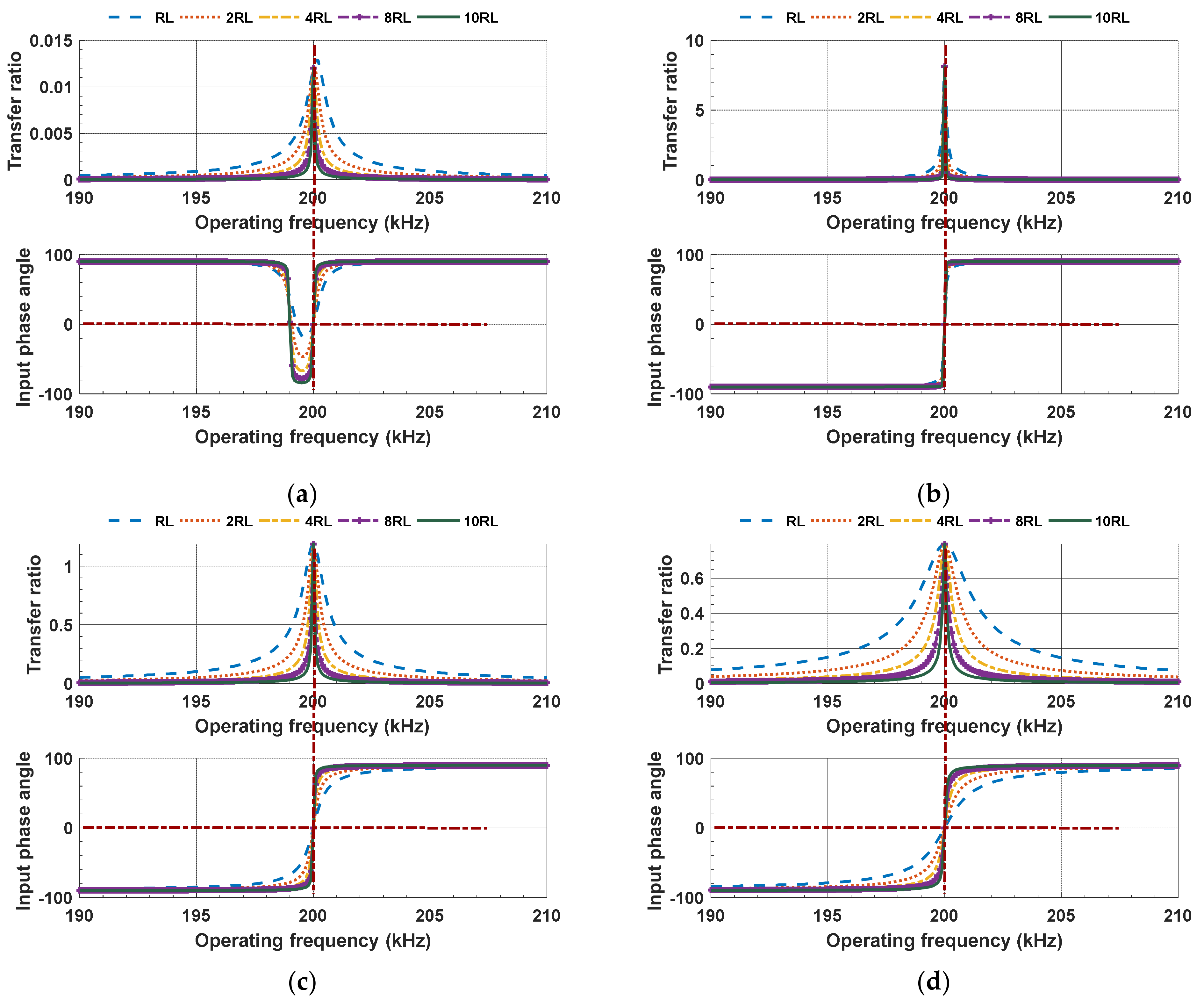
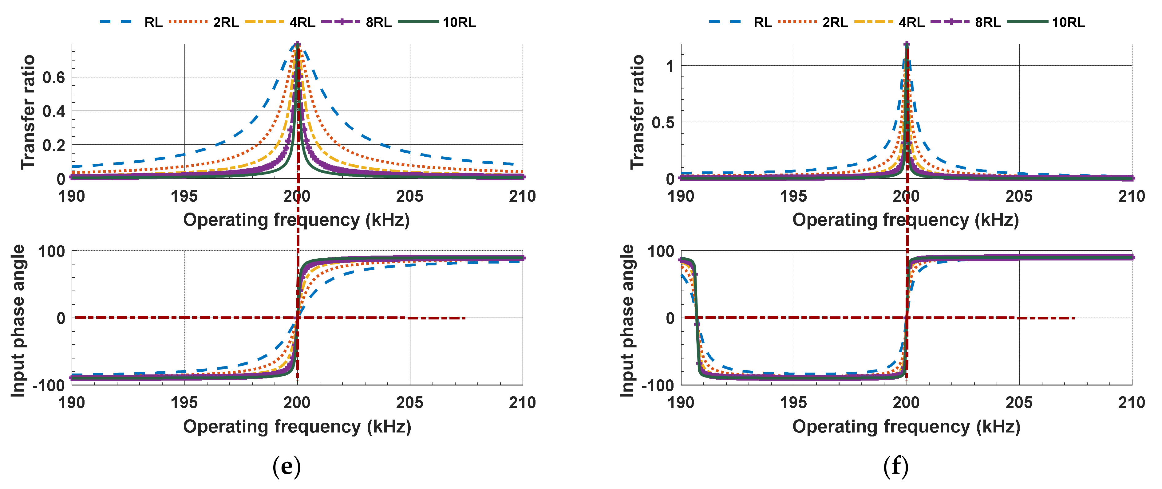
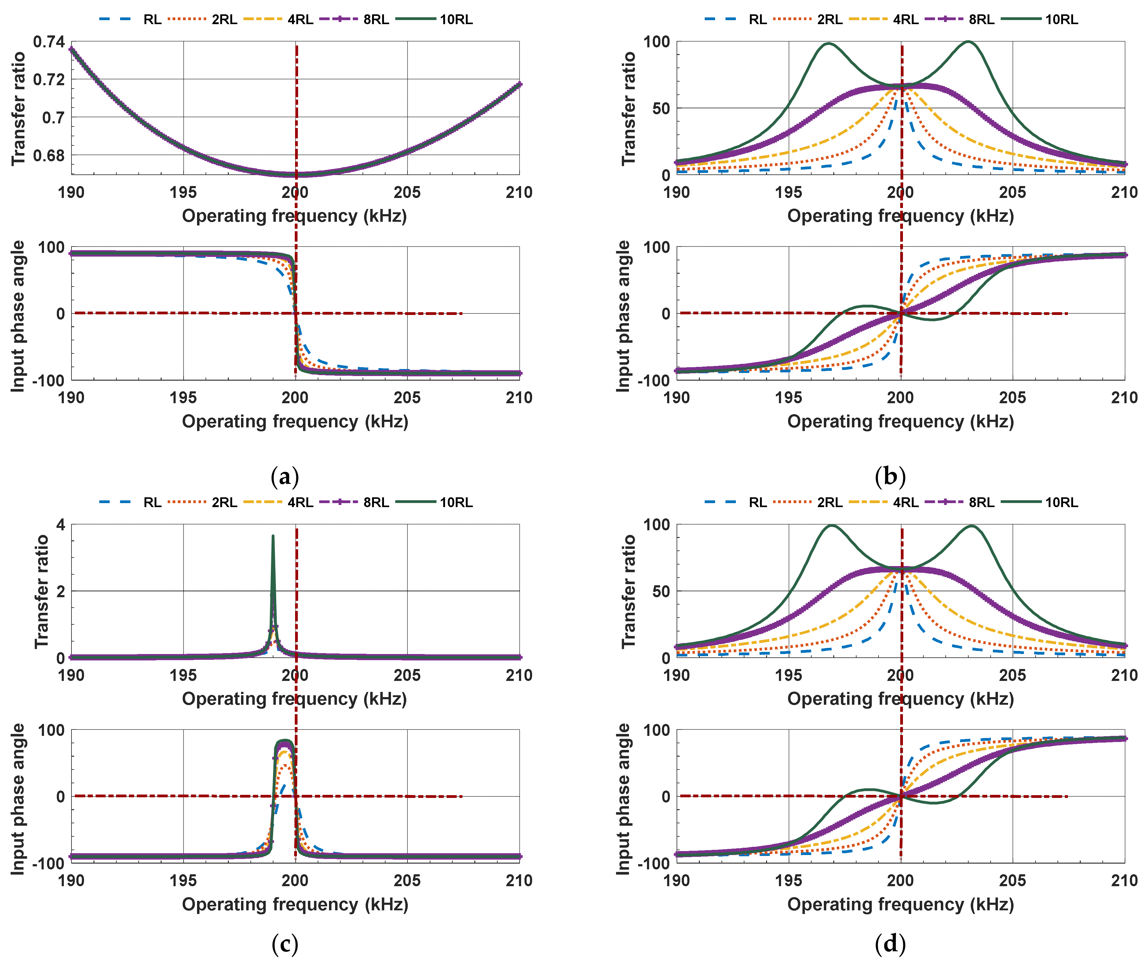
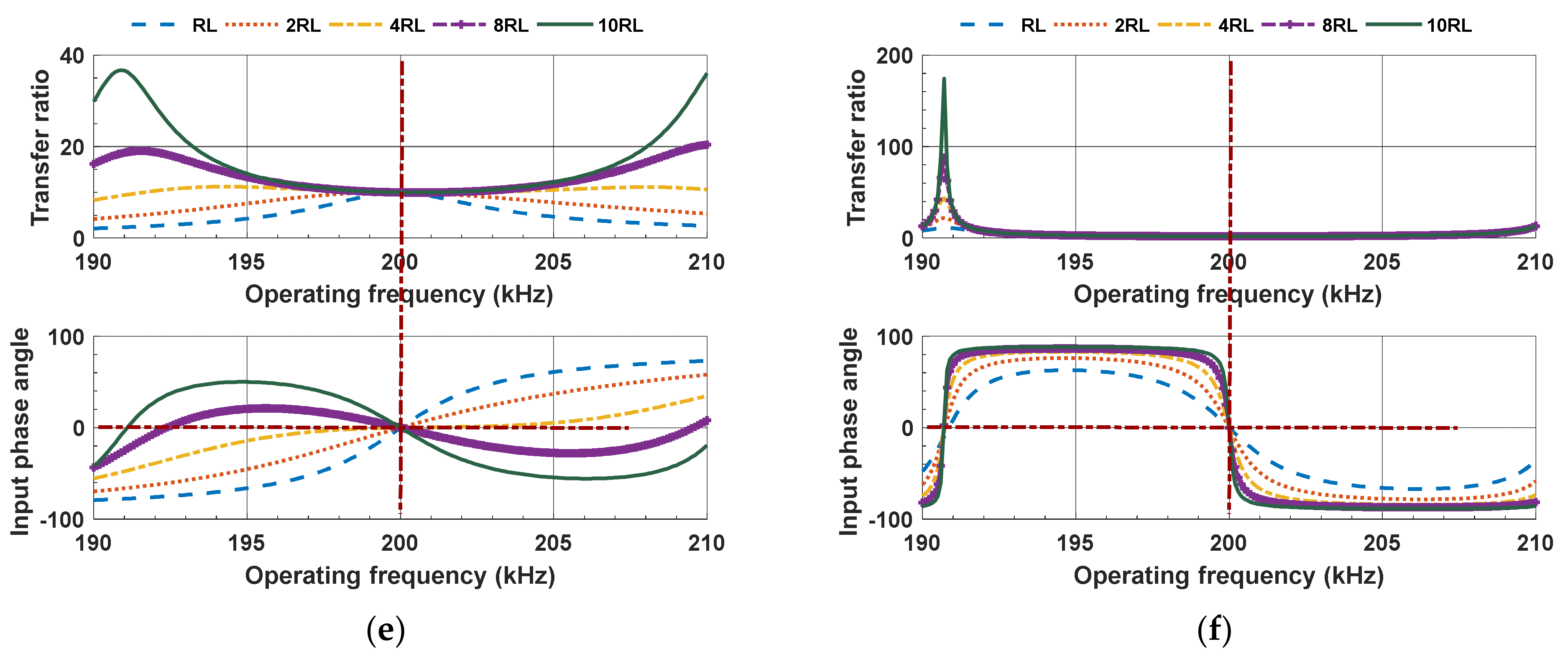
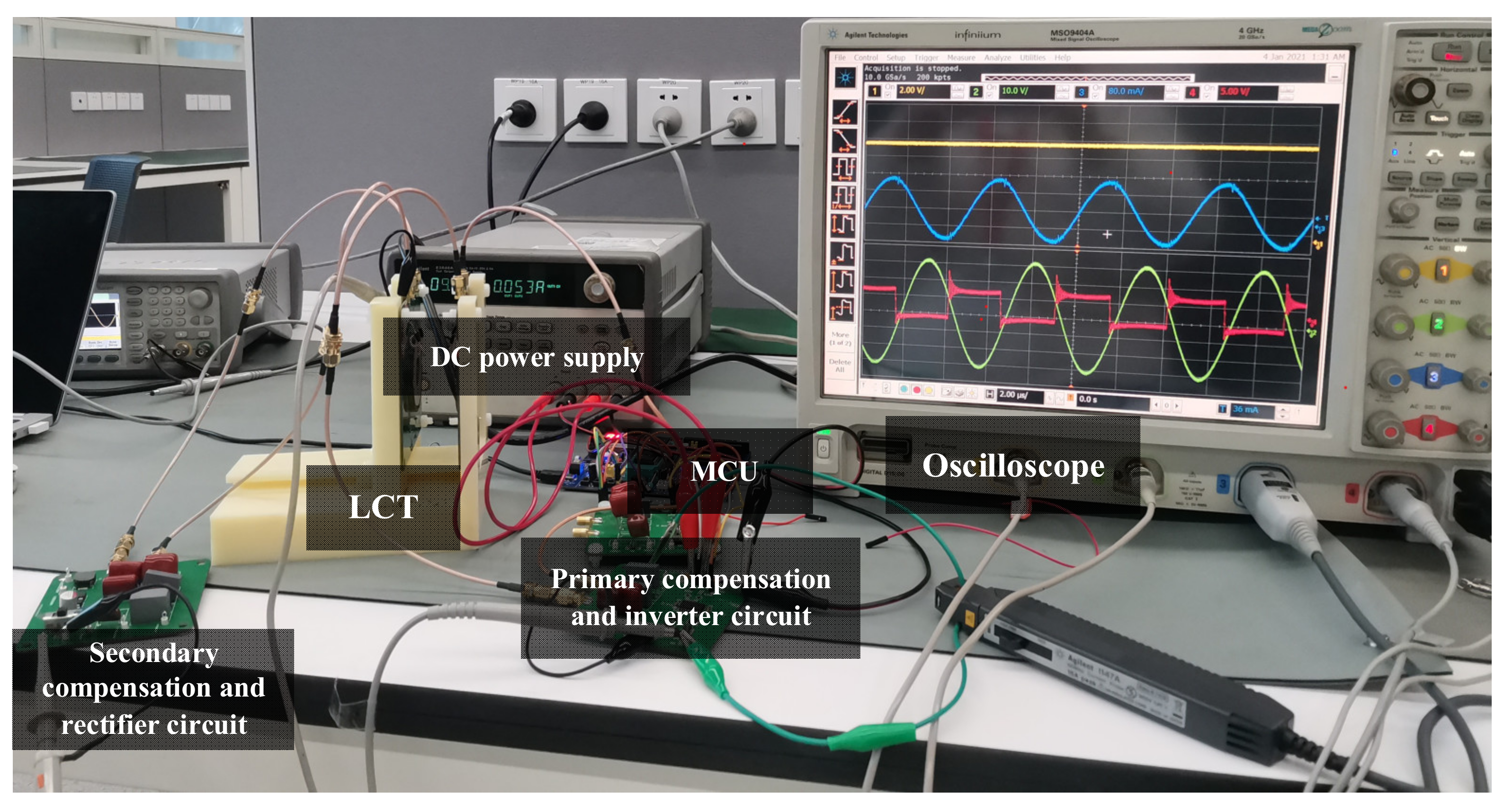
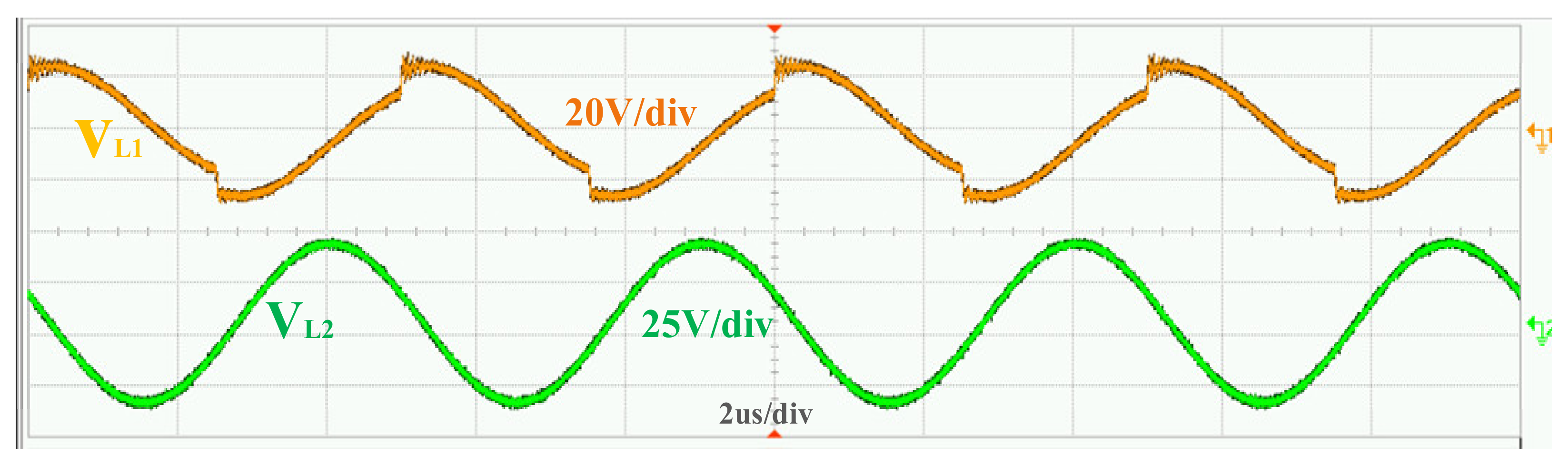
Section 6 demonstrates simulation and experimental results.
Section 7 compares the design methods of this paper with those of other previous works. Finally, the entire work is concluded in
Section 8.
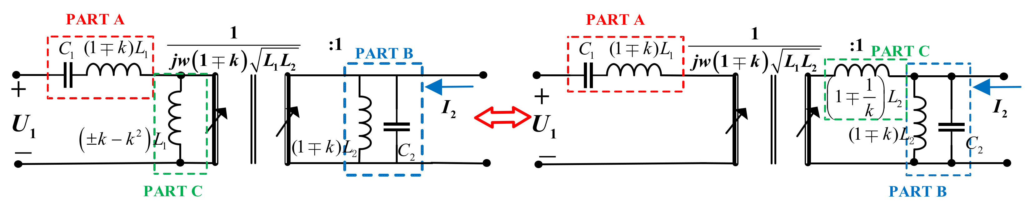
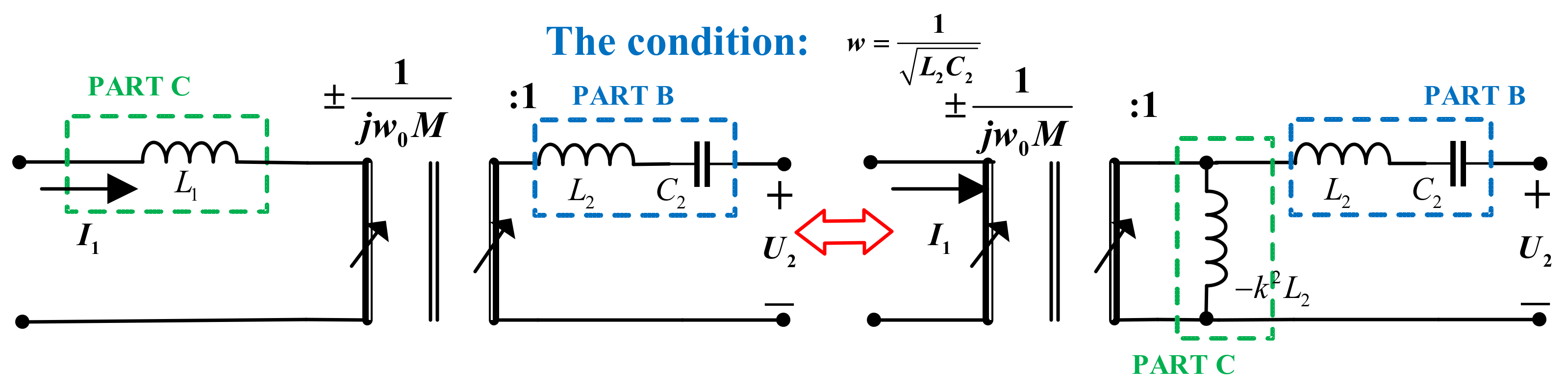
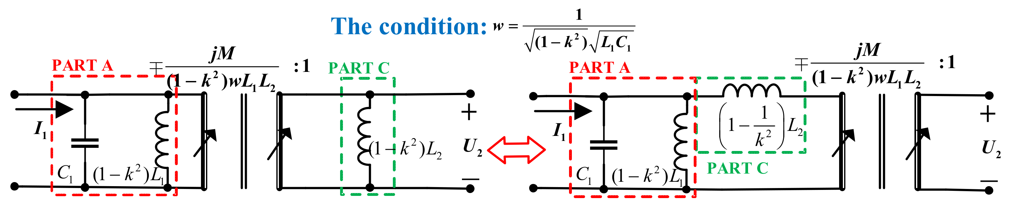
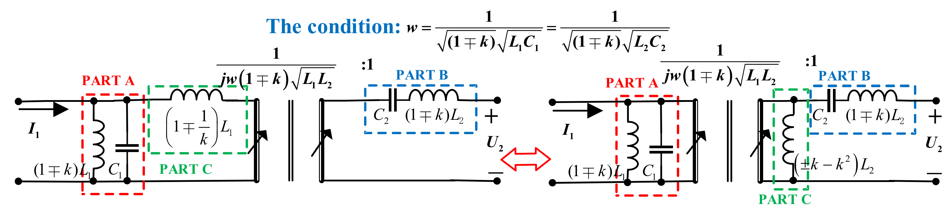
5. Compensation Topology Design Method for IPT System
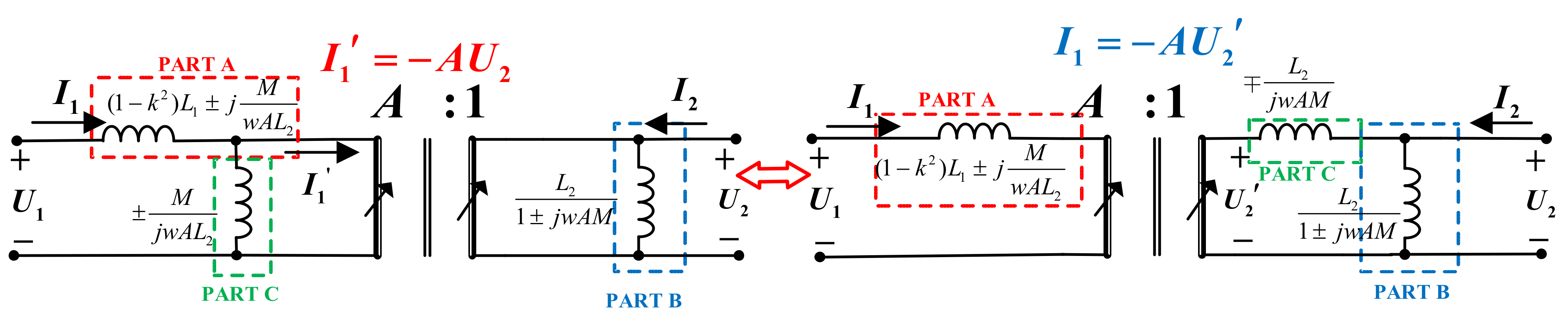
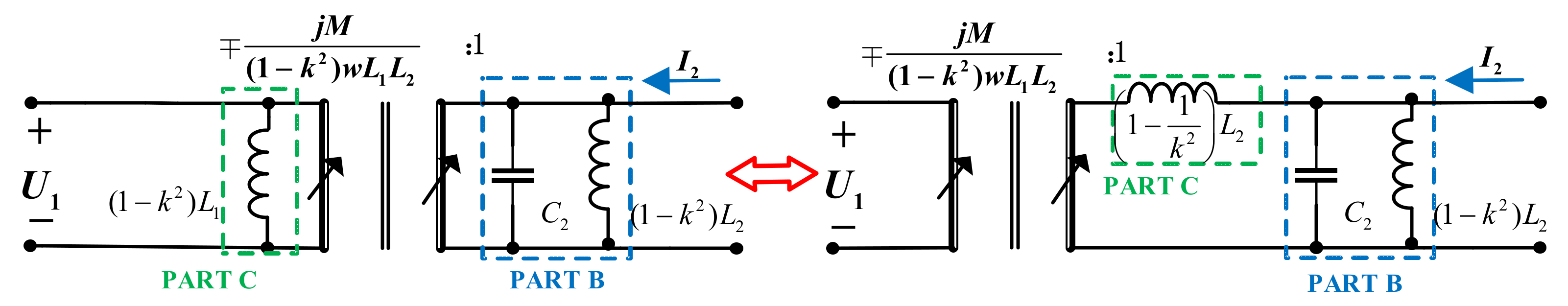
The design methodology for voltage-fed compensation circuit with load-independent CC/CV output at ZPA frequencies is given in detail below. It should be noted that the design method presented in this paper can be easily transplanted to the comprehensive design of the current-fed compensation network.
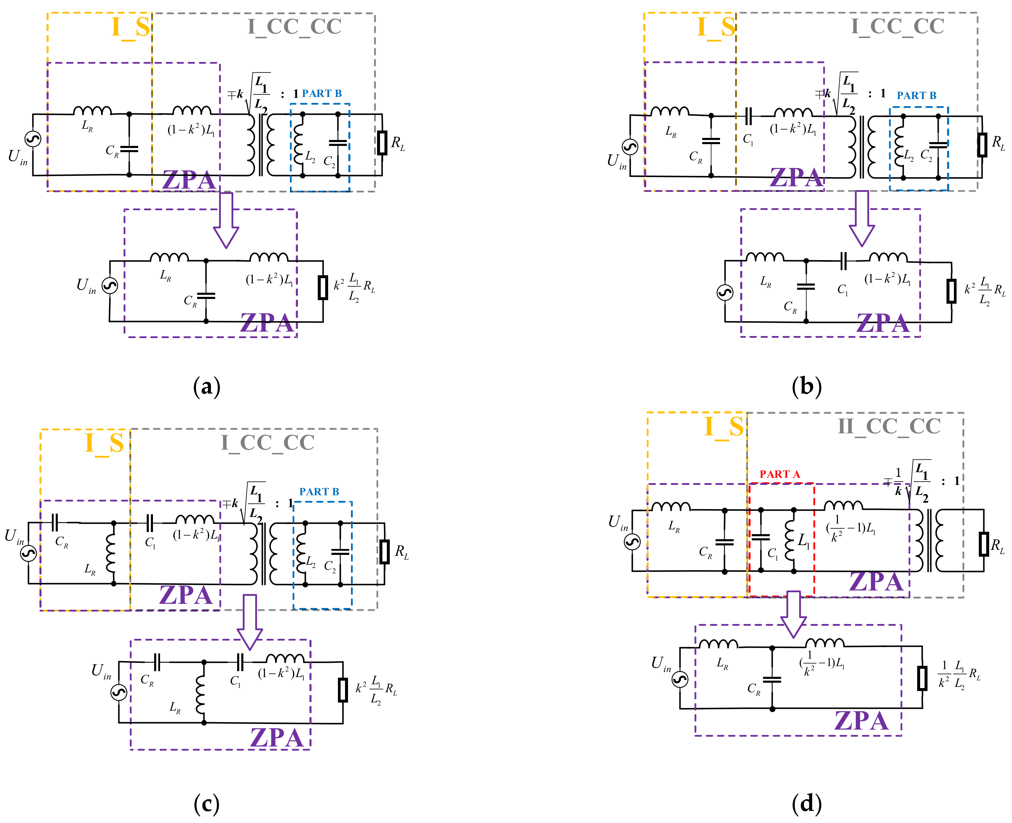
Take voltage-source driving to realize load-independent CC output as an example to illustrate the design method of this article. Combining with the model analysis in
Section 3 and
Section 4, there can be three types of design forms as shown in
Figure 22.
The first type is direct conversion, that is, the CV_CC model of
Section 3.2.
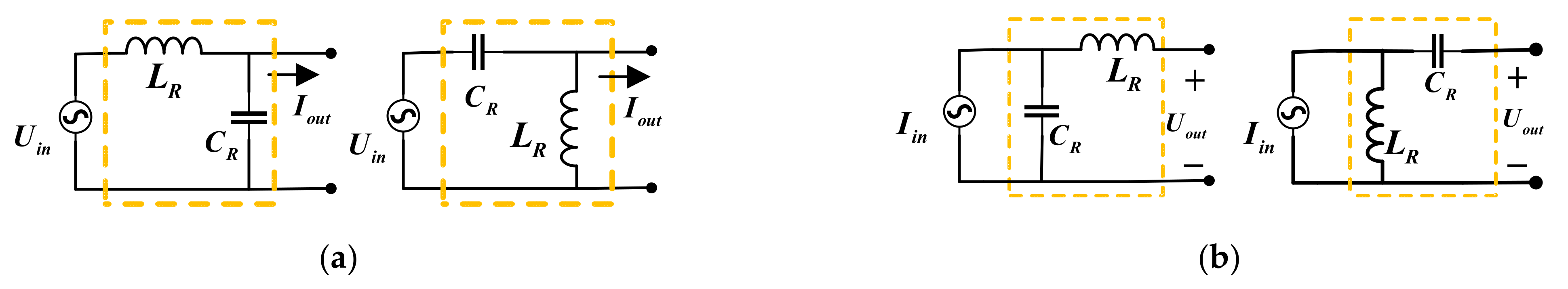
The second type uses the LC/CL resonant tank at the source side to convert voltage to the current, and then the CC_CC model is used to convert to constant current.
The third type uses the CV_CV model to convert voltage to voltage, and the LC/CL resonant tank at the load side is used to convert the voltage to constant current.
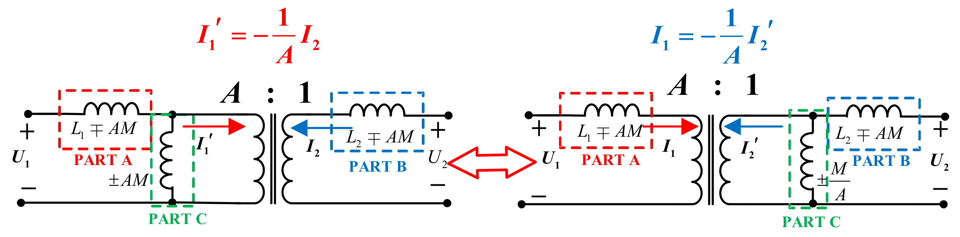
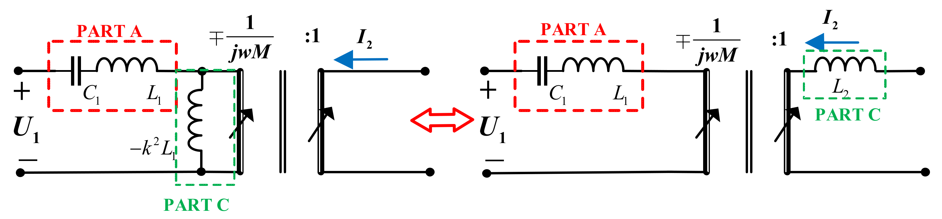
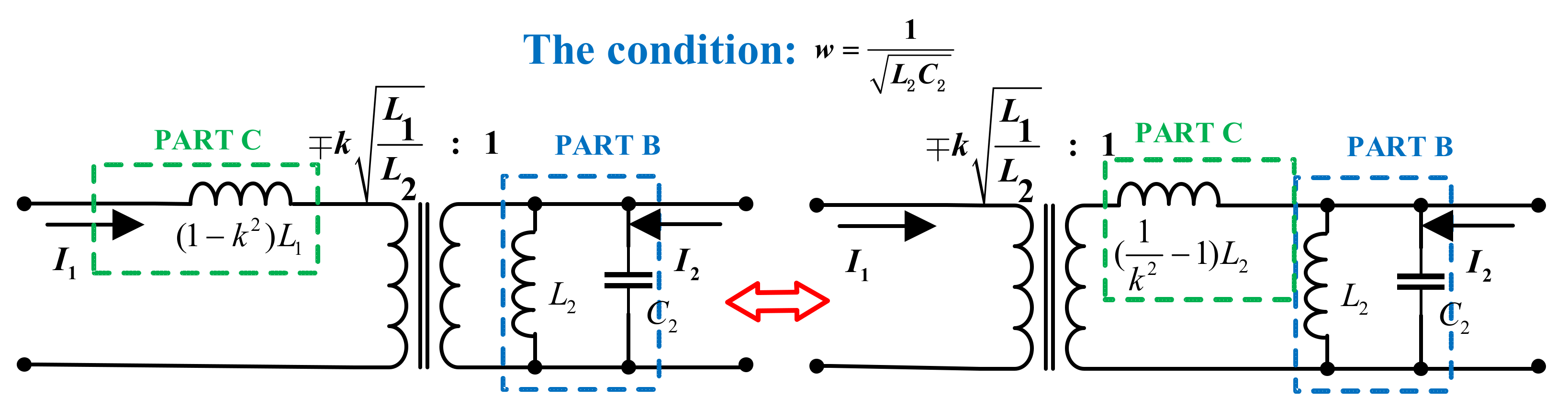
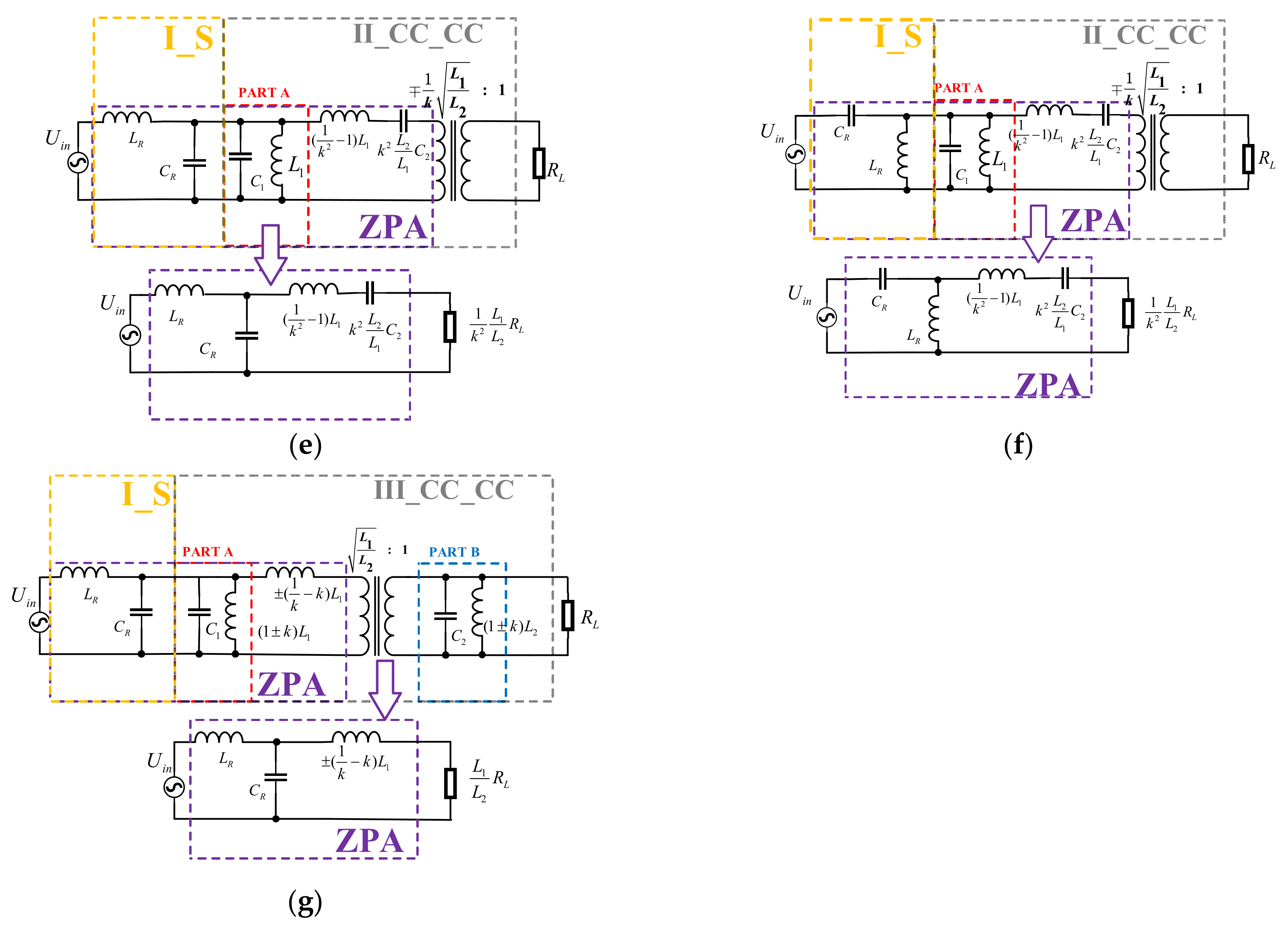
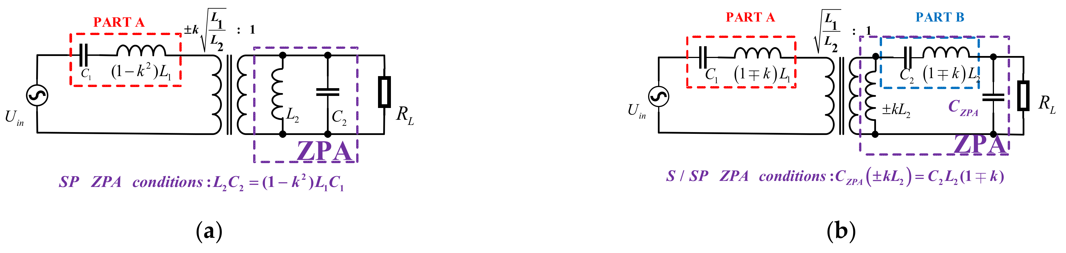
The first type (D_CV_CC): The voltage source cannot drive the parallel topology [
6]; therefore, the I_CV_CC model cannot be directly used to achieve constant voltage to constant current from the source to load. In order to achieve ZPA characteristics, the compensation capacitor can be connected in series on the secondary side of the II_CV_CC/III_CV_CC model, as shown in
Figure 23. The ZPA realization condition is
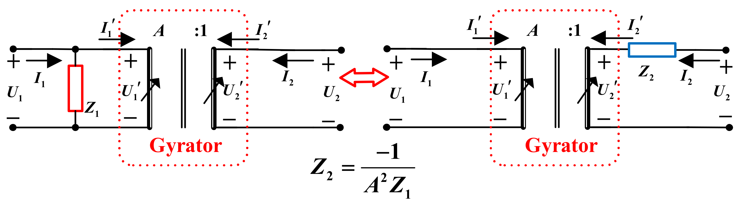
In terms of the current-voltage conversion characteristics of an ideal gyrator, the value of the load-independent transconductance (
) of
Figure 23 is expressed as
A is the transfer ratio of the ideal gyrator.
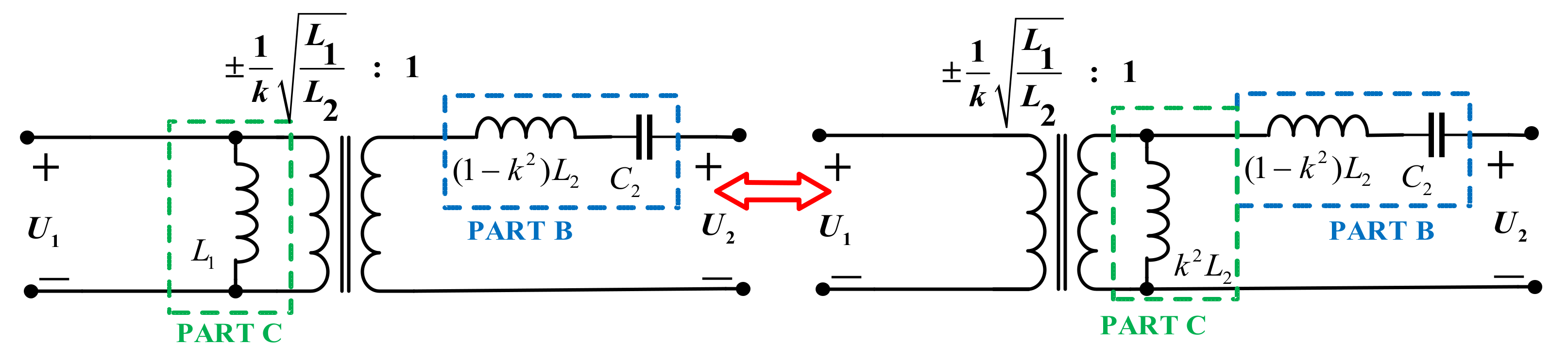
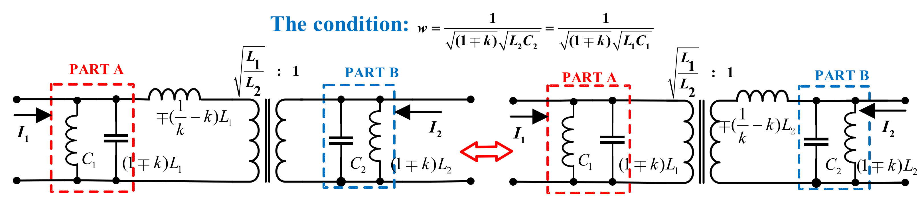
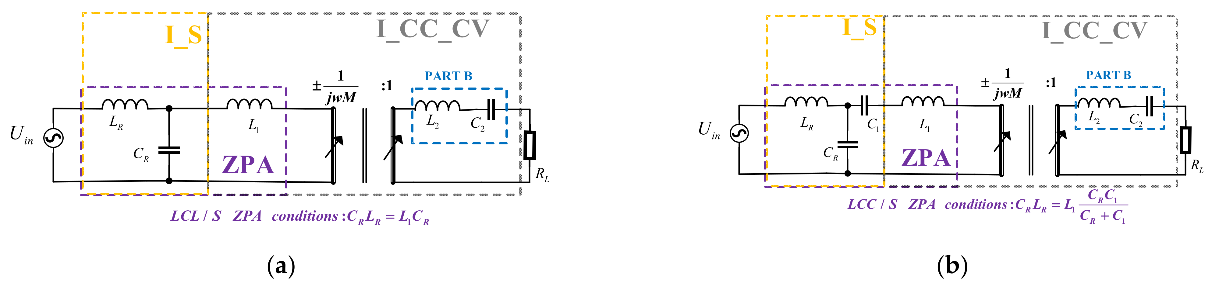
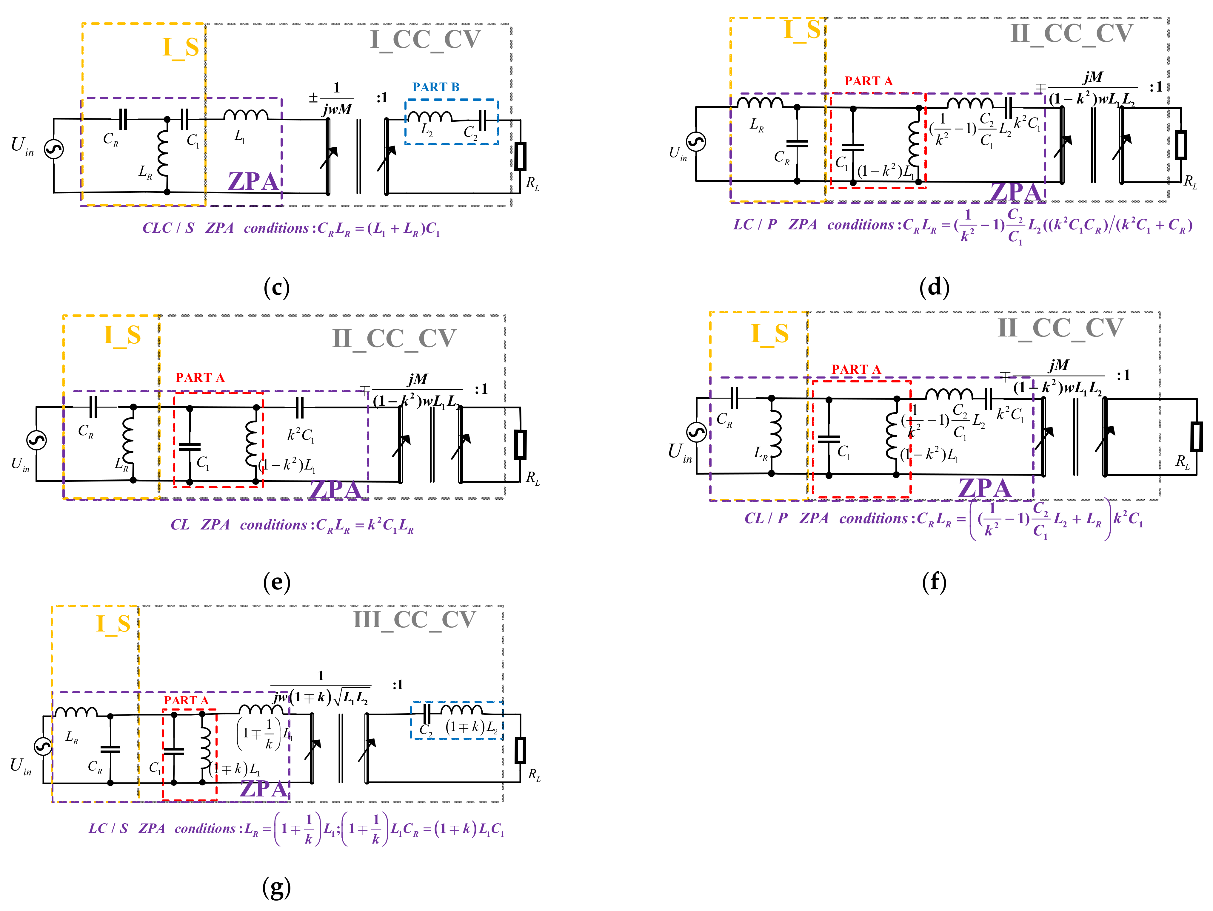
The second type (S_CC_CV): As described above, the source conversion circuits have two options, and the CC_CC model has three types. There is a total of seven design forms as shown in
Figure 24. Among them, LCL/P [
21,
22,
24,
25,
26], LCC/P [
15,
21,
25], CLC/P [
21], LC /S [
27], and LCL/P [
26] have all been analyzed in detail in the previous researches. Two new topologies are designed, namely LC and CLC/S compensation topology. The following seven design forms of ZPA implementation conditions can be converted into the circuits shown in
Figure 23 and
Figure 24a. The Z parameter matrix corresponding to the two-port network in the red box is
, Then, the port input impedance is
.
is the load resistance equivalent to the resistance of the primary stage, which can be expressed as
A is the ratio of the primary voltage to the secondary voltage of an ideal transformer in
Figure 25a. The conditions for the constant-current output of the S_CC_CV type circuit are
resulting in Z
11 = 0. Z
12 and Z
21 are inductive or capacitive components, which result in
not containing imaginary parts. Therefore, in order to make Z
in a pure resistance, the conditions for the establishment of ZPA are
According to (18), the ZPA conditions of LC and CLC/S compensation topology are
The ZPA implementation conditions of other topologies are shown in
Table 3.
The load-independent transconductance (
) of
Figure 24 is expressed as
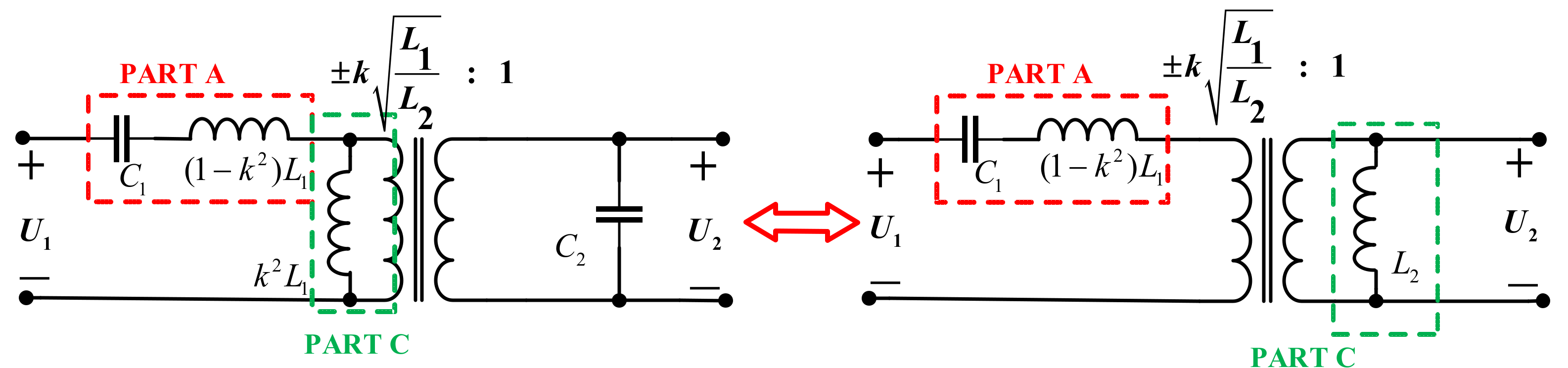
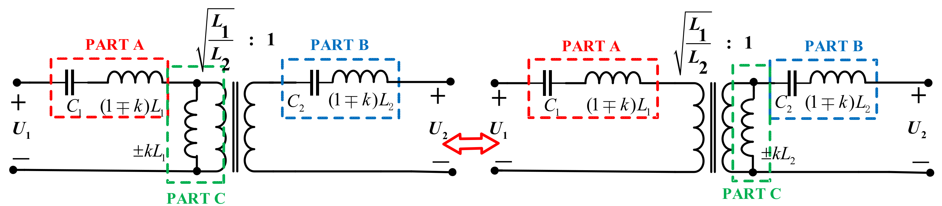
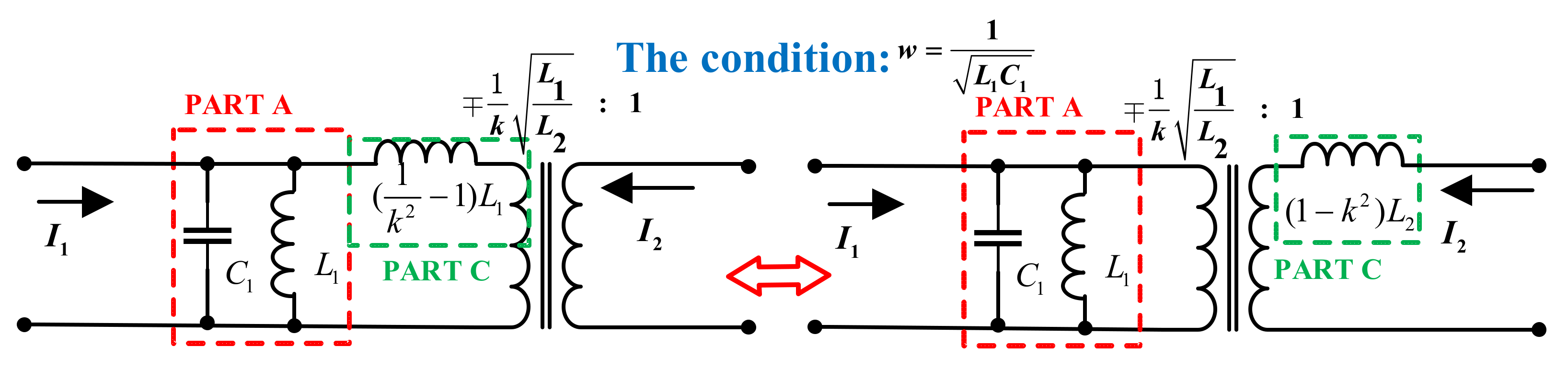
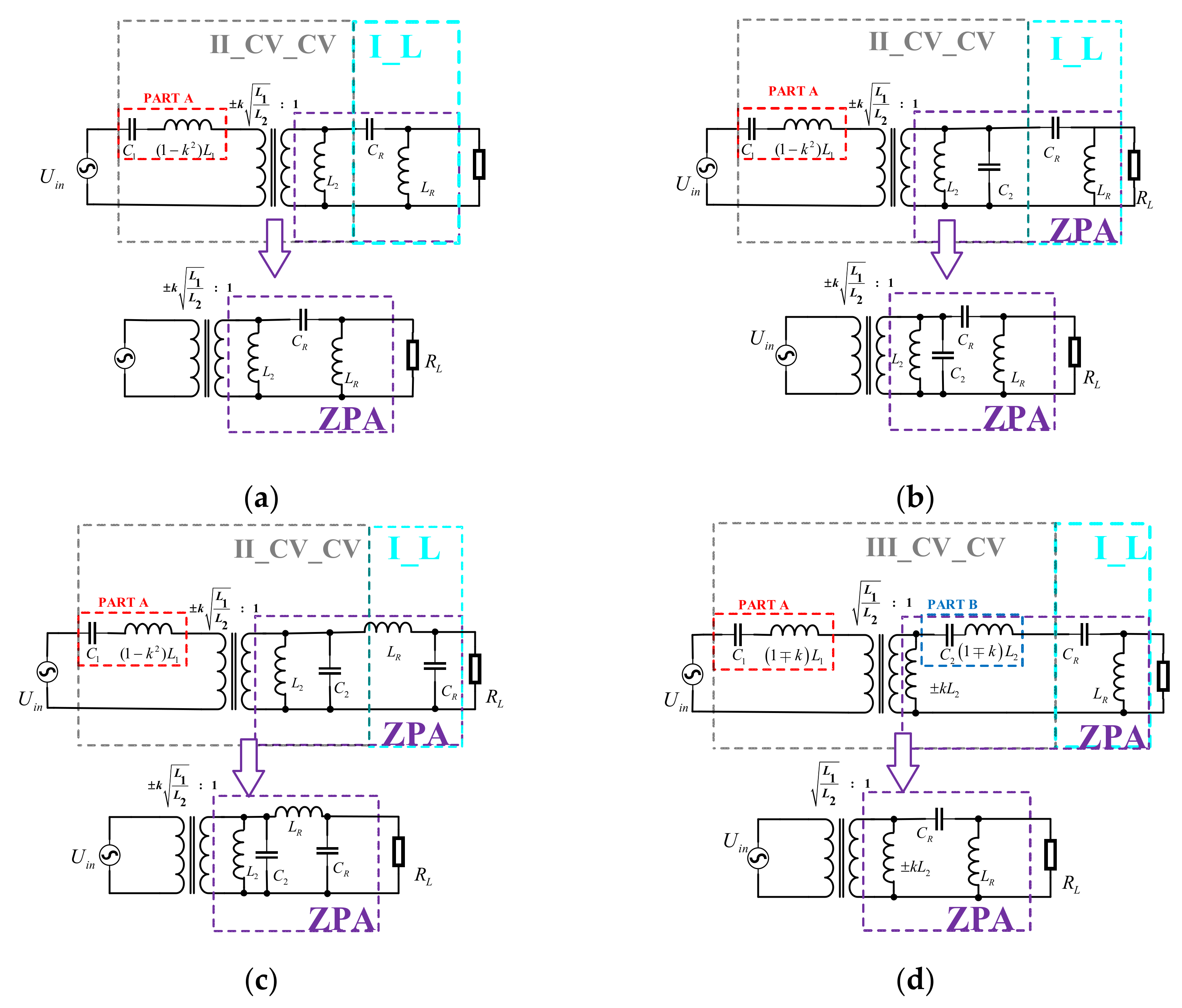
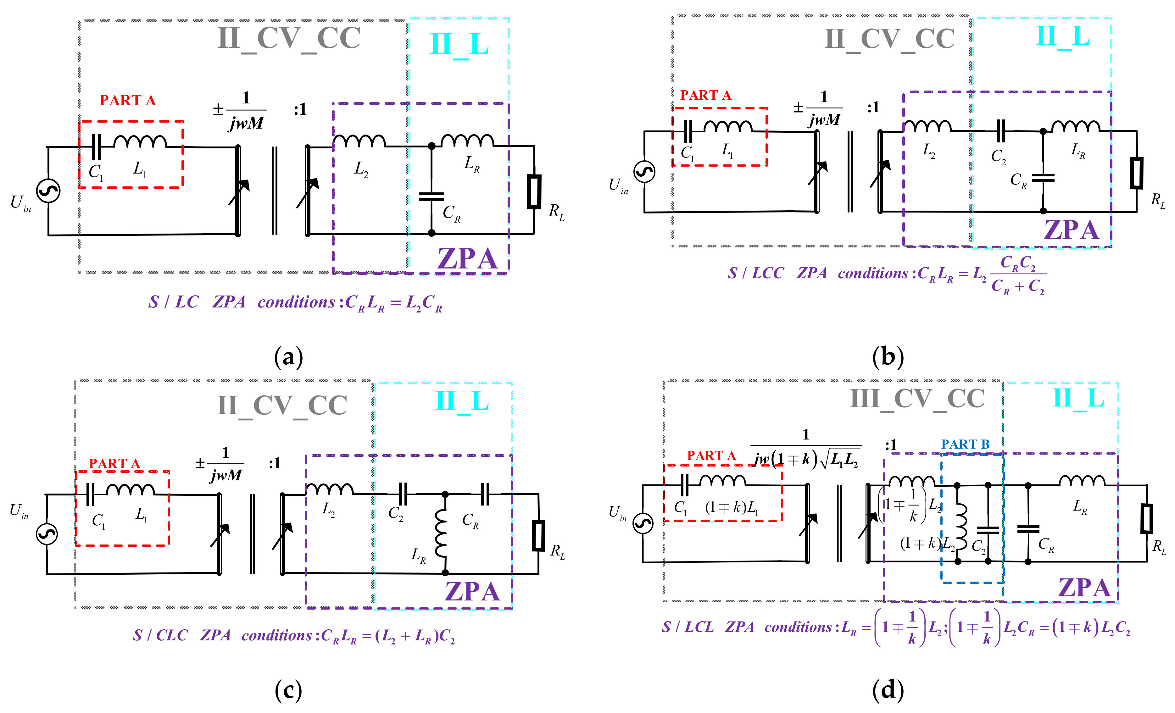
The third type (CV_CV_L): As described above, the CV_CV model has three types, and the load conversion circuits have two options. Four novel compensation topologies are designed as shown in
Figure 26: namely, S/LC, S/LCC, S/CLC, and S/LC. The above compensation topologies of ZPA implementation conditions can be converted into the circuits shown in
Figure 25b and
Figure 26. The Y parameter matrix corresponding to the two-port network in the blue box is
. Then, the port input impedance is
. Similarly, the ZPA realization conditions are
The ZPA implementation conditions of the above compensation topologies are shown in
Table 3.
The load-independent transconductance (
) of
Figure 26 is expressed as:
There are similar design methods for the voltage-fed high-order resonant network to realize load-independent constant-voltage output. The specific design process can be seen in
Figure 27,
Figure 28 and
Figure 29. Detailed design results are shown in
Table 4.
As shown in
Table 3 and
Table 4, for compensation topologies with less than three compensation elements, including S/S compensation, S/PS compensation, S/P compensation, and S/SP compensation, they all have LCT-constrained transfer functions, which means that once the input voltage is determined, the output voltage or current of the system is changed unless the LCT is replaced. However, many applications such as implanted devices have this strict limit on the size of the system space, making that the design of LCT is generally space limited. Therefore, it is difficult to design an LCT to meet all the requirements. Besides, the redesign of LCT is both time and cost consuming.
Compared to these compensation topologies, six novel compensation topologies with LCT-unconstrained CC output characteristics including LC, CLC/S, S/LC, S/LCC, S/CLC, and S/LC and six novel compensation topologies with LCT-unconstrained CV output characteristics including CLC/S, LC/P, CL, CL/P, S/LC, and S/LCC are designed as listed in
Table 3 and
Table 4. It is clear to see that the input–output transfer functions of these compensation topologies depend not only on the parameters of the LCT but also on the value of L
R, which reveals the fact that the output voltage or current can be changed by changing the value of L
R without replacing a new LCT, thus freeing the design from the constraints imposed by the LCT parameters.
In addition, these topologies only require less than four compensation elements, compared to the six compensation elements required for the double-side LCC compensation topology, resulting in a smaller system size, higher power density, and lower cost.
8. Conclusions
In this paper, a simple, comprehensive, and innovative graphical design methodology is proposed for designing compensation circuits to realize load-independent CV or CC output at zero-phase angle (ZPA) frequencies. The proposed approach can be applied to design a set of high-order compensation topologies in a consistent manner. Unlike boring and time-consuming design methods for manipulating circuit equations, using the circuit model given in this paper the load-independent frequency, ZPA conditions, and source-to-load voltage/current gain of the compensation topology can be obtained almost by inspection conveniently, giving a new perspective being free from the constraints of complex equations. Unlike design methods that focus on the analysis of existing compensation topologies, by virtue of the design method in this paper, twelve novel compensation topologies having the input-to-output transfer functions independent of LCT parameters and load-independent CC/CV output are designed and simulated. An S/LCC-compensated IPT system fed by a voltage source with load-independent CV output is designed and manufactured in accordance with the design method of this paper. Simulation and experimental results have shown excellent agreement with the theory. This paper focuses on the compensation topology with constant current or constant voltage under the condition that the coupling coefficient is constant but the load fluctuates greatly, which is suitable for static wireless charging systems with a fixed position. Our future research direction will research the capability of misalignment tolerance of different compensation topologies with load-independent outputs, that is, the sensitivity of the output voltage or current to the change of the coupling coefficient, which will be applied to dynamic wireless power transfer systems.


 ,
, 


