
Unbalanced Two-Way Filtering Power Splitter for Wireless Communication Systems
by
 , ,
, ,
Augustine O. Nwajana
1,* ,
,
Gerald K. Ijemaru
2 ,
,
Kenneth L.-M. Ang
2, 
Jasmine K. P. Seng
3 and
Kenneth S. K. Yeo
4 1
School of Engineering, University of Greenwich, London SE10 9LS, UK
2
School of Science, Technology and Engineering, University of Sunshine Coast, Sunshine Coast, QLD 4556, Australia
3
School of Engineering and Information Technology, University of New South Wales, Sydney, NSW 2052, Australia
4
Department of Electrical and Electronic Engineering, Universiti Teknologi Brunei, Gadong BE1410, Brunei
*
Author to whom correspondence should be addressed.
Electronics 2021, 10(5), 617; https://0-doi-org.brum.beds.ac.uk/10.3390/electronics10050617
Submission received: 14 February 2021
/
Revised: 28 February 2021
/
Accepted: 4 March 2021
/
Published: 6 March 2021
(This article belongs to the Special Issue Advancements in RF, Microwave, and Millimeter-Wave Circuits and Devices)
Abstract
:A compact unbalanced two-way filtering power splitter with an integrated Chebyshev filtering function is presented. The design is purely based on formulations, thereby eliminating the constant need for developing complex optimization algorithms and tuning, to deliver the desired amount of power at each of the two output ports. To achieve miniaturization, a common square open-loop resonator (SOLR) is used to distribute energy between the two integrated channel filters. In addition to distributing energy, the common resonator also contributes one pole to each integrated channel filter, hence, reducing the number of individual resonating elements used in achieving the integrated filtering power splitter (FPS). To demonstrate the proposed design technique, a prototype FPS centered at 2.6 GHz with a 3 dB fractional bandwidth of 3% is designed and simulated. The circuit model and layout results show good performances of high selectivity, less than 1.7 dB insertion loss, and better than 16 dB in-band return loss. The common microstrip SOLR and the microstrip hair-pin resonators used in implementing the proposed integrated FPS ensures that an overall compact size of 0.34 λg × 0.11 λg was achieved, where λg is the guided-wavelength of the 50 Ω microstrip line at the fundamental resonant frequency of the FPS passband.
1. Introduction
The electromagnetic spectrum is becoming more congested and densely occupied with various wireless communication signals, parasitic interferers, and sensing services [1]. More and more sophisticated radiofrequency, microwave, and millimeter-wave filters are required to enable the selection and/or rejection of specific frequency channels. A channel filter (also known as bandpass filter) passes frequencies within a single band while rejecting all other frequencies outside the band [2]. Its main function in the transmitter is to limit the bandwidth of the output signal to the band assigned for the transmission. By this, the transmitter is prevented from interfering with other stations. In the receiver, a bandpass filter permits signals within a certain band of frequencies to be received and decoded, while stopping signals at undesirable frequencies from getting through. A power splitter (PS), on the other hand, is a passive device that makes up one of the essential components within wireless communication systems. Power splitters are often used to direct the correct amount of power to or from other devices (including antennas, multiplexers, filters, and amplifiers) within a wireless system. The overall performance of the system can be significantly influenced by the features of the power splitters within the system [3].
Since filters and power splitters are two essential components often found in modern wireless communication systems, integrating both components into a single device not only reduces the physical footprint of a system, but also reduces cost and losses significantly [4]. This is because an integrated filtering power splitter (FPS) eliminates the need for physically connecting two separate devices using lossy connectors. FPSs have been attracting a lot of attention in recent times as it offers both power distribution and frequency selectivity functions within a wireless communication system. A Wilkinson power divider is one of the most popular and widely used two-way PS due to its simple structure and electrical isolation [1]. This type of power splitter relies on quarter-wavelength transformers to match the output ports as reported in [5]. Several authors have proposed various design techniques for achieving FPS. One state-of-the-art technique is to replace the quarter-wavelength transformers in a Wilkinson power divider with channel filters [6,7,8]. Two-way, single-band filtering power dividers with an unequal output power ratio have been proposed and achieved in [9,10,11]. In Reference [9], the authors relied on modified two-port coupled lines with short-circuit and open-circuit stubs, in achieving an unequal filtering power divider. This technique is effective but very complex when compared to the simple formulae-based design method presented in this paper. In Reference [10], both equal and unequal filtering power dividers were obtained by employing complementary split-ring resonators (CSRRs). The utilization of the CSRRs in the design allows for the filtering function of the power divider. Though the technique was hailed for its effectiveness in achieving miniaturized filtering power divider devices, the FPS reported in this paper is even better in further reducing the device footprint in addition to the design simplicity. Reference [11] reported a modified Wilkinson power divider that uses uniform quarter-wavelength transmission lines for various terminated impedances and arbitrary power ratio. The reported power divider changes only the electrical lengths of the transmission lines between the input and output ports, and those between the output ports and the isolation resistor. The drawback in the design is the lack of filtering characteristics in the device. Hence, an external frequency selective device needs to be physically connected to the power divider, leading to increased size and higher insertion loss when compared to the FPS presented in this paper. Integrated filtering power dividers exhibiting dual/multi-band filtering characteristics has also been reported [12,13,14].
The integrated filtering power splitter/divider reported in this paper is designed to unequally split the input power between the two output ports in the ratio of 1:2. This means that 1/3 of the input power would be channeled towards one port, leaving the other port with 2/3 of the input power. The main contribution/originality of the power splitter/divider proposed in this paper is that its realization is based on simple novel formulations. Hence, results can easily be reproduced by researchers or design engineers all over the world just by simply choosing their design specifications and utilizing the proposed formulations. Another benefit of the proposed work, when compared to those reported in [6,7,8,9,10,11,12,13,14] is it does not rely on tuning and optimization to achieve matching at the three input/output ports. Microstrip technology is used in the implementation of the FPS in order to validate the circuit model through layout simulation.
2. Circuit Model Design
The proposed integrated FPS was formed using two separate, but identical three-pole channel filters designed following the technique reported in [15]. The design specification for the channel filters are as follows: Center frequency f0, 2.6 GHz; fractional bandwidth FBW, 3% and passband return loss of 20 dB. A 3-pole Chebyshev lowpass prototype (i.e., g0 = g4 = 1.0; g1 = g3 = 0.8516; and g2 = 1.1032) with a passband ripple of 0.04321 dB was chosen for this design. The circuit model for the proposed integrated FPS is shown in Figure 1. A2 & A3 and B2 & B3 shown in Figure 1 are the second and third resonators of the first and second channel filters, respectively. CR is the common resonator which replaces the first resonator of each channel filter. Hence, CR contributes one pole to each filtering channel of the FPS. Z0 is the 50 Ohms characteristic impedance of each termination. The values for the J-inverters (i.e., J01 & J23), the capacitor C, and the inductor L were all calculated from [15] using Equations (1) and (2). The main contribution of this paper lies on the formulation for calculating the values of the J-inverters, J1 and J2 shown in Figure 1 using Equation (3). The formulations ensure that the input power from CR is distributed through the two channel filters in the ratio of 1:2. The calculated design parameters for the two-way FPS are all given in Table 1.
The circuit model of Figure 1 was simulated using the Keysight Advanced Design System (ADS). Before performing the simulation, the couplings between resonators were modeled using the method presented in [16], which involves replacing each J-inverter on the circuit model with a pi-network of capacitors as shown in Figure 2. The circuit model simulation results are shown in Figure 3. The results clearly show that the FPS has its center frequency at 2.6 GHz and its minimum return loss at 20 dB as designed. The 3 dB FBW of 3% is also achieved with S21 = −1.7 dB and S31 = −4.7 dB.
3. Microstrip Layout Design
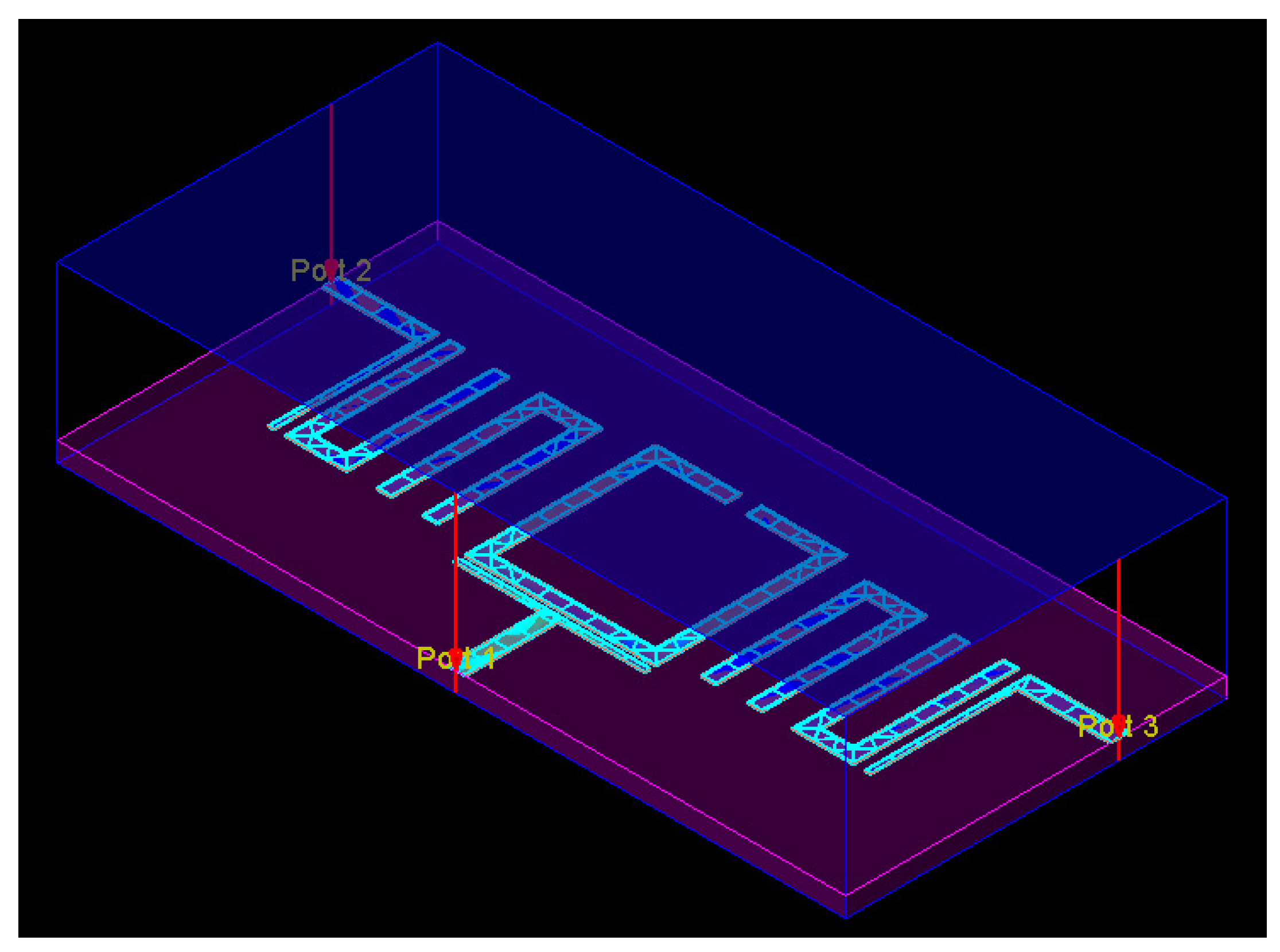
The microstrip square open-loop resonator (SOLR) [17,18,19] and hairpin resonator (HPR) [20] were used in the layout implementation of the proposed FPS. The SOLR and each HPR were designed to resonate at f0. The FPS layout was made on Rogers RT/Duroid 6010LM substrate with a relative dielectric constant ɛr = 10.7, thickness h = 1.27 mm, and loss tangent tan δ = 0.0023. The physical dimensions of the FPS were determined using the Keysight ADS full-wave electromagnetic simulator. The coupling scheme and the equivalent microstrip layout, indicating the simulated dimensions, are shown in Figure 4. The k23 in Figure 4a is the coupling coefficient between each pair of channel filter resonators while Qext is the external quality factor between CR and port 1, and the last resonator of each channel filter and their respective ports (i.e., ports 2 & 3). Each port represents a 50 Ohms termination. The values for k23 and Qext in Figure 4a were all calculated from [15] using Equation (4), where f1 and f2 are the eigenmodes from simulating a pair of microstrip resonators. The calculated values for k1 and k2 were determined using Equation (5). These values (i.e., k1 and k2) ensure that 1/3 and 2/3 of the input power are delivered to ports 2 and 3, respectively. Figure 4b shows the simulated dimensions for achieving the unbalanced FPS layout:
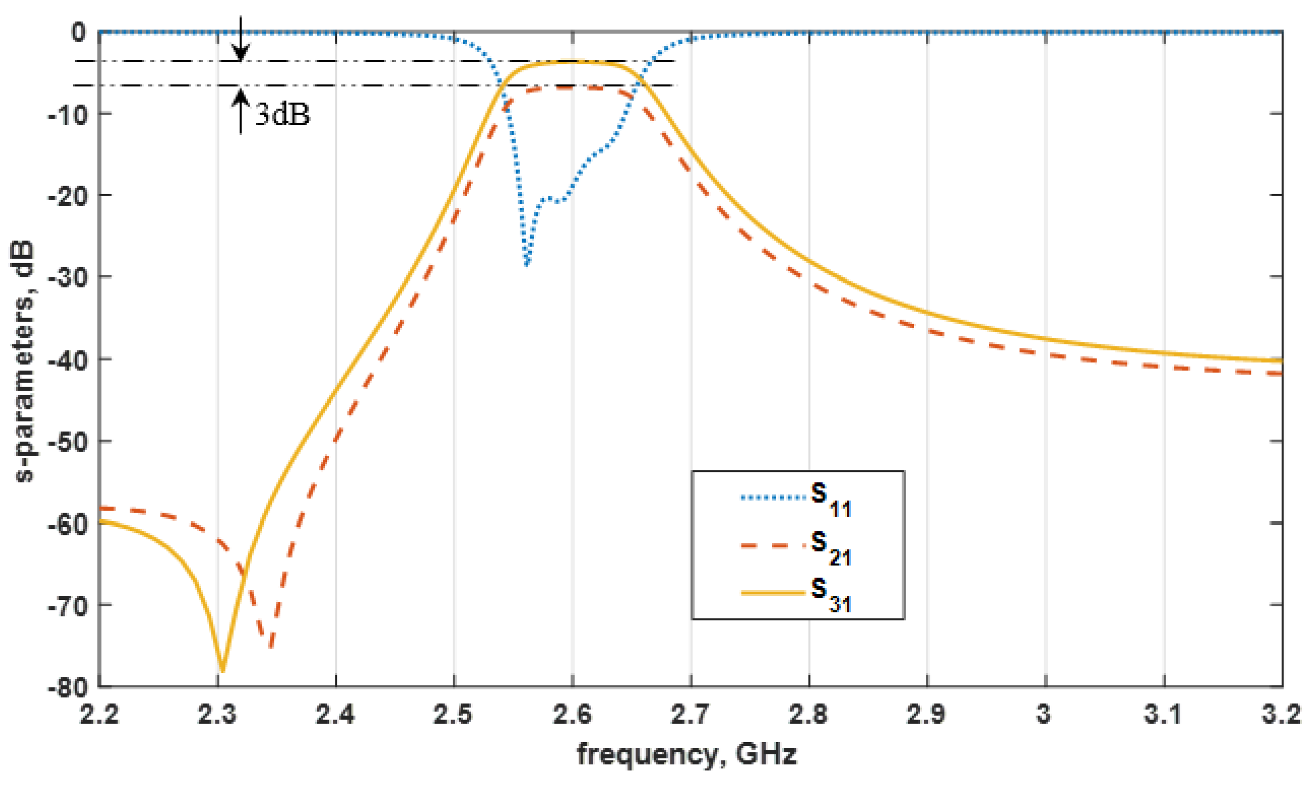
The FPS layout of Figure 4b was simulated using the Keysight ADS Momentum full-wave electromagnetic simulator. The simulation results are shown in Figure 5 and confirms that the FPS has its center frequency at 2.6 GHz, with a simulated minimum return loss at 16 dB. The 3 dB FBW of 3% is also indicated in the results of Figure 5. S21 and S31 indicate transmission zeros at 2.31 GHz and 2.34 GHz, respectively. It is important to note that, unlike the FPS circuit model design that is lossless, the microstrip layout implementation includes both conductor and dielectric losses. The loss tangent of the of the dielectric materials was kept at 0.0023, while the copper conductivity used for the simulation is maintained at 5.8 × 10⁷ S/m, with a thickness of 35 micron (µm) for both the top and bottom metals of the microstrip line. Surface roughness and thickness variation of the substrate material were not considered. A photograph of the fabricated microstrip FPS is shown in Figure 6.
4. Results Comparison and Discussion
The circuit model and microstrip layout results of the proposed FPS are co-presented in Figure 7 for easy comparison. The results show good agreement with a good insertion loss of less than 1.7 dB, a minimum in-band return loss of greater than 16 dB, and the center frequency of 2.6 GHz, as designed. The 3D momentum visualization (in ADS) of the simulated FPS layout, with visible mesh and current distribution at 2.6 GHz, are shown in Figure 8. A performance comparison with some related works [9,10,11,21,22,23] is presented in Table 2 and shows that the proposed FPS is of compact size, 0.0374 (λg)2, where λg is the guided-wavelength of the 50 Ω microstrip line at the fundamental resonant frequency of the FPS passband.
5. Conclusions
An unbalanced two-way integrated filtering power splitter was proposed, designed, and implemented using the microstrip transmission line technology. The design is completely based on novel simple formulations and relies on microstrip square open-loop and hair-pin resonators for miniaturization. The proposed filtering power splitter unequally splits the input power between the two output ports in the ratio of 1:2, meaning that 1/3 of the input power is channeled towards one port, leaving the other port with 2/3 of the input power. The proportionate splitting of power between the two filtering channels happens at the common square open-loop resonator (SOLR). This common resonator also contributes one pole to each channel and hence, adds to the device miniaturization. The circuit model and microstrip layout results showed good agreement with a center frequency of 2.6 GHz, insertion loss of less than 1.7 dB, and minimum return loss of greater than 16 dB. The FPS is of a compact size and occupies an overall footprint of 39 mm by 13 mm, i.e., 0.34 λg × 0.11 λg, where λg is the guided wavelength of the 50 Ω microstrip line at 2.6 GHz. Further work on the proposed FPS could include employing the substrate integrated waveguide (SIW) technology [24] for design implementation. By this, both the insertion and return losses could be further improved. The downside is that when the SIW technology is utilized, the device footprint would be relatively large when compared to the microstrip implementation employed in this paper. As reported in [1], design engineers are often required to compromise between several conflicting requirements, as it is rather difficult or even physically and/or electrically impossible to simultaneously achieve all the desired design specifications.
Author Contributions
Conceptualization, A.O.N. and K.S.K.Y.; methodology, A.O.N. and K.S.K.Y.; software, A.O.N.; validation, A.O.N.; formal analysis, A.O.N.; investigation, A.O.N.; writing—original draft preparation, A.O.N.; writing—review and editing, K.L.-M.A. and J.K.P.S.; visualization, G.K.I.; supervision, K.S.K.Y., J.K.P.S., and K.L.-M.A.; project administration, A.O.N. and G.K.I. All authors have read and agreed to the published version of the manuscript.
Funding
This research received no external funding.
Acknowledgments
The authors would like to thank Keysight Technologies for providing, at a nominal cost, the ADS software tool used for conducting all the simulations in this project.
Conflicts of Interest
The authors declare no conflict of interest.
References
- Chen, X.-P.; Wu, K. Substrate integrated waveguide filter: Basic design rules and fundamental structure features. IEEE Microw. Mag. 2014, 15, 108–116. [Google Scholar] [CrossRef]
- Nwajana, A.O.; Dainkeh, A.; Yeo, K.S.K. Substrate integrated waveguide (SIW) bandpass filter with novel microstrip-CPW-SIW input coupling. J. Microw. Optoelectron. Electromagn. Appl. 2017, 16, 393–402. [Google Scholar] [CrossRef]
- Mirzaei, M.; Sheikhi, A. Design and implementation of microstrip dual-band filtering power divider using square-loop resonator. Electron. Lett. 2020, 56, 19–21. [Google Scholar] [CrossRef]
- Liu, S.; Zhang, G.; Ding, Z.; Zhang, Z. Miniaturised wide tuning-range four-way quasi-lumped-element filtering power divider. Electron. Lett. 2020, 56, 825–828. [Google Scholar] [CrossRef]
- Dainkeh, A.; Nwajana, A.O.; Yeo, K.S.K. Filtered power splitter using square open loop resonators. Prog. Electromagn. Res. C 2016, 64, 133–140. [Google Scholar] [CrossRef] [Green Version]
- Chi, P.-L.; Chen, Y.-M.; Yang, T. Single-layer dual-band balanced substrate- integrated waveguide filtering power divider for 5G millimeter-wave applications. IEEE Microw. Wirel. Compon. Lett. 2020, 30, 585–588. [Google Scholar] [CrossRef]
- Li, H.-Y.; Xu, J.-X.; Yang, Y.; Zhang, X.Y. Novel switchable filtering circuit with function reconfigurability between SPQT filtering switch and four-way filtering power divider. IEEE Trans. Microw. Theory Tech. 2019, 68, 867–876. [Google Scholar] [CrossRef]
- Nwajana, A.O.; Otuka, R.I.; Ebenuwa, S.H.; Ihianle, I.K.; Aneke, S.O.; Edoh, A.A. Symmetric 3dB filtering power divider with equal output power ratio for communication systems. In Proceedings of the 2nd International Conference on Electrical, Communication, and Computer Engineering (ICECCE), Istanbul, Turkey, 14–15 April 2020; pp. 1–4. [Google Scholar]
- Zhuang, Z.; Wu, Y.; Jiao, L.; Wang, W.; Liu, Y. Wideband balanced-to-unbalanced filtering unequal power divider with wide stopband and isolation. Electron. Lett. 2017, 53, 892–894. [Google Scholar] [CrossRef]
- Danacian, M.; Moznebi, A.-R.; Afrooz, K.; Hakimi, H. Miniaturised equal/unequal SIW power divider with bandpass response loaded by CSRRs. Electron. Lett. 2016, 52, 1864–1866. [Google Scholar] [CrossRef]
- Yoon, Y.-C.; Kim, Y. Modified Wilkinson power divider using transmission lines for various terminated impedances and arbitrary power ratio. J. Electromagn. Eng. Sci. 2019, 19, 42–47. [Google Scholar] [CrossRef] [Green Version]
- Chen, L.; Wei, F.; Cheng, X.Y.; Xiao, Q.K. A dual-band balanced-to-balanced power divider with high selectivity and wide stopband. IEEE Access 2019, 7, 40114–40119. [Google Scholar] [CrossRef]
- Zhang, G.; Zhang, X.; Liu, S.; Tang, L.; Yang, J.; Hong, J.-S. Tri-band filtering power divider based on multi-mode fork-type resonator for performance enhancement. IET Microw. Antennas Propag. 2020, 14, 867–873. [Google Scholar] [CrossRef]
- Dong, G.; Wang, W.; Wu, Y.; Liu, Y.; Fang, Y.; Tantzeris, M.M. Compact dual-band filtering power divider with independently controllable bandwidths using shorted patch resonators. IET Microw. Antennas Propag. 2020, 14, 759–767. [Google Scholar] [CrossRef]
- Nwajana, A.O.; Yeo, K.S.K.; Dainkeh, A. Low cost SIW Chebyshev bandpass filter with new input/output connection. In Proceedings of the 16th Mediterranean Microwave Symposium (MMS), Abu Dhabi, United Arab Emirates, 14–16 November 2016; pp. 1–4. [Google Scholar]
- Hong, J.-S. Microstrip Filters for RF/Microwave Applications, 2nd ed.; John Wiley & Sons: Hoboken, NJ, USA, 2011. [Google Scholar]
- Nwajana, A.O.; Yeo, K.S.K. Microwave diplexer purely based on direct synchronous and asynchronous coupling. Radioengineering 2016, 25, 247–252. [Google Scholar] [CrossRef]
- Hong, J.-S.; Lancaster, M.J. Coupling of microstrip square open-loop resonators for cross-coupled planar microwave filters. IEEE Trans. Microw. Theory Tech. 1996, 44, 2099–2109. [Google Scholar] [CrossRef]
- Nwajana, A.O.; Yeo, K.S.K. Multi-coupled resonator microwave diplexer with high isolation. In Proceedings of the 46th European Microwave Conference (EuMC), London, UK, 3–7 October 2016; pp. 1167–1170. [Google Scholar]
- Nwajana, A.O. Circuit modelling of bandpass/channel filter with microstrip implementation. Indones. J. Electr. Eng. Inform. 2020, 8, 696–705. [Google Scholar]
- Chen, C.-J.; Ho, Z.-C. Design equations for a coupled-line type filtering power divider. IEEE Trans. Microw. Theory Tech. 2017, 27, 257–259. [Google Scholar] [CrossRef]
- Wang, Y.; Xiao, F.; Cao, Y.; Zhang, Y.; Tang, X. Novel wideband microstrip filtering power divider using multiple resonators for port isolation. IEEE Access 2019, 7, 61868–61873. [Google Scholar] [CrossRef]
- Lyn, Y.-P.; Zhu, L.; Cheng, C.-H. A new design of filtering power dividers with arbitrary constant phase difference, impedance transformation, and good isolation. IEEE Access 2019, 7, 169495–169507. [Google Scholar]
- Nwajana, A.O.; Dainkeh, A.; Yeo, K.S.K. Substrate integrated waveguide (SIW) diplexer with novel input/output coupling and no separate junction. Prog. Electromagn. Res. 2018, 67, 75–84. [Google Scholar] [CrossRef] [Green Version]
Figure 1.
Circuit model with J-inverters and identical inductor-capacitor resonators.

Figure 2.
Circuit model with J-inverters as capacitor-only network.

Figure 3.
Results of the unbalanced filtering power splitter circuit model.

Figure 4.
Unbalanced two-way filtering power splitter: (a) Coupling scheme with Qext = 28.387, k23 = 0.031, k1 = 0.018, and k2 = 0.025; (b) microstrip layout with all dimensions in mm.
Figure 4.
Unbalanced two-way filtering power splitter: (a) Coupling scheme with Qext = 28.387, k23 = 0.031, k1 = 0.018, and k2 = 0.025; (b) microstrip layout with all dimensions in mm.

Figure 5.
Results of the microstrip filtering power splitter layout.

Figure 6.
Photograph of the fabricated microstrip filtering power splitter.

Figure 7.
Comparison of the circuit model and the microstrip layout results (a) differential-mode responses and (b) single-ended output ports responses.
Figure 7.
Comparison of the circuit model and the microstrip layout results (a) differential-mode responses and (b) single-ended output ports responses.

Figure 8.
Three-dimensional momentum visualization of the proposed unbalanced filtering power splitter with visible mesh and current distribution at 2.6 GHz.
Figure 8.
Three-dimensional momentum visualization of the proposed unbalanced filtering power splitter with visible mesh and current distribution at 2.6 GHz.


Table 1.
This Calculated Circuit Model Design Parameters.
| L (nH) | C (pF) | J01 | J23 | J1 | J2 |
|---|---|---|---|---|---|
| 0.1078 | 34.7529 | 0.02 | 0.0176 | 0.0101 | 0.0143 |
Table 2.
Calculated circuit model design parameters.
| Ref. | f0 (GHz) | Filter Order | Size (λg) 2 | FP 1 | PSR 2 | IL 3 (dB) |
|---|---|---|---|---|---|---|
| [9] | 2.00 | 3 | 0.1209 | Yes | 1:2 | 1.97 |
| [10] | 5.73 | 2 | 0.0480 | Yes | 1:4 | 1.70 |
| [11] | 2.00 | - | 0.1091 | No | 1:2 | 2.00 |
| [21] | 1.00 | 2 | 0.0612 | Yes | 1:2 | 3.80 |
| [22] | 1.99 | 3 | 0.0825 | Yes | 1:2 | 3.74 |
| [23] | 3.00 | 3 | 0.2166 | Yes | 1:2 | 1.78 |
| This work | 2.60 | 3 | 0.0374 | Yes | 1:2 | 1.70 |
1. Filtering property. 2. Power splitting ratio. 3. Insertion loss.
Publisher’s Note: MDPI stays neutral with regard to jurisdictional claims in published maps and institutional affiliations. |
© 2021 by the authors. Licensee MDPI, Basel, Switzerland. This article is an open access article distributed under the terms and conditions of the Creative Commons Attribution (CC BY) license (http://creativecommons.org/licenses/by/4.0/).
Share and Cite
MDPI and ACS Style
Nwajana, A.O.; Ijemaru, G.K.; Ang, K.L.-M.; Seng, J.K.P.; Yeo, K.S.K. Unbalanced Two-Way Filtering Power Splitter for Wireless Communication Systems. Electronics 2021, 10, 617. https://0-doi-org.brum.beds.ac.uk/10.3390/electronics10050617
AMA Style
Nwajana AO, Ijemaru GK, Ang KL-M, Seng JKP, Yeo KSK. Unbalanced Two-Way Filtering Power Splitter for Wireless Communication Systems. Electronics. 2021; 10(5):617. https://0-doi-org.brum.beds.ac.uk/10.3390/electronics10050617
Chicago/Turabian StyleNwajana, Augustine O., Gerald K. Ijemaru, Kenneth L.-M. Ang, Jasmine K. P. Seng, and Kenneth S. K. Yeo. 2021. "Unbalanced Two-Way Filtering Power Splitter for Wireless Communication Systems" Electronics 10, no. 5: 617. https://0-doi-org.brum.beds.ac.uk/10.3390/electronics10050617
Note that from the first issue of 2016, this journal uses article numbers instead of page numbers. See further details here.