
Dual-Band, Dual-Output Power Amplifier Using Simplified Three-Port, Frequency-Dividing Matching Network


School of Electronic Engineering, Beijing University of Posts and Telecommunications, Beijing 100876, China
*
Author to whom correspondence should be addressed.
Electronics 2022, 11(1), 144; https://0-doi-org.brum.beds.ac.uk/10.3390/electronics11010144
Submission received: 6 December 2021
/
Revised: 26 December 2021
/
Accepted: 30 December 2021
/
Published: 4 January 2022
(This article belongs to the Special Issue Feature Papers in Circuit and Signal Processing)
Abstract
:This study presents a dual-band power amplifier (PA) with two output ports using a simplified three-port, frequency-dividing matching network. The dual-band, dual-output PA could amplify a dual-band signal with one transistor, and the diplexer-like output matching network (OMN) divided the two bands into different output ports. A structure consisting of a λ/4 open stub and a λ/4 transmission line was applied to restrain undesired signals, which made each branch equivalent to an open circuit at another frequency. A three-stub design reduced the complexity of the OMN. Second-order harmonic impedances were tuned for better efficiency. The PA was designed with a 10-W gallium nitride high electron mobility transistor (GaN HEMT). It achieved a drain efficiency (DE) of 55.84% and 53.77%, with the corresponding output power of 40.22 and 40.77 dBm at 3.5 and 5.0 GHz, respectively. The 40%-DE bandwidths were over 200 MHz in the two bands.
1. Introduction
With the development of wireless communication systems, people have been seeking methods for higher data rates. It is essential to increase spectral efficiency because spectrum resources are limited. As a result, the research on RF transmitters that can operate on multiple bands has attracted more attention. Power amplifiers (PAs) are necessary parts of RF transmitters. Therefore, one of the research trends focuses on how to design PAs that can operate over multiple frequencies, such as multiband [1,2,3,4,5,6,7], broadband [8,9,10,11,12], and band-tunable PAs [13]. Existing studies have achieved multiband operation in different conditions. For example, Refs. [1,2] present dual-band and quad-band PAs in MMIC using on-chip impedance transformers, and Refs. [3,4,5] implemented a dual-band characteristic within a Doherty PA structure. Some studies investigated different ways of matching multiband impedance. Dai et al. [6] explored a direct solving method for triband matching networks. Meng et al. [7] reported a synthesis method that could create dual-band impedance rotation to increase the bandwidth and gain flatness of PAs.
Carrier aggregation (CA) and multiple-input multiple-output (MIMO) are important technologies to improve spectral efficiency. CA utilizes different bands within the available spectrum, whether they are contiguous, noncontiguous, or broadly separated. MIMO multiplies transmission and receiving antennas, which may work on different carrier frequencies for better radiation pattern performance [14,15]. In carrier aggregation MIMO front ends, multiple PAs are needed to feed every antenna element on its working frequency, which causes higher costs.
A new type of multiband PA that has multiple output ports was presented recently [16]. A dual-band, dual-output PA was designed for the dual-band case. It could perform as a dual-array feed network with its diplexer-like output matching network (OMN) [17]. It worked like a general dual-band PA that could amplify a dual-band signal with one transistor. The difference is that it could separate the signal into two single-band signals and send them into two different output ports by its OMN. The architecture of the PA is shown in Figure 1. It had a power-added efficiency (PAE) of 40.4%/39.9% and an output power of 36.7/37.1 dBm at 3.5/5.5 GHz. The methodology used in Ref. [16] to achieve the specially featured OMN was an iterative process of tuning, and no harmonic termination was conducted in the design, which limited its efficiency. Therefore, the design simplicity and performance of the original work need to be further improved.
This study presents a newly designed dual-band, dual-output PA with a detailed matching procedure and a generalized design methodology. The output matching uses a simplified three-port, frequency-dividing matching network to miniaturize the circuit and reduce its complexity. A structure consisting of a λ/4 open stub and a λ/4 transmission line was applied to prevent the signal from passing through improperly. Second-order harmonic impedances were tuned for better efficiency. A 10-W gallium nitride high electron mobility transistor (GaN HEMT) was used to deliver more power. Finally, the newly designed PA achieved a drain efficiency (DE) of 55.84%/53.77% and output power of 40.22/40.77 dBm at 3.5/5.0 GHz. Moreover, the two branches could create stopband rejections of more than 24.4 dB at 3.5 GHz and 38.6 dB at 5 GHz.
2. Design Methodology
2.1. Restraining Network
The two branches in the frequency-dividing matching network were required to prevent signals in the other band from passing through. The restraining network shown in Figure 2 was applied for that purpose. It consisted of an open-circuit stub and a transmission line.
The open-circuit stub with the characteristic impedance Z2 and the electrical length θ2 was used to create a short-circuit condition for minimizing the influence of the OMN with the input impedance Zin1 when they were connected in parallel. The transmission line with the characteristic impedance Z1 and the electrical length θ1 transferred the short-circuit condition to an open-circuit condition.
As shown in Figure 2, the input impedance of the branch with the restraining network can be written as:
where
The input impedance of the open-circuit stub was determined by
Combining Equations (1)–(3), Zin can be calculated as
When θ2 = 90°, the effect of Zin1 on Zin vanishes. Moreover, if θ1 = 90°, the restraining network will make the branch behave as an open circuit.
In the branch of f1, lengths of the open-circuit stub and the transmission line were set as λ/4 at f2. Then the branch will be equivalent to an open circuit at f2. At the same time, Zin at f1 will be
By setting a proper OMN after the restraining network, Zin could be tuned to the optimal impedance of the transistor.
2.2. Design of Output Matching Network
For higher efficiency and output power, a Cree Wolfspeed 10 W CGH40010F (CREE, Durham, NC, USA) packaged GaN HEMT was used for the design. The two operating frequencies were 3.5 GHz (f1) and 5.0 GHz (f2) near the widely used sub-6 GHz 5G bands.
The first step of designing the three-port, frequency-dividing output matching network was finding the optimal impedance for the transistor. Using the nonlinear transistor model provided by the manufacturer, the simulated load-pull results at fundamental, second-order, and third-order harmonic frequencies are presented in Figure 3. Contours were taken at the package plane of the transistor. Under consideration of output power and PAE, the targeted input impedances of OMN were chosen near 12 Ω at f1 and 10 Ω at f2.
The topology of the dual-band, dual-output PA is schematically shown in Figure 4. The two branches of the OMN had the optimal impedance to the transistor at its working frequency. Simultaneously, it behaved as an open circuit at another frequency, which prevented the branch from affecting the impedance at that frequency and guaranteed that signals in the other band would not interfere with its output. The restraining networks (TL9,11 and TL10,12) were applied for this condition.
For better efficiency, harmonic tuning networks were employed after the restraining networks. Results in Figure 3c,d show that the second-order harmonic impedances positively influenced the performance. In contrast, the impact of the third-order harmonic impedances was much lower. Therefore, second-order harmonic impedance was tuned by this network, which means the proposed PA works in the class-J mode.
In the harmonic tuning network, a λ/8 open stub (TL15 and TL16) was used to create a short-circuited condition at the second-order harmonic frequency for the connecting point. Furthermore, the tuning line (TL13 and TL14) tuned the condition at the package plane to be the proper impedance with the restraining network.
Stub-tuned matching networks (TL17,19 and TL18,20) were applied after the harmonic tuning networks to make each branch match the optimal impedance of its operating frequency. The two branches were connected to make the three-port OMN. The restraining networks eliminated the interaction between the two branches at fundamental frequencies. However, the harmonic impedances may be influenced. Moreover, the blocking capacitor (C3), RF choke (L2), and soldering pad also affected impedances, so optimization was needed after the connection. Figure 5a depicts the input impedances of each branch after optimization, and Figure 5b shows the input impedances of the three-port OMN, which were well matched to the region of high performance. All the impedances were simulated with the external components and circuits. The results imply that the fundamental impedances were near the point before the connection. However, the second-order and third-order harmonic impedances are changed at different degrees.
The two branches were bent forward to reduce the size of the dual-output power amplifier and to balance the performance. The layout of the designed three-port, frequency-dividing OMN is shown in Figure 6a. The three-stub branches lowered the complexity compared to the design in Ref. [16]. S-parameters of the three-port OMN are depicted in Figure 6b. The restraining networks created isolation of more than 40 dB between different bands, which ensured the high performance of the PA in working bands. Furthermore, the output ports isolation was also better than 40 dB near the working frequency.
2.3. Design of Input Matching Network
Unlike the three-port OMN, the input matching network was a traditional dual-band matching network. Figure 7a shows the layout of it. The design of the input network refers to the dual-band matching technology based on compact broadband matching networks presented in Ref. [7]. The input network consisted of three open stubs and three transmission lines. Three stubs and two connecting lines (TL1–TL5) created a dual-band impedance rotation. The rest line (TL6) made the impedance move to the proper position.
For stabilization, a parallel RC circuit (C2 and R1) at the gate and a resistor (R2) before the gate bias line were added. After iterative optimizations, the network had the optimal impedance for the transistor in the working bands, and the stability factor satisfied the unconditionally stable requirement in the whole frequency range. Figure 7b depicts the impedances of the input matching network from 3.2 to 5.2 GHz with simulated source-pull contours of PAE at f1/ f2.
3. Fabrication and Measurement
The proposed dual-band, dual-output PA shown in Figure 8a was performed on a 30-mil Rogers RO4350B (Rogers, Chandler, AZ, USA) substrate with a relative permittivity of 3.66 and a loss tangent of 0.0037, using a 10-W Cree CGH40010F GaN HEMT (CREE, Durham, NC, USA). The OMN was loaded with a 4310LC wideband RF choke. The transistor was biased and stabilized at a drain-source voltage (VDS) of 28 V, and the quiescent drain current (IDS) was 168 mA, which was selected in the class-AB region. The lumped-element capacitors used for blocking and stabilizing were Murata GRM18 series chip multilayer ceramic capacitors.
Figure 8b demonstrates the test environment for the designed PA. An Agilent N5182A vector signal generator (Agilent, Santa Clara, NC, USA) was used to provide a CW signal. The signal was pre-amplified by a driver amplifier, since the output power of the generator was not enough to drive the PA. The output of the PA was measured by an Agilent N9030A signal analyzer (Agilent, Santa Clara, NC, USA). A 40-dB attenuator was added between the output port of the PA and the signal analyzer to prevent the large signal from exceeding the input limit of the analyzer. When one port is being measured, another should be connected to a 50-Ω load to accord with practice.
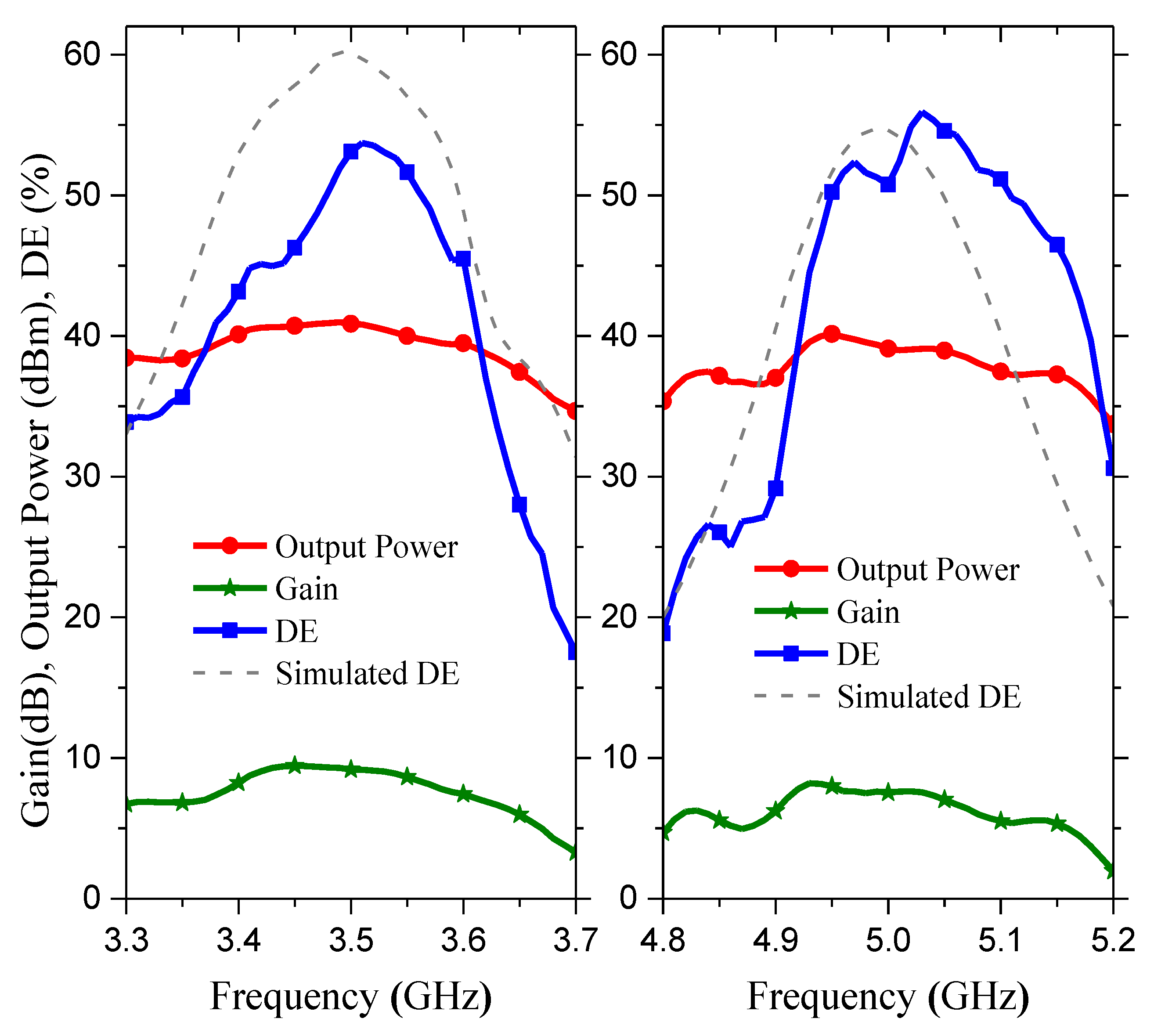
The measured gain, output power, and DE of the proposed PA at f1 and f2 are depicted in Figure 9. At 3.5 GHz, the DE reached 55.84% when Pin = 31.7 dBm, with an output power of 40.2 dBm, and the small-signal gain was 11.6 dB. At 5.0 GHz, the DE reached 53.77% when Pin = 33 dBm, with an output power of 40.7 dBm, and the small-signal gain was 9.8 dB. Figure 10 gives the gain of the two output ports at the undesired frequencies. The stopband rejections of the two branches were better than 24.4 dB at 3.5 GHz and 38.6 dB at 5 GHz.
Figure 11 shows the performance over the two bands. The PA had a bandwidth of 200 MHz over 40% efficiency near 3.5 and 5 GHz. The measured efficiency was lower than simulated results in the lower band. There were slight frequency shifts in both bands, which may have been caused by the impact of manufacturing variations and device deviation. The conductor width tolerance of the manufacturer was 0.02 mm, and the amplitude accuracy of the signal analyzer was ±0.19 dB. It is found in experiments that the curvature of the circuit board can affect the performance. Therefore, more advanced manufacturing and better auxiliary accessories are needed for better performance.
To evaluate the linearity, the proposed PA was tested with a 10-MHz WCDMA signal with a peak-to-average power ratio (PAPR) of 6.6 dB. Figure 12 shows the measured normalized power spectra. The output power is 31.9/30.6 dBm in the two bands. When digital predistortion (DPD) is on, the adjacent channel power ratio (ACPR) is −47.0/−48.1 dBc, respectively. The DPD used a generalized memory polynomial model based on a negative feedback iteration technique.
Table 1 displays the results of this work together with other recent studies of dual-band PAs. Due to the nature of the unique dual-output architecture and the high operation frequencies, the PA proposed in this study cannot be directly compared to other single-output works [3,7,18,19,20,21]. Nevertheless, the dual-output PAs have a wider noncontiguous absolute bandwidth (2.0 and 1.5 GHz) than the single-output PAs, and the high working frequencies are closer to the widely used sub-6 GHz 5G bands that will predominate in future wireless communications. Compared to the previous work in dual-band, dual-output PAs, this PA has better efficiencies and gain at the two operating frequencies, closer to the normal dual-band PA. Moreover, the simple structure and the generalized design methodology will make the PA extensible, easier to design, and have more potential for practical uses.
4. Conclusions
A dual-band, dual-output power amplifier designed with a simplified three-port, frequency-dividing matching network was presented in this study. The OMN with two branches could send signals in different bands into different output ports using restraining networks that prevented unwanted signals from passing through. In each branch, second-order harmonics were controlled for better efficiency. The PA with a 10-W CGH40010F packaged GaN HEMT achieved a DE of 55.84%/53.68% and output power of 40.22/40.77 dBm at 3.5/5.0 GHz. It can be expected that the high performance, simple structure, and generalized design methodology will make this PA extensible and have more potential for practical uses.
5. Patents
The corresponding Chinese patent (no. 202010299317.5) of this work has already been granted.
Author Contributions
Conceptualization, Y.W. and X.C.; methodology, X.C.; software, X.C.; validation, X.C., Y.W., and W.W.; formal analysis, X.C. and Y.W.; investigation, Y.W.; resources, Y.W. and W.W.; data curation, X.C.; writing—original draft preparation, X.C.; writing—review and editing, Y.W. and W.W.; visualization, X.C.; supervision, Y.W. and W.W.; project administration, W.W.; funding acquisition, Y.W. and W.W. All authors have read and agreed to the published version of the manuscript.
Funding
This research was supported by National Natural Science Foundations of China (No.61971052, U21A20510, and No. U20A20203) and the Fundamental Research Funds for the Central Universities (2021XD-A07-1).
Data Availability Statement
The data presented in this study are available within the article.
Conflicts of Interest
The authors declare no conflict of interest.
References
- Yin, Y.; Xiong, L.; Zhu, Y.; Chen, B.; Min, H.; Xu, H. A compact dual-band digital polar Doherty power amplifier using parallel-combining transformer. IEEE J. Solid-State Circuits 2019, 54, 1575–1585. [Google Scholar] [CrossRef]
- Park, J.; Lee, C.; Park, C. A quad-band CMOS linear power amplifier for EDGE applications using an anti-phase method to enhance its linearity. IEEE Trans. Circuits Syst. I Regul. Papers 2017, 64, 765–776. [Google Scholar] [CrossRef]
- Liu, M.; Fang, X.; Huang, H.; Boumaiza, S. Dual-band 3-way Doherty power amplifier with extended back-off power and bandwidth. IEEE Trans. Circuits Syst. II Express Briefs 2020, 67, 270–274. [Google Scholar] [CrossRef]
- Liu, H.-Y.; Zhai, C.; Cheng, K.-K.M. Novel dual-band equal-cell Doherty amplifier design with extended power back-off range. IEEE Trans. Microw. Theory Tech. 2020, 68, 1012–1021. [Google Scholar] [CrossRef]
- Yang, Z.; Li, M.; Yao, Y.; Dai, Z.; Li, T.; Jin, Y. Design of concurrent dual-band continuous Class-J mode Doherty power amplifier with precise impedance terminations. IEEE Microw. Wirel. Compon. Lett. 2019, 29, 348–350. [Google Scholar] [CrossRef]
- Dai, Z.; Pang, J.; Li, M.; Li, Q.; Peng, J.; He, S. A Direct Solving Approach for High-Order Power Amplifier Matching Network Design. IEEE Trans. Microw. Theory Tech. 2020, 68, 3278–3286. [Google Scholar] [CrossRef]
- Meng, X.; Yu, C.; Wu, Y.; Liu, Y. Design of dual-band high-efficiency power amplifiers based on compact broadband matching networks. IEEE Microw. Wirel. Compon. Lett. 2018, 28, 162–164. [Google Scholar] [CrossRef]
- Zhuang, Z.; Wu, Y.; Yang, Q.; Kong, M.; Wang, W. Broadband power amplifier based on a generalized step-impedance quasi-chebyshev lowpass matching approach. IEEE Trans. Plasma Sci. 2020, 48, 311–318. [Google Scholar] [CrossRef]
- Krishnamoorthy, R.; Kumar, N.; Grebennikov, A.; Ramiah, H. A high-efficiency ultra-broadband mixed-mode GaN HEMT power amplifier. IEEE Trans. Circuits Syst. II Express Briefs 2018, 65, 1929–1933. [Google Scholar] [CrossRef]
- Chen, H.; Xu, J.-X.; Kong, Z.-H.; Chen, W.-H.; Zhang, X.Y. Broadband High-Efficiency Power Amplifier With Quasi-Elliptic Low-Pass Response. IEEE Access 2020, 8, 52566–52574. [Google Scholar] [CrossRef]
- Saxena, S.; Rawat, K.; Roblin, P. Continuous class-B/J power amplifier using a nonlinear embedding technique. IEEE Trans. Circuits Syst. II Express Briefs 2017, 64, 837–841. [Google Scholar] [CrossRef]
- Ghisotti, S.; Pisa, S.; Colantonio, P. S Band Hybrid Power Amplifier in GaN Technology with Input/Output Multi Harmonic Tuned Terminations. Electronics 2021, 10, 2318. [Google Scholar] [CrossRef]
- Azam, A.; Bai, Z.; Walling, J.S. Leveraging programmable capacitor arrays for frequency-tunable digital power amplifiers. IEEE Trans. Microw. Theory Tech. 2020, 68, 1983–1994. [Google Scholar] [CrossRef]
- Choi, J.; Hwang, W.; You, C.; Jung, B.; Hong, W. Four-element reconfigurable coupled loop MIMO antenna featuring LTE full-band operation for metallic-rimmed smartphone. IEEE Trans. Antennas Propag. 2019, 67, 99–107. [Google Scholar] [CrossRef]
- Zou, H.; Li, Y.; Shen, H.; Wang, H.; Yang, G. Design of 6 × 6 dual-band MIMO antenna array for 4.5 G/5G smartphone applications. In Proceedings of the 2017 Sixth Asia-Pacific Conference on Antennas and Propagation (APCAP), Xi’an, China, 16–19 October 2017; pp. 1–3. [Google Scholar]
- Cappello, T.; Duh, A.; Barton, T.W.; Popovic, Z. A dual-band dual-output power amplifier for carrier aggregation. IEEE Trans. Microw. Theory Tech. 2019, 67, 3134–3146. [Google Scholar] [CrossRef]
- Duh, A.; Rahimizadeh, S.; Barton, T.; Popović, Z. A 3.5/5.9-GHz dual-band output matching network for an efficiency-optimized multiband power amplifier. In Proceedings of the 2018 IEEE Topical Conference on RF/Microwave Power Amplifiers for Radio and Wireless Applications (PAWR), Anaheim, CA, USA, 14–17 January 2018; pp. 75–78. [Google Scholar]
- Huang, H.; Zhang, B.; Yu, C.; Gao, J.; Wu, Y.; Liu, Y. A novel analytic design method of dual-band harmonic-tuned power amplifiers. Microw. Opt. Technol. Lett. 2018, 60, 2496–2500. [Google Scholar] [CrossRef]
- Chen, W.; Zhang, S.; Liu, Y.; Liu, Y.; Ghannouchi, F.M. A concurrent dual-band uneven Doherty power amplifier with frequency-dependent input power division. IEEE Trans. Circuits Syst. I Regul. Papers 2014, 61, 552–561. [Google Scholar] [CrossRef]
- Saad, P.; Colantonio, P.; Piazzon, L.; Giannini, F.; Andersson, K.; Fager, C. Design of a concurrent dual-band 1.8–2.4-GHz GaN-HEMT Doherty power amplifier. IEEE Trans. Microw. Theory Tech. 2012, 60, 1840–1849. [Google Scholar] [CrossRef]
- Kalyan, R.; Rawat, K.; Koul, S.K. A digitally assisted dual-input dual-band Doherty power amplifier with enhanced efficiency and linearity. IEEE Trans. Circuits Syst. II Express Briefs 2019, 66, 297–301. [Google Scholar] [CrossRef]
Figure 1.
Block diagram of the dual-band, dual-output PA presented in Ref. [16].
Figure 1.
Block diagram of the dual-band, dual-output PA presented in Ref. [16].

Figure 2.
Circuit model of the proposed restraining network.

Figure 3.
Simulated load-pull results at (a) the fundamental frequency of f1, (b) the fundamental frequency of f2, (c) second-order harmonic frequencies, and (d) third-order harmonic frequencies.
Figure 3.
Simulated load-pull results at (a) the fundamental frequency of f1, (b) the fundamental frequency of f2, (c) second-order harmonic frequencies, and (d) third-order harmonic frequencies.

Figure 4.
Block diagram of the harmonically tuned dual-band, dual-output PA. Output port1 output signals at f1 = 3.5 GHz. Output port2 output signals at f2 = 5.0 GHz. C1 = 20 pF, C3 = 20 pF, C2 = 3 pF, R1 = R2 = 50 Ω, L1 = 18 nH, L2 = 1 uH.
Figure 4.
Block diagram of the harmonically tuned dual-band, dual-output PA. Output port1 output signals at f1 = 3.5 GHz. Output port2 output signals at f2 = 5.0 GHz. C1 = 20 pF, C3 = 20 pF, C2 = 3 pF, R1 = R2 = 50 Ω, L1 = 18 nH, L2 = 1 uH.

Figure 5.
Input impedances of the two branches (a) before connected and (b) after connected.

Figure 6.
(a) Layout of the simplified three-port, frequency-dividing OMN with its main physical dimensions (unit: mm) and (b) simulated S-parameters.
Figure 6.
(a) Layout of the simplified three-port, frequency-dividing OMN with its main physical dimensions (unit: mm) and (b) simulated S-parameters.

Figure 7.
(a) Layout of the dual-band input matching network with its main physical dimensions (unit: mm) and (b) the impedances of the input matching network from 3.2 to 5.2 GHz with simulated source-pull contours of PAE (with 2% step) at f1/ f2.
Figure 7.
(a) Layout of the dual-band input matching network with its main physical dimensions (unit: mm) and (b) the impedances of the input matching network from 3.2 to 5.2 GHz with simulated source-pull contours of PAE (with 2% step) at f1/ f2.

Figure 8.
Photographs of (a) the fabricated 3.5/5.0 GHz dual-band, dual-output PA and (b) the measurement setup.
Figure 8.
Photographs of (a) the fabricated 3.5/5.0 GHz dual-band, dual-output PA and (b) the measurement setup.

Figure 9.
Measured gain, output power, and DE of the fabricated PA versus input power at 3.5 GHz and 5.0 GHz, respectively.
Figure 9.
Measured gain, output power, and DE of the fabricated PA versus input power at 3.5 GHz and 5.0 GHz, respectively.

Figure 10.
Measured gain of the two output ports at the undesired frequencies.

Figure 11.
Measured gain, output power, and DE of the fabricated PA versus frequency over the two bands (Pin = 31 dBm near f1 and 32 dBm near f2).
Figure 11.
Measured gain, output power, and DE of the fabricated PA versus frequency over the two bands (Pin = 31 dBm near f1 and 32 dBm near f2).

Figure 12.
Normalized output spectra of the fabricated PA under 10-MHz 6.6-dB PAPR WCDMA signal excitation, before and after DPD linearization.
Figure 12.
Normalized output spectra of the fabricated PA under 10-MHz 6.6-dB PAPR WCDMA signal excitation, before and after DPD linearization.


Table 1.
Performance comparison of dual-band PAs.
| Ref. | Year | Freq. | Architecture | No. of Loads | Output Power | Gain | Efficiency |
|---|---|---|---|---|---|---|---|
| [3] | 2020 | 2.1/3.45 | Doherty | 1 | 48/47.5 | 8.4/9.2 | DE:72/63 |
| [7] | 2018 | 1.4/2.4 | Single-ended Single-output | 1 | 41/40 | 13/12.5 | PAE:65/67 |
| [18] | 2018 | 1.8/2.65 | Single-ended Single-output | 1 | 43/42.7 | 12.9/11.0 | DE:76.2/71.6 |
| [20] | 2012 | 1.8/2.4 | Doherty | 1 | 43/43 | 12/13 | PAE:64/54 |
| [21] | 2019 | 0.85/2.0 | Doherty | 1 | 44.6/44.2 | 8.3/10 | DE:58/68 |
| [16] | 2019 | 3.5/5.5 | Single-ended Dual-output | 2 | 36.7/37.1 | 11.4/9.0 | PAE:40.4/39.9 |
| This study | 2021 | 3.5/5.0 | Single-ended Dual-output | 2 | 40.2/40.7 | 11.6/9.8 | DE:55.8/53.8 PAE:47.7/45.4 |
Publisher’s Note: MDPI stays neutral with regard to jurisdictional claims in published maps and institutional affiliations. |
© 2022 by the authors. Licensee MDPI, Basel, Switzerland. This article is an open access article distributed under the terms and conditions of the Creative Commons Attribution (CC BY) license (https://creativecommons.org/licenses/by/4.0/).
Share and Cite
MDPI and ACS Style
Chen, X.; Wu, Y.; Wang, W. Dual-Band, Dual-Output Power Amplifier Using Simplified Three-Port, Frequency-Dividing Matching Network. Electronics 2022, 11, 144. https://0-doi-org.brum.beds.ac.uk/10.3390/electronics11010144
AMA Style
Chen X, Wu Y, Wang W. Dual-Band, Dual-Output Power Amplifier Using Simplified Three-Port, Frequency-Dividing Matching Network. Electronics. 2022; 11(1):144. https://0-doi-org.brum.beds.ac.uk/10.3390/electronics11010144
Chicago/Turabian StyleChen, Xiaopan, Yongle Wu, and Weimin Wang. 2022. "Dual-Band, Dual-Output Power Amplifier Using Simplified Three-Port, Frequency-Dividing Matching Network" Electronics 11, no. 1: 144. https://0-doi-org.brum.beds.ac.uk/10.3390/electronics11010144
Note that from the first issue of 2016, this journal uses article numbers instead of page numbers. See further details here.