


0.4-V, 81.3-nA Bulk-Driven Single-Stage CMOS OTA with Enhanced Transconductance


DIEEI (Dipartimento di Ingegneria Elettrica Elettronica e Informatica), University of Catania, 95125 Catania, Italy
*
Author to whom correspondence should be addressed.
Electronics 2022, 11(17), 2704; https://0-doi-org.brum.beds.ac.uk/10.3390/electronics11172704
Submission received: 14 July 2022
/
Revised: 21 August 2022
/
Accepted: 26 August 2022
/
Published: 29 August 2022
(This article belongs to the Special Issue Feature Papers in Circuit and Signal Processing)
Abstract
:The paper describes a single-stage operational transconductance amplifier suitable for very-low-voltage operation in power-constrained applications. The proposed circuit avoids the tail current generator in the differential pair while preventing pseudo-differential operation. Moreover, the adoption of positive feedback allows increasing the stage transconductance while minimizing the current consumption. Experimental measurements on prototypes implemented in a standard CMOS 180-nm technology, show superior performance as compared to the state of the art.
1. Introduction
The operational transconductance amplifier (OTA) is a key element for analog CMOS integrated circuit (IC) design as it is virtually present in any monolithic electronic system that bases its performance on accurate high-gain closed-loop configurations. However, designing OTAs with acceptable performance is becoming increasingly difficult in modern CMOS technologies. In fact, nanoscale nodes require supply voltages of less than 1 V [1,2,3,4,5,6]. Furthermore, extending the autonomy of battery-powered or even harvested-powered devices places severe constraints on the current consumption, and this is particularly detrimental to analog and mixed-signal implementations.
The design approaches that are usually exploited to implement an OTA with stringent low-power and low-voltage constraints are based on the adoption of bulk-driven (body-driven) transistors [7,8,9,10,11,12,13,14], on weak inversion operation [15,16,17,18,19,20,21,22], or a combination of both of them [23,24,25,26,27,28,29,30,31,32,33].
The body-driven approach is especially suited in applications where the supply voltage is comparable or even lower than the transistor threshold voltage and a wide input common-mode range (ideally rail-to-rail) is required at the same time [2,9]. However, the main drawback of the bulk-driven approach is that the bulk transconductance is about 60 to 90% lower than the gate transconductance for equal bias current and transistor dimensions, leading to both poor DC gain and gain-bandwidth performance. At the cost of increased area occupation, the adoption of multistage OTAs can overcome the former issue of DC gain [11,29,31] but the gain-bandwidth penalty can be overcome only by increasing the input stage transconductance and, in turn, the quiescent current of the input stage. As an interesting alternative, the input equivalent transconductance of a bulk-driven differential pair can be increased by exploiting partial positive feedback techniques [10,12,34,35].
Following the latter approach, we describe in this paper a bulk-driven single-stage OTA whose topology is a modified version of the one developed in [4]. The solution boosts the bulk transconductance of the differential pair to a level similar to or even higher than that of a conventional gate-driven stage [36]. Compared to the solution in [12], the proposed one is characterized by some distinctive features. Namely, subthreshold-biased MOS transistors are exploited to meet ultra-low-voltage supply requirements, which are further reduced by eliminating the tail current generator in the differential pair. Moreover, the pseudo-differential behavior caused by the elimination of the tail generator is avoided, approaching a truly differential OTA performance. These strategies, together with an optimized design, have resulted in a single-stage OTA with excellent performance, validated through experimental measurements on prototypes designed in standard 180-nm CMOS technology.
The paper is organized as follows. Section 2 describes the principle of operation of the circuit and related derivation of main design equations. Section 3 reports the validation of the OTA through experimental measurements and the comparison with other solutions in the literature, showing a significant advance of the state of the art. Finally, some concluding remarks are offered in Section 4.
2. The Proposed Amplifier
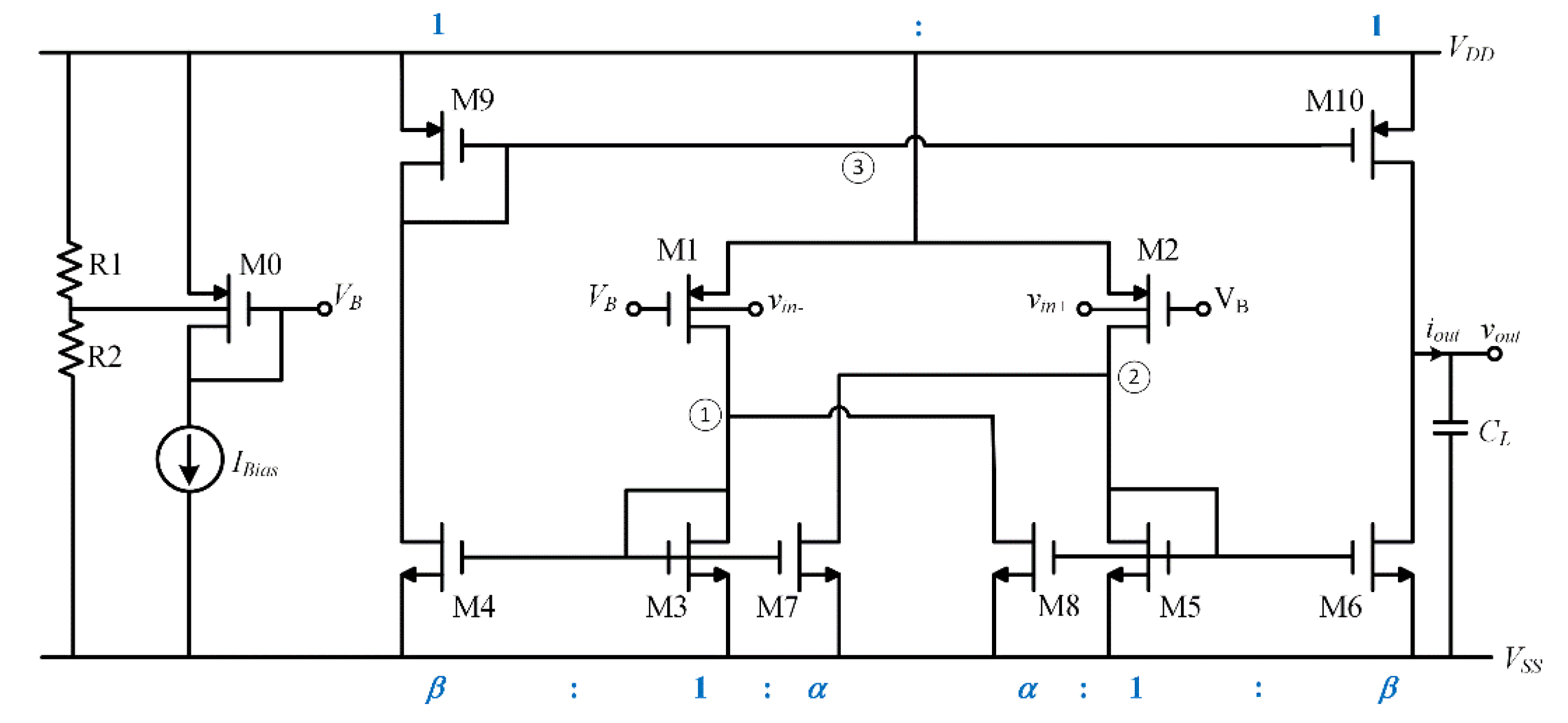
The schematic diagram of the proposed single-stage OTA is shown in Figure 1. Where not explicitly drawn, the bulk terminal of each transistor is assumed to be connected to its source. The circuit is made up of the bulk-driven non-tailed differential pair M1–M2 loaded by current mirror M3–M4 and M5–M6. The additional current mirror M9–M10 implements differential to single-ended conversion. The bias current in M1 and M2 is set through the diode-connected transistor M0, which generates voltage VB to be applied to the gates of M1–M2. The bulk terminal of M0 is biased by the voltage divider R1–R2, which is basically the analog ground i.e., the quiescent input voltage of the pair. More specifically, M0 and M1 (M2) act as a current mirror provided that Vin− = Vin+ = (R1VSS + R2VDD)/(R1 + R2), and in this case we get ID1,2 = IBias(W/L)1,2/(W/L)0.
Like the solution proposed in [12,36], an additional cross-coupled load made up of transistors M7 and M8 is exploited to produce a local positive feedback that boosts the equivalent differential transconductance, Gm. Indeed, assuming (W/L)9 = (W/L)10, i.e., unitary current mirror M9–M10, and defining parameters α and β as
and
straightforward small-signal analysis gives
where gmb1,2 is the bulk transconductance of M1 and M2.
It can be noted that, because of the absence of the tail current generator, M1–M2 is a pseudo-differential pair. However, thanks to the action of M7 and M8, the whole OTA provides a quasi-differential behavior. Indeed, Equation (3a,b) show that id3 and id5 depend on a α-weighted difference between vin+ and vin−, with ideal truly differential behavior achieved for α approaching 1.
Assuming a balanced differential input, i.e., vin+ = vd/2 and vin− = −vd/2, and no mismatches in the OTA current mirrors, the differential-mode transconductance, Gm, is found to be
where iout is the OTA short-circuit output current.
It is apparent that the differential-mode transconductance can be significantly increased by choosing suitable values of the transistor aspect ratios in (1) and (2). Of course, parameter α must be lower than 1 to ensure that the magnitude of the local positive feedback is kept below unity, to prevent the amplifier from becoming a latch. Although values very close to 1 can, in principle, generate a very large Gm increase, it is advisable to set α less than 0.9 to have a sufficient safety margin against process mismatches [34,35], while achieving a quite good differential behavior.
The complete OTA open loop transfer function, taking into account the parasitic capacitances and capacitive load, is expressed by
where ro is the OTA output resistance equal to rd10//rd6, is the sum of the load capacitance and the parasitic capacitances and Ci, I = 1, 2, 3, represents the total parasitic capacitance at nodes 1, 2 and 3. Assuming CL is much higher than the parasitic capacitances, the high-frequency poles and zeros can be neglected and the rightmost approximation in (5) holds. As usual, the gain-bandwidth product is therefore given by
From Equation (3a,b) we can also evaluate the OTA transconductance under common-mode input signal (i.e., vin+ = vin− = vcm). Ideally, in this case, the symmetry of the topology would nullify the common-mode transconductance, Gm,cm, as can be easily seen if we take the difference of id3 and id5. To have a more realistic result, we should consider the mismatches between the bulk transconductances of M1 and M2 and parameter α, by defining
After some algebraic manipulations we get
where in the approximation we neglected the term in the denominator because it is much lower than 1.
It is seen that the common-mode transconductance is proportional to the sum of the relative tolerances of gmb1,2 and parameter α. Additional degradation is also caused by mismatches in the β parameter and in the current mirror gain M9–M10, here neglected for simplicity. All these errors can be relevant due to the simple current mirror topologies adopted and can be counteracted by choosing large MOSFET channel lengths and careful layout.
By taking the ratio of (4) and (8) one can evaluate the common-mode rejection ratio (CMRR) which, as a result, is exclusively dependent on the last factor between brackets in (8).
3. Results and Comparison
The circuit in Figure 1 was designed and fabricated using a standard 180-nm CMOS process supplied by STMicroelectronics. Note that like all the recent sub-350-nm processes, the adopted technology allows the use of triple-well NMOS transistors, thus allowing independent control of the bulk terminals. The circuit layout and the chip microphotograph are shown in Figure 2. The occupied area is 866.25 μm2.
The nominal supply voltage and bias current is set equal to 400 mV and 5 nA, respectively, forcing all the transistors to work in the subthreshold region. The total nominal DC current consumption is equal to 81.35 nA. Note that with such value of VDD the potential forward biasing of the bulk-source pn junction is inherently avoided.
According to the adopted transistor dimensions summarized in Table 1, parameters α and β are nominally equal to 0.83 and 15, respectively. Consequently, the bulk transconductance of M1 and M2, equal to 4.71 μA/V, is boosted by about 88 times, yielding from (6) a theoretical GBW equal to about 5 kHz for a nominal load capacitance of 150 pF.
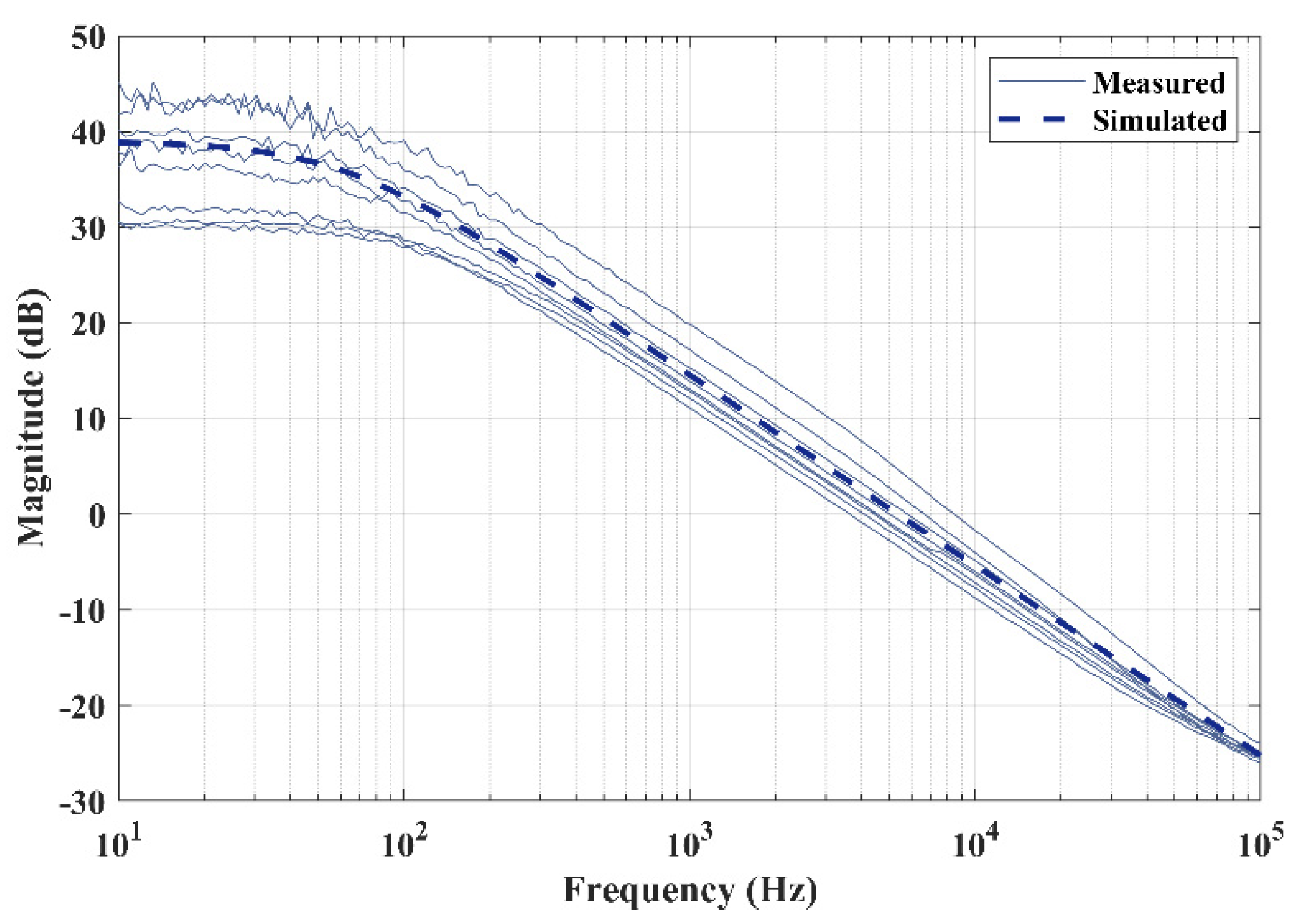
The measured open-loop Bode plots (magnitude and phase) of a representative OTA sample is depicted in Figure 3 while Figure 4 shows the measured gain for all the samples superimposed to the simulated one. Table 2 summarizes the measured main performance metrics averaged over the ten samples. The variability of the parameters is evaluated through the relative standard deviation which is lower than about 30% in all cases.
Figure 5 shows the transient response of the same sample in unity-gain feedback configuration for CL equal to 30 pF (loading capacitance equal to 30 pF represents the total load due to the package, the oscilloscope probe, and the PCB), 150 pF and 1 nF, confirming that the approximated single-pole transfer function in (5) well describes the OTA behavior.
The robustness of the OTA over process, temperature and mismatch variations is assessed through corner simulations and Monte Carlo analysis. Results are summarized in Table 3, Table 4, Table 5 and Table 6 where the main amplifier specifications are simulated over three different temperatures (namely −10 °C, 27 °C and 85 °C) in all transistor corners, showing that the amplifier is stable in all conditions. Moreover, Monte Carlo simulation results over 100 runs confirm the robustness of the OTA, the relative standard deviation being lower than 25% in all cases.
Finally, the robustness over supply voltage variations is assessed in Figure 6 where the simulated step response in unity-gain configuration is reported for different capacitive load conditions and ±10% voltage variations.
Table 6 compares the proposed OTA with other experimentally tested solutions in the literature working with a supply voltage lower than 1 V. In order to assess the trade-off between speed performance and total bias current, IT, (and, indirectly, power consumption) for a given load, we adopt in Table 3 the traditional figures of merit.
where SR is the average slew rate. To take into account also the area occupation, two additional figures of merit are adopted:
It is apparent that the proposed solution exhibits the best small-signal performance with a 4.77 X and 17.28 X improvement of IFOMS and IFOMAS over the best solutions in Table 3. Similar conclusions apply to the large-signal performance, where the improvement of IFOML and IFOMAL is equal to 2.16 X and 24.49 X. Note, however, that the gain of the proposed solution is the lowest one, being a single-stage OTA.
4. Conclusions
In this paper a power efficient single-stage, fully-differential bulk-driven OTA is introduced. The circuit is particularly suited for ultra-low-voltage applications since a novel circuit technique allows eliminating the tail current generator. Nano-power and very-low-voltage features enable operation of battery-less sensor nodes directly powered by single solar cells or operating with scaled voltage to reduce the power consumption of the digital subsection. The proposed single-stage can be profitably exploited also for the implementation of multi-stage OTAs using simple additional common-source stages to increase the total gain.
Author Contributions
Conceptualization, A.D.G.; methodology, A.D.G. and S.P.; A.D.G. and S.P.; data curation, A.B. and A.D.G.; writing—original draft preparation, A.D.G.; writing—review and editing, A.D.G. and S.P.; visualization, A.B.; supervision, A.D.G. and S.P. All authors have read and agreed to the published version of the manuscript.
Funding
Partially funded by Unict under the project PIACERI.
Conflicts of Interest
The authors declare no conflict of interest.
References
- Richelli, A.; Colalongo, L.; Kovacs-Vajna, Z.; Calvetti, G.; Ferrari, D.; Finanzini, M.; Pinetti, S.; Prevosti, E.; Savoldelli, J.; Scarlassara, S. A Survey of Low Voltage and Low Power Amplifier Topologies. J. Low Power Electron. Appl. 2018, 8, 22. [Google Scholar] [CrossRef]
- Grasso, A.D.; Pennisi, S. Ultra-Low Power Amplifiers for IoT Nodes. In Proceedings of the 2018 25th IEEE International Conference on Electronics, Circuits and Systems (ICECS), Bordeaux, France, 9–12 December 2018; pp. 497–500. [Google Scholar]
- Enabling the Internet of Things: From Integrated Circuits to Integrated Systems; Alioto, M. (Ed.) Springer International Publishing: Cham, Switzerland, 2017; ISBN 978-3-319-51480-2. [Google Scholar]
- Sansen, W. 1.3 Analog CMOS from 5 Micrometer to 5 Nanometer. In Proceedings of the 2015 IEEE International Solid-State Circuits Conference—(ISSCC) Digest of Technical Papers, San Francisco, CA, USA, 22–26 February 2015; pp. 1–6. [Google Scholar]
- Baschirotto, A.; Chironi, V.; Cocciolo, G.; D’Amico, S.; De Matteis, M.; Delizia, P. Low Power Analog Design in Scaled Technologies. Proc. Top. Workshop Electron. Part. Phys. 2009, 103–110. [Google Scholar]
- Calhoun, B.H.; Daly, D.C.; Verma, N.; Finchelstein, D.F.; Wentzloff, D.D.; Wang, A.; Cho, S.; Chandrakasan, A.P. Design Considerations for Ultra-Low Energy Wireless Microsensor Nodes. IEEE Trans. Comput. 2005, 54, 727–740. [Google Scholar] [CrossRef]
- Blalock, B.J.; Allen, P.E.; Rincon-Mora, G. Designing 1-V Op Amps Using Standard Digital CMOS Technology. IEEE Trans. Circuits Syst. II Analog. Digit. Signal Process. 1998, 45, 769–780. [Google Scholar] [CrossRef]
- Grasso, A.D.; Monsurrò, P.; Pennisi, S.; Scotti, G.; Trifiletti, A. Analysis and Implementation of a Minimum-Supply Body-Biased CMOS Differential Amplifier Cell. Very Large Scale Integr. Syst. IEEE Trans. 2009, 17, 172–180. [Google Scholar] [CrossRef]
- Monsurró, P.; Pennisi, S.; Scotti, G.; Trifiletti, A. Exploiting the Body of MOS Devices for High Performance Analog Design. IEEE Circuits Syst. Mag. 2011, 11, 8–23. [Google Scholar] [CrossRef]
- Raikos, G.; Vlassis, S. Low-Voltage Bulk-Driven Input Stage with Improved Transconductance. Int. J. Circuit Theory Appl. 2011, 39, 327–339. [Google Scholar] [CrossRef]
- Cabrera-Bernal, E.; Pennisi, S.; Grasso, A.D.; Torralba, A.; Carvajal, R.G. 0.7-V Three-Stage Class-AB CMOS Operational Transconductance Amplifier. IEEE Trans. Circuits Syst. I Regul. Pap. 2016, 63, 1807–1815. [Google Scholar] [CrossRef]
- Carrillo, J.M.; Torelli, G.; Perez-Aloe Valverde, R.; Duque-Carrillo, J.F. 1-V Rail-to-Rail CMOS OpAmp with Improved Bulk-Driven Input Stage. IEEE J. Solid-State Circuits 2007, 42, 508–517. [Google Scholar] [CrossRef]
- Zuo, L.; Islam, S.K. Low-Voltage Bulk-Driven Operational Amplifier with Improved Transconductance. IEEE Trans. Circuits Syst. I Regul. Pap. 2013, 60, 2084–2091. [Google Scholar] [CrossRef]
- Sanchotene Silva, R.; Rodovalho, L.H.; Aiello, O.; Ramos Rodrigues, C. A 1.9 NW, Sub-1 V, 542 PA/V Linear Bulk-Driven OTA with 154 DB CMRR for Bio-Sensing Applications. J. Low Power Electron. Appl. 2021, 11, 40. [Google Scholar] [CrossRef]
- Vittoz, E.; Fellrath, J. CMOS Analog Integrated Circuits Based on Weak Inversion Operations. IEEE J. Solid-State Circuits 1977, 12, 224–231. [Google Scholar] [CrossRef]
- Stockstad, T.; Yoshizawa, H. A 0.9-V 0.5-Um Rail-to-Rail CMOS Operational Amplifier. IEEE J. Solid-State Circuits 2002, 37, 286–292. [Google Scholar] [CrossRef]
- Harrison, R.R.; Charles, C. A Low-Power Low-Noise CMOS Amplifier for Neural Recording Applications. IEEE J. Solid-State Circuits 2003, 38, 958–965. [Google Scholar] [CrossRef]
- Chatterjee, S.; Tsividis, Y.; Kinget, P. 0.5-V Analog Circuit Techniques and Their Application in OTA and Filter Design. IEEE J. Solid-State Circuits 2005, 40, 2373–2387. [Google Scholar] [CrossRef]
- Valero Bernal, M.R.; Celma, S.; Medrano, N.; Calvo, B. An Ultralow-Power Low-Voltage Class-AB Fully Differential OpAmp for Long-Life Autonomous Portable Equipment. IEEE Trans. Circuits Syst. II Express Briefs 2012, 59, 643–647. [Google Scholar] [CrossRef]
- Magnelli, L.; Amoroso, F.A.; Crupi, F.; Cappuccino, G.; Iannaccone, G. Design of a 75-NW, 0.5-V Subthreshold Complementary Metal–Oxide–Semiconductor Operational Amplifier. Int. J. Circuit Theory Appl. 2014, 42, 967–977. [Google Scholar] [CrossRef]
- Grasso, A.D.; Marano, D.; Palumbo, G.; Pennisi, S. Design Methodology of Subthreshold Three-Stage CMOS OTAs Suitable for Ultra-Low-Power Low-Area and High Driving Capability. IEEE Trans. Circuits Syst. I Regul. Pap. 2015, 62, 1453–1462. [Google Scholar] [CrossRef]
- Qin, Z.; Tanaka, A.; Takaya, N.; Yoshizawa, H. 0.5-V 70-NW Rail-to-Rail Operational Amplifier Using a Cross-Coupled Output Stage. IEEE Trans. Circuits Syst. II Express Briefs 2016, 63, 1009–1013. [Google Scholar] [CrossRef]
- Lehmann, T.; Cassia, M. 1-V Power Supply CMOS Cascode Amplifier. IEEE J. Solid-State Circuits 2001, 36, 1082–1086. [Google Scholar] [CrossRef]
- Ferreira, L.H.C.; Pimenta, T.C.; Moreno, R.L. An Ultra-Low-Voltage Ultra-Low-Power CMOS Miller OTA with Rail-to-Rail Input/Output Swing. IEEE Trans. Circuits Syst. II Express Briefs 2007, 54, 843–847. [Google Scholar] [CrossRef]
- Ferreira, L.H.C.; Sonkusale, S.R. A 60-DB Gain OTA Operating at 0.25-V Power Supply in 130-Nm Digital CMOS Process. IEEE Trans. Circuits Syst. I Regul. Pap. 2014, 61, 1609–1617. [Google Scholar] [CrossRef]
- Colletta, G.D.; Ferreira, L.H.C.; Pimenta, T.C. A 0.25-V 22-NS Symmetrical Bulk-Driven OTA for Low-Frequency Gm-C Applications in 130-Nm Digital CMOS Process. Analog. Integr. Circuits Signal Process. 2014, 81, 377–383. [Google Scholar] [CrossRef]
- Abdelfattah, O.; Roberts, G.W.; Shih, I.; Shih, Y.C. An Ultra-Low-Voltage CMOS Process-Insensitive Self-Biased OTA with Rail-to-Rail Input Range. IEEE Trans. Circuits Syst. I Regul. Pap. 2015, 62, 2380–2390. [Google Scholar] [CrossRef]
- Kulej, T.; Khateb, F. Design and Implementation of Sub 0.5-V OTAs in 0.18-μm CMOS. Int. J. Circuit Theory Appl. 2018, 46, 1129–1143. [Google Scholar] [CrossRef]
- Kulej, T.; Khateb, F. A 0.3-V 98-DB Rail-to-Rail OTA in 0.18 μm CMOS. IEEE Access 2020, 8, 27459–27467. [Google Scholar] [CrossRef]
- Kulej, T.; Khateb, F. A Compact 0.3-V Class AB Bulk-Driven OTA. IEEE Trans. Very Large Scale Integr. Syst. 2020, 28, 224–232. [Google Scholar] [CrossRef]
- Woo, K.-C.; Yang, B.-D. A 0.25-V Rail-to-Rail Three-Stage OTA with an Enhanced DC Gain. IEEE Trans. Circuits Syst. II Express Briefs 2020, 67, 1179–1183. [Google Scholar] [CrossRef]
- Centurelli, F.; Della Sala, R.; Monsurrò, P.; Scotti, G.; Trifiletti, A. A 0.3 V Rail-to-Rail Ultra-Low-Power OTA with Improved Bandwidth and Slew Rate. J. Low Power Electron. Appl. 2021, 11, 19. [Google Scholar] [CrossRef]
- Centurelli, F.; Della Sala, R.; Scotti, G.; Trifiletti, A. A 0.3 V, Rail-to-Rail, Ultralow-Power, Non-Tailed, Body-Driven, Sub-Threshold Amplifier. Appl. Sci. 2021, 11, 2528. [Google Scholar] [CrossRef]
- Ballo, A.; Grasso, A.D.; Pennisi, S. Active Load with Cross-Coupled Bulk for High-Gain High-CMRR Nanometer CMOS Differential Stages. Int. J. Circuit Theory Appl. 2019, 47, 1700–1704. [Google Scholar] [CrossRef]
- Wang, R.; Harjani, R. Partial Positive Feedback for Gain Enhancement of Low-Power CMOS Otas. Analog. Integr. Circuits Signal Processing 1995, 8, 21–35. [Google Scholar] [CrossRef]
- Roh, J.; Byun, S.; Choi, Y.; Roh, H.; Kim, Y.-G.; Kwon, J.-K. A 0.9-V 60-mW 1-Bit Fourth-Order Delta-Sigma Modulator with 83-DB Dynamic Range. IEEE J. Solid-State Circuits 2008, 43, 361–370. [Google Scholar] [CrossRef]
Figure 1.
Proposed single-stage OTA.

Figure 2.
Layout and chip microphotograph of the proposed OTA.

Figure 3.
Measured open-loop AC response for CL = 150 pF.

Figure 4.
Measured open-loop gain for all the samples superimposed to simulations for CL = 150 pF.

Figure 5.
Measured step response in unity gain configuration for different capacitive loads.

Figure 6.
Simulated transient response for supply voltage variations of ±10% for: (a) CL = 30 pF, (b) CL = 150 pF and (c) CL = 1 nF.
Figure 6.
Simulated transient response for supply voltage variations of ±10% for: (a) CL = 30 pF, (b) CL = 150 pF and (c) CL = 1 nF.


Table 1.
Transistor dimensions.
| Device | Value (µm/µm) |
|---|---|
| M0, M1, M2 | 3/0.26 (×2) |
| M3, M5 | 6/0.26 |
| M4, M6 | 6/0.26 (×15) |
| M7, M8 | 5/0.26 |
| M9, M10 | 6/0.26 (×4) |
Table 2.
Average main performance parameters over 10 samples for CL = 150 pF.
| Parameter | Average | Min | Max |
|---|---|---|---|
| DC Gain (dB) | 37.7 | 30.1 | 45.2 |
| GBW (kHz) | 5.56 | 3.64 | 8.84 |
| Phase Margin (deg) | 79.3 | 66.9 | 87.5 |
| Positive Slew Rate (V/ms) | 7.43 | 6.34 | 8.52 |
| Negative Slew Rate (V/ms) | 7.36 | 6.28 | 8.74 |
Table 3.
Corner and Monte Carlo analysis results for T = −10 °C.
| Parameter | TT | SS | SF | FS | FF | Monte Carlo | |
|---|---|---|---|---|---|---|---|
| µ | σ | ||||||
| Power (nW) | 26.1 | 19 | 18.3 | 20.5 | 29.8 | 24 | 4.6 |
| DC Gain (dB) | 34.1 | 23.6 | 20.4 | 43.6 | 41.7 | 33 | 9.7 |
| GBW (kHz) | 1.51 | 0.39 | 0.25 | 3.56 | 4.13 | 1.94 | 0.48 |
| Phase Margin (deg) | 88.9 | 93.2 | 94.7 | 77.6 | 77.8 | 86.1 | 14.3 |
| Positive Slew Rate (V/ms) | 7.37 | 8.07 | 7.85 | 6.8 | 6.6 | 7.33 | 0.47 |
| Negative Slew Rate (V/ms) | 7.32 | 8.04 | 7.82 | 6.78 | 6.6 | 7.29 | 0.46 |
Table 4.
Corner and Monte Carlo analysis results for T = 27 °C.
| Parameter | TT | SS | SF | FS | FF | Monte Carlo | |
|---|---|---|---|---|---|---|---|
| µ | σ | ||||||
| Power (nW) | 32.5 | 30.9 | 31.6 | 32.1 | 33.6 | 32.4 | 2.6 |
| DC Gain (dB) | 44.6 | 42.3 | 40 | 45.7 | 45.2 | 44.4 | 5.7 |
| GBW (kHz) | 5.66 | 4.06 | 3.3 | 6.32 | 6.42 | 5.75 | 1.12 |
| Phase Margin (deg) | 66.2 | 75.5 | 80 | 62.9 | 62.7 | 67.9 | 15.1 |
| Positive Slew Rate (V/ms) | 7.45 | 8.23 | 8.01 | 6.89 | 6.65 | 7.43 | 0.48 |
| Negative Slew Rate (V/ms) | 7.37 | 8.14 | 7.92 | 6.85 | 6.6 | 7.36 | 0.47 |
Table 5.
Corner and Monte Carlo analysis results for T = 85 °C.
| Parameter | TT | SS | SF | FS | FF | Monte Carlo | |
|---|---|---|---|---|---|---|---|
| µ | σ | ||||||
| Power (nW) | 36.6 | 35.6 | 37 | 36.5 | 37.8 | 36.8 | 2.4 |
| DC Gain (dB) | 44.7 | 45.1 | 44.2 | 44.8 | 44.2 | 45 | 4.9 |
| GBW (kHz) | 5.94 | 5.87 | 5.71 | 6.02 | 5.94 | 6.28 | 1.48 |
| Phase Margin (deg) | 61.4 | 60.8 | 62.1 | 62.1 | 62.7 | 64.2 | 17.6 |
| Positive Slew Rate (V/ms) | 7.53 | 8.33 | 8.15 | 6.96 | 6.74 | 7.51 | 0.49 |
| Negative Slew Rate (V/ms) | 7.44 | 8.23 | 8.01 | 6.91 | 6.66 | 7.43 | 0.47 |
Table 6.
Comparison With Other Sub-1-V OTAs.
| Ref. # | [7] | [18] | [24] | [12] | [10] | [19] | [13] | [25] | [20] | [27] | [22] | [11] | [28] | [30] | [29] | [31] | This Work |
|---|---|---|---|---|---|---|---|---|---|---|---|---|---|---|---|---|---|
| Year | 1998 | 2005 | 2007 | 2007 | 2011 | 2012 | 2013 | 2014 | 2014 | 2015 | 2016 | 2016 | 2018 | 2020 | 2020 | 2020 | 2022 |
| Technology [μm] | 2 | 0.18 | 0.35 | 0.35 | 0.18 | 0.18 | 0.35 | 0.13 | 0.18 | 0.065 | 0.18 | 0.18 | 0.18 | 0.18 | 0.18 | 0.065 | 0.18 |
| Area [mm2] | 1.515 | 17 | 0.06 | 0.0532 | 0.063 | 0.057 | 0.1575 | 0.083 | 0.057 | 0.00495 | 0.036 | 0.0198 | 0.0082 | 0.0085 | 0.0098 | 0.002 | 8.66 × 10⁻⁴ |
| Supply [V] | 1 | 0.5 | 0.6 | 1 | 1 | 0.8 | 1 | 0.25 | 0.5 | 0.5 | 0.5 | 0.7 | 0.3 | 0.3 | 0.3 | 0.25 | 0.4 |
| CL [pF] | 22 | 20 | 15 | 17 | 1 | 8 | 15 | 15 | 30 | 3 | 40 | 20 | 20 | 30 | 30 | 15 | 150 |
| DC gain [dB] | 49 | 62 | 69 | 76.2 | 64 | 51 | 88 | 60 | 70 | 46 | 77 | 57 | 63 | 65 | 98.1 | 70 | 38 |
| Ibias [μA] | 300 | 150 | 0.9 | 358 | 130 | 1.5 | 197 | 0.072 | 0.15 | 366 | 0.14 | 36 | 0.056 | 0.042 | 0.04333 | 0.10400 | 0.08135 |
| Power [μW] | 300 | 75 | 0.54 | 358 | 130 | 1.2 | 197 | 0.018 | 0.075 | 183 | 0.07 | 25.2 | 0.0168 | 0.0126 | 0.013 | 0.026 | 0.03254 |
| GBW [MHz] | 1.3 | 10 | 0.011 | 8.1 | 2 | 0.057 | 11.67 | 0.002 | 0.018 | 38 | 0.004 | 3 | 0.0028 | 0.00296 | 0.0031 | 0.0095 | 0.00556 |
| PM [°] | 57 | 60 | 65 | 45 | 60 | 66 | 53 | 55 | 57 | 56 | 60 | 61 | 52 | 54 | 88 | 79 | |
| SR [V/μs] a | 1.6 | 2 | 0.015 | 3.88 | 0.7 | 0.14 | 1.95 | 0.0007 | 0.003 | 43 | 0.002 | 2.8 | 0.0071 | 0.00415 | 0.0091 | 0.002 | 0.0074 |
| CMRR [dB] | 56.2 | 65 | 74.5 | 70.5 | 88 | 65 | 40 | - | - | 35 | 55 | 19 | 72 | 110 | 60 | 62.5 | 36 |
| PSRR [dB] | 60.8 | 43 | - | 45 | 70 | - | 40 | - | - | 37 | 52 | 52 | 62 | 56 | 61 | 38 | 30 |
| Operation mode | BD | GD | BD | BD | BD | GD | BD | BD | GD | BD | GD | BD | BD | BD | BD | BD | BD |
| Stage # | 2 | 2 | 2 | 1 | 2 | 1 | 2 | 2 | 2 | 3 | 2 | 3 | 2 | 2 | 3 | 3 | 1 |
| IFOMS [MHz⋅pF/μA] | 0.10 | 1.33 | 0.18 | 0.38 | 0.02 | 0.30 | 0.89 | 0.42 | 3.60 | 0.31 | 1.14 | 1.67 | 1.00 | 2.11 | 2.15 | 1.37 | 10.25 |
| IFOML [(V/μs)⋅pF/μA] | 0.12 | 0.27 | 0.25 | 0.18 | 0.01 | 0.75 | 0.15 | 0.15 | 0.60 | 0.35 | 0.57 | 1.56 | 2.54 | 2.96 | 6.30 | 0.29 | 13.64 |
| IFOMAS [MHz⋅pF/μA⋅mm2] | 0.06 | 78.43 | 3.06 | 7.23 | 0.24 | 5.33 | 5.64 | 5.02 | 63.16 | 62.92 | 31.75 | 84.18 | 121.95 | 248.74 | 219.00 | 685.10 | 11,838.33 |
| IFOMAL [(V/μs)⋅pF/μA⋅mm2] | 0.08 | 15.69 | 4.17 | 3.46 | 0.09 | 13.10 | 0.94 | 1.76 | 10.53 | 71.20 | 15.87 | 78.56 | 309.23 | 348.74 | 642.86 | 144.23 | 15,745.41 |
a average value.
Publisher’s Note: MDPI stays neutral with regard to jurisdictional claims in published maps and institutional affiliations. |
© 2022 by the authors. Licensee MDPI, Basel, Switzerland. This article is an open access article distributed under the terms and conditions of the Creative Commons Attribution (CC BY) license (https://creativecommons.org/licenses/by/4.0/).
Share and Cite
MDPI and ACS Style
Ballo, A.; Grasso, A.D.; Pennisi, S. 0.4-V, 81.3-nA Bulk-Driven Single-Stage CMOS OTA with Enhanced Transconductance. Electronics 2022, 11, 2704. https://0-doi-org.brum.beds.ac.uk/10.3390/electronics11172704
AMA Style
Ballo A, Grasso AD, Pennisi S. 0.4-V, 81.3-nA Bulk-Driven Single-Stage CMOS OTA with Enhanced Transconductance. Electronics. 2022; 11(17):2704. https://0-doi-org.brum.beds.ac.uk/10.3390/electronics11172704
Chicago/Turabian StyleBallo, Andrea, Alfio Dario Grasso, and Salvatore Pennisi. 2022. "0.4-V, 81.3-nA Bulk-Driven Single-Stage CMOS OTA with Enhanced Transconductance" Electronics 11, no. 17: 2704. https://0-doi-org.brum.beds.ac.uk/10.3390/electronics11172704
Note that from the first issue of 2016, this journal uses article numbers instead of page numbers. See further details here.