
A Novel Ring-Gate AlGaN/GaN HEMT Device and Electrode Structure Optimization
by
Yanxu Zhu
1, 
Xiaomeng Song
1,*,
Jianwei Li
2,
Jinheng Li
1,
Baoliang Fei
1,
Peiyang Li
1 and
Fajun Li
3,* 1
Key Laboratory of Photoelectron Technology Ministry of Education, Beijing University of Technology, Beijing 100124, China
2
Chipone Technology (Beijing) Company Limited, Beijing 100176, China
3
The National Astronomical Observatory of China, Beijing 100101, China
*
Authors to whom correspondence should be addressed.
Electronics 2022, 11(20), 3329; https://0-doi-org.brum.beds.ac.uk/10.3390/electronics11203329
Submission received: 13 September 2022
/
Revised: 11 October 2022
/
Accepted: 12 October 2022
/
Published: 16 October 2022
(This article belongs to the Topic Advances in Microelectronics and Semiconductor Engineering)
Abstract
:In this paper, a novel ring-gate structure AlGaN/GaN HEMT device is proposed and fabricated successfully. When the gate-source spacing Lgs = 5 μm, gate-drain spacing Lgd = 7 μm, gate length Lg = 3 μm, the maximum drain current Idmax of this ring-gate AlGaN/GaN HEMT device improved by 161.8% comparing with the conventional structure device, the threshold voltage Vth increased by 66.7% from 1.65 V to 2.5 V. In order to further improve the performance of the device, a series of electrode structure optimization designs have been carried out. Firstly, the effect of source-drain electrode alloy type and etching depth under source-drain region on the transfer and output characteristics was investigated, we fabricated devices with two alloy electrodes of multi-layer Ti/Al/Ti/Al/Ti/Al/Ni/Au and single layer Ti/Al/Ni/Au, then perform groove etching under the source and drain electrodes, the etching depth is set to 10/20 nm, after analysis and calculation, it is found that among ring-gate and conventional-gate devices, the device with multi-layer electrodes and an etched depth of 10 nm performs best. Then, the influence of device size parameters on transfer and output characteristics was explored, devices with different Lg and Lgd were prepared, after testing it is found that with the increase of Lg, the Vth of the conventional-gate and ring-gate HEMT devices both showed a positive-shift trend, in conventional device Vth increased from 1.53 V to 1.7 V, and this value increased from 1.5 V to 2.5 V in ring-gate device; the saturation drain current decreases when Lg increasing, and the decrease of the ring-gate device is more obvious, from 51.28 mA at Lg = 3 μm to 24.48 mA at Lg = 6 μm; when Lds decreases, the Vth of the two structures doesn’t change significantly, but the output current increases with the reduction of Lds, among them, the Idmax of the conventional structure device at Lgd = 19 um is 79.07% lower than that at Lgd = 7 μm; the value of the ring-gate device is reduced by 113.7%. In addition, among all the above devices, the ring-gate devices all show better output characteristics and higher Vth than conventional devices.
1. Introduction
AlGaN/GaN HEMTs are widely used in high-voltage and high-frequency power devices and switching devices due to their high electron mobility, high breakdown electric field, and high saturation current [1,2]. AlGaN/GaN heterojunction is the core of AlGaN/GaN HEMT devices, when the semiconductor material GaN is combined with the ternary alloy AlGaN, strong spontaneous and piezoelectric polarization effects will occur at the interface of the heterojunction, generating 2-dimensional electron gas(2DEG) with high concentration and mobility, and form the conductive channel of AlGaN/GaN HEMTs. By controlling the gate voltage, the concentration of 2DEG can be adjusted, which is how AlGaN/GaN HEMTs work.
In the practical application of AlGaN/GaN HEMTs, considering the safety of the circuit system, the complexity of the circuit design, and the electrical performance of the device, enhancement-mode devices with positive threshold voltage gradually take the lead, good transfer and output characteristics also become essential evaluation indicators for devices. At present, many researchers have improved the above characteristics by optimizing the structure and materials of GaN HEMTs [3,4,5]. In 2000, Zhang N Q of UCSB improved the electric field distribution at the gate edge by using a gate field plate structure, the breakdown voltage of his device is increased by 170 V [6]. In 2011, LEE et al. improved the gold-free ohmic contact characteristics by changing the groove etching depth below the electrode [7]. In 2016, Zhou Q et al. adopted the trench gate and MIS gate structure, succesfully improved the threshold voltage and output current density [8]. In 2019, Zhao S L et al. prepared a circular AlGaN/GaN/AlGaN double heterojunction HEMT, the edge effect is greatly reduced, the output and breakdown characteristics are improved significantly [9]. In 2021, WEI X innovatively proposed a laterally coupled P-GaN gate structure HEMT, its drain current increased by 87.9% with a 10 μm gate-drain spacing [10].
In recent years, the continuous development of power electronics technology has put forward higher requirements for the electrical characteristics of semiconductor electronic devices. How to achieve higher saturation current, higher output power and better turn-on characteristics on the premise of ensuring circuit safety and low cost is still the focus of current research. Target at the questions above, in this paper, a series of optimized designs for the gate shape and electrode structure of AlGaN/GaN HEMTs were carried out, a novel ring-gate structure HEMT was proposed and successfully fabricated, meanwhile the conventional strip-gate structure HEMT was prepared as a comparison. By optimizing the electrode structure and size parameters, the effects on the transfer and output characteristics of the device were explored. Finally, the optimal performance of the device was obtained with the multi-layer Ti/Al/Ti/Al/Ti/Al/Ni/Au electrodes and 10 nm groove etching under the source and drain, when the Lg = 3 μm, the Lgd = 7 μm. Compared with the conventional structure device under the same conditions, the output current is increased by 68.07%. Which has positive significance for further improving the electrical properties of AlGaN/GaN HEMT devices.
2. Materials and Methods
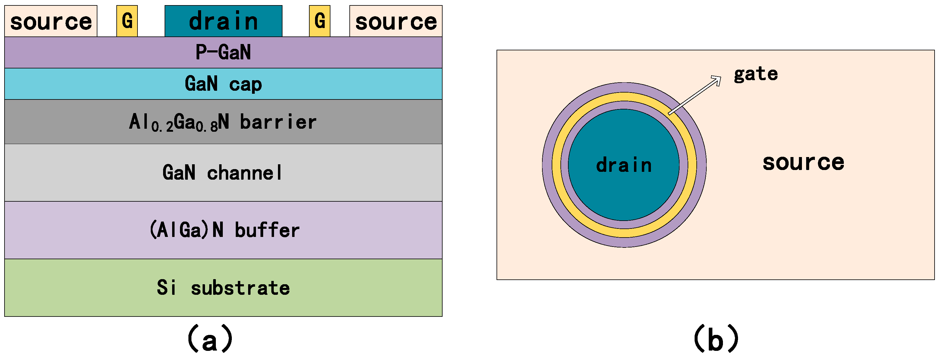
In this experiment, we use the AlGaN/GaN HEMT epitaxial wafer manufactured by Shanghai Gadan Electronic Information Company. This epitaxial are consist of a 100 nm thick P-GaN cap layer, a 2 nm GaN cap layer, a 13 nm Al0.27Ga0.73N barrier layer, a 300 nm GaN channel layer and AlGaN buffer layer, a Si substrate. The 2DEG concentration is 8 × 1012 cm−2, the electron mobility is measured to be about 1300 cm2/V−1s−1 after etching the P-GaN layer outside the gate.
This paper proposes a novel ring-gate structure. As shown in Figure 1, the drain portion of the device is circular, the gate is a ring surrounding the drain. We firstly prepared AlGaN/GaN HEMT devices with ring-gate structure, and also prepared conventional gate HEMT devices as a comparsion. The gate-source spacing Lgs is set to 5 μm, the gate length Lg is 3 μm, and the gate-drain spacing Lgd is 7 μm, so as to study the influence of the gate shape change on the device performance. The schematic diagram of the 3D structure of the two devices is shown in Figure 2.
In order to obtain better ohmic contact to ensure characteristics, as shown in Table 1, we set two source-drain electrode structures: Ti/Al/Ti/Al/Ti/Al/Ni/Au (5/50/5/50/5/50/40/50 nm) multi-layer electrodes and Ti/Al/Ni/Au (15/150/40/50 nm) single layer electrodes, and set two etched depth of 10 nm and 20 nm under the source and drain electrodes. Then, the influence of gate length and source-drain spacing on device performance was further optimized. We prepared 4 groups of devices with Lgs of 5 μm, Lg of 3 μm, Lgd of 7/11/15/19 μm; and 4 groups of devices with Lgs of 5 μm, Lgd of 11 μm, Lg of 3/4/5/6 μm respectively. Each group of devices includes two structures, ring-gate and conventional gate. To analyze and compare the test results more clearly and intuitively, we have grouped and named the different devices prepared, and the specific grouping of the devices is shown in Table 2, Table 3 below.
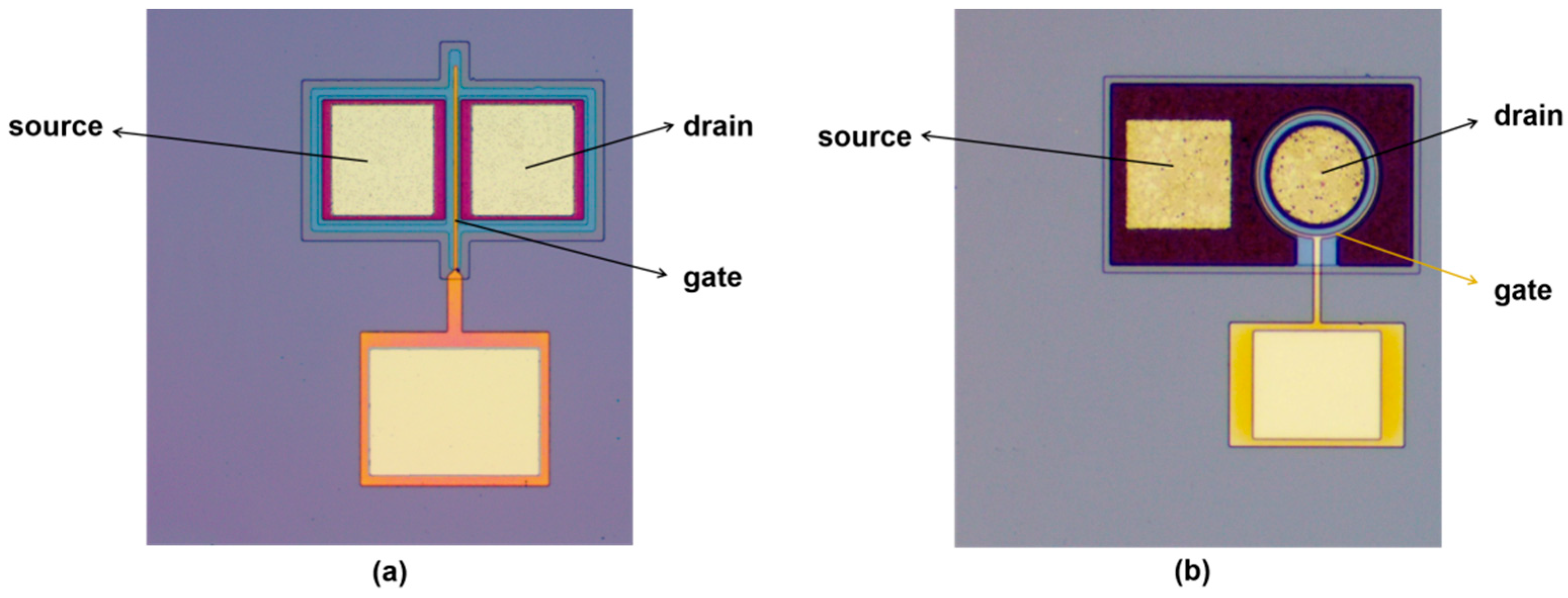
The devices prepared in this experiment are enhancement-mode AlGaN/GaN HEMT devices with P-GaN gate structure. The fabrication process of the device includes the following steps: (1) In order to prevent the fusion of 2DEG between different devices and the contact between the subsequently grown electrode metals, at first, use the photoresist as a mask, then use the inductively coupled plasma chemical vapor deposition (ICPCVD) technology to isolate the mesa between devices on the epitaxial wafer. The ICP/RF power is set to 225/225 W, the tray temperature is 30 °C, the chamber atmosphere SiCl4/Ar is 30/10 sccm, the etching time is 1 min 35 s, and the etching depth is about 370 nm. (2) Next, a layer of 200 nm thick SiO2 is deposited by plasma enhanced chemical vapor deposition (PECVD) technology, then the area outside the active area is corroded with HF, only the SiO2 in the non-active area is retained. This SiO2 layer can better prevent the flow of 2DEG between devices and ensure subsequent processes and the resulting device performance. (3) To obtain enhancement-mode devices and better ohmic contact characteristics, next use the ICP etching technology to etch the P-GaN except for the area under the gate. The etching depth is about 100 nm, and in order to precisely control the etching rate to prevent over-etching and less-etching, the ICP/RF power is adjusted to 225/35 W here, the tray temperature is 20 °C, the chamber atmosphere SiCl4/Ar is 10/3 sccm, now the etching rate can be reduced to about 1 nm/s. (4) Finally, the Discovery 635 multi-target magnetron puttering table was used for growthing the source, drain and gate electrodes, the gate metal is Ni/Au (45/200 nm) alloy, the source, drain electrodes were provided with multi-layer Ti/Al/Ti/Al/Ti/Al/Ni/Au (5/50/5/50/5/50/40/50 nm) and single layer Ti/Al/Ni/Au (15/150/40/50 nm). After sputtering, the device was placed under N2 atmosphere for rapid thermal annealing at 850 °C for 30 s to form ohmic contacts. (5) To protect the device from oxidation and suppress the current collapse, use the photoresist as a mask, 300 nm thick SiO2 was deposited as a passivation layer by ICPCVD technology. Afterwards, the passivation layer at the source, drain and gate electrodes is removed with a stripping solution to form the final device. (6) Use the B1500A to measure the transfer and output characteristic curve of the above devices. The optical microscope images of the conventional and ring-gate HEMT devices finally prepared are shown in Figure 3.
3. Results and Discussion
3.1. Influence of Gate Shape on Device Performance
After the above process steps, we firstly prepared a ring-gate AlGaN/GaN HEMT device with a Lg of 3 μm, Lgs of 5 μm, and Lgd of 7 μm. A conventional structure HEMT device with the same size parameters was prepared for comparison. Both of them use Ti/Al/Ni/Au as source-drain electrode material and Ni/Au as gate material. The transfer and output characteristics of them were tested with B1500A. Their transfer characteristic curve is shown in Figure 4a, it can be found that both devices realize the enhancement mode, but the Vth of the ring-gate device (2.75 V) is significantly higher than that of the conventional structure device (1.65 V), which is increased by 66.7%; and a current surge occurs after the conventional device is turned on, which will greatly damage the safety of the device during operation [2]. Compared with it, ring-gate devices is turned on more smoothly. Since the transfer characteristic curve shows the control ability of VGS to ID, therefore, the conclusion is that the ring gate has stronger grating control ability, which makes the HEMT device open smoothly and ensures the safety of it during operation. This is beneficial for improving circuit safety and improving system reliability. The output characteristic curves of the two devices at Vg = 4/5/6 V are shown in Figure 4b, the output current of the ring-gate AlGaN/GaN HEMT device is significantly higher than that of the conventional structure device, when Vg = 6 V, the maximum output current of the ring-gate device reaches 28.56 mA, which is obviously higher than that of the conventional device (10.91 mA) under the same conditions, with an increase of 161.8%. This indicates that the ring-shape gate greatly improves the DC characteristics of the device, this is because the effective length of the ring-gate is larger than that of the conventional strip gate, its stability is higher, and the parasitic resistance is smaller, can effectively improve device gate control capability [9]; at the same time, the ring-gate structure is connected end to end without terminal, which can suppress edge effects, makes the gate-edge electric field distribution more uniform, resulting in lower on-resistance, higher output current [9]; meawhile, the P-GaN remaining under the ring-gate is also ring-shaped, so its stability and effective length are also higher, therefore, the depletion effect on 2DEG is also more significantly, so that can better ensure the turn-on of the device, obtain a higher Vth and better transfer characteristics.
3.2. Influence of Source-Drain Electrode Material and Groove Etching on Device Performance
Optimizing the source-drain electrode structure and fabrication conditions of AlGaN/GaN HEMT devices can improve the ohmic contact characteristics, thereby improving the electrical properties of the device. We prepared 8 groups of devices as shown in Table 1, and explored the effects of electrode alloy materials and source-drain grooves etching depth on device performance. The area of the groove etching area is smaller than that of the source-drain electrode itself, as shown in Figure 5a,b, the source, drain electrodes of conventional devices are 143 × 140 μm rectangles, while the groove etching area is 120 × 130 μm rectangles; the radius of the drain of the ring-gate device is 63 μm, while the radius of the groove etched region is 58 μm, and the etched groove under the source is a square of 130 × 130 μm. The source and drain electrodes of all devices are made of Ti/Al/Ni/Au (15/150/40/50 nm) alloy, the gates are made of Ni/Au (45/200 nm) alloy, the gate length Lg is 3 μm, the gate-source spacing is 5 μm, and the gate-drain spacing is 7 μm.
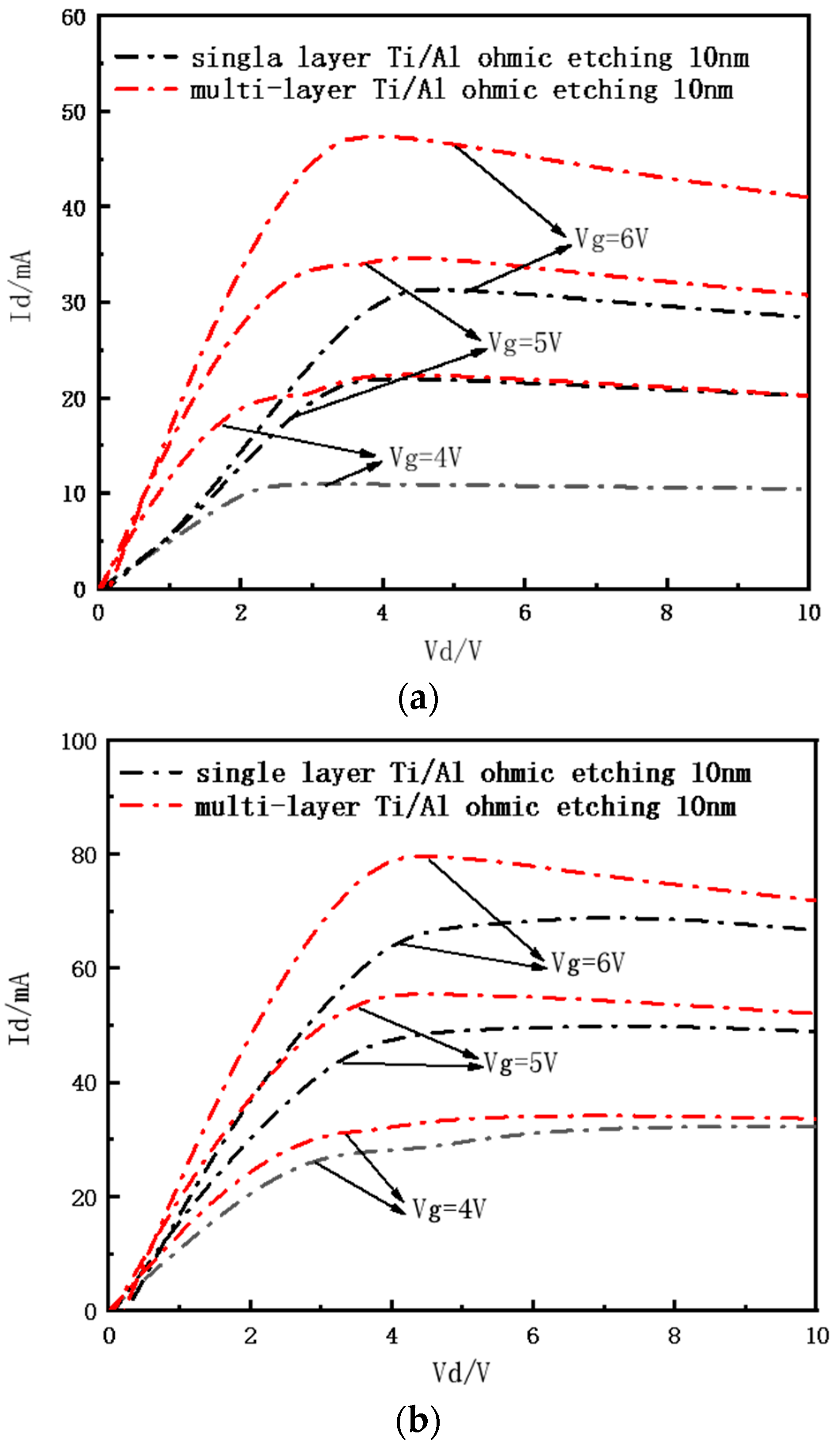
As shown in Figure 6a,b, the output characteristics of conventional and ring-gate HEMT with an ohmic etching depth of 10/20 nm are compared. It can be seen that, compared with the devices without ohmic groove etching, the devices show better output characteristics and larger output current after etching, and the output current of the device etched by 10 nm is significantly larger than that of the device etched by 20 nm. When Vg = 6 V, the maximum output current of the conventional structure device with an etching depth of 10 nm reached 31.28 mA, compared with the device etched 20 nm (19.49 mA), it is improved by 60.5%. The maximum output current of the ring-gate HEMT device etched with 10 nm reaches 68.80 mA, which is 54.4% higher than that of the 20nm etched device (44.55 mA). This is because the etched ohmic groove under the source-drain electrode increases the reaction area between the source-drain electrode metal and the underlying AlGaN barrier layer, and reduce the distance from the ohmic electrode to the 2DEG channel, thereby increasing the probability of electron tunneling between ohmic metal and the 2DEG channel [11], it is beneficial for the low-resistance TiN alloy formed after ohmic electrode annealing to diffuse into the buffer layer, and directly connect to the 2DEG channel, making the contact resistance lower, the output current higher. In addition, ICP etching also introduces some lattice defects that can establish a preferential path for current flow and therefore enhance the current through the heterojunction [11]. But correspondingly, ICP etching will also introduce some etching damage, making the electrodes rough, which increases the contact resistance and thus increases the on-resistance; when the etching depth is large, the remaining AlGaN barrier layer is too thin to support the AlGaN/GaN heterojunction to provide enough 2DEG, resulting in the decline of the output current. Therefore, a moderate groove etching depth should be selected to ensure the output characteristics of the device.
Figure 7a,b shows the output characteristic curves of conventional and ring-gate structure devices with a 10 nm ohmic groove etching using multi-layer Ti/Al and single-layer Ti/Al electrode respectively. It can be found that both devices exhibit better output characteristics with multi-layer electrodes, when Vg = 6 V, the Idmax of multi-layer conventional device comes to 47.38 mA, which is 51.3% higher than that of the single-layer device (31.32 mA); in ring-gate multi-layer electrode devices, the maximum output current reaches 79.63 mA, which is 15.7% higher than that of the single-layer electrode device (68.80 mA). This is because when the multiple Ti/Al/Ti/Al/Ti/Al/Ni/Au is subjected to rapid thermal annealing, the Al material can react with Ti more fully, which is beneficial to consume Al atoms and Ti to form low-resistance Ti-Al alloy, reducing the generation of Al-Au alloy particles, which will increase the surface roughness and the contact resistance of the electrode [11,12,13,14,15], thus can make the electrode metal after annealing more uniform and stable [11]. Therefore, the device using multiple Ti/Al electrode can obtain better ohmic contact characteristics and thus generate a larger output current.
In summary, multiple Ti/Al electrode and ohmic groove etching can effectively improve the output current, lower the on-resistance, and significantly enhance the electrical properties of the device, and the optimal ohmic groove etching depth is 10 nm. Moreover, in each group of devices above, the output current of the ring-gate structure HEMT device is significantly higher.
3.3. Influence of Electrode Size Parameters on Device Performance
3.3.1. The Effect of Gate Length on Device Performance
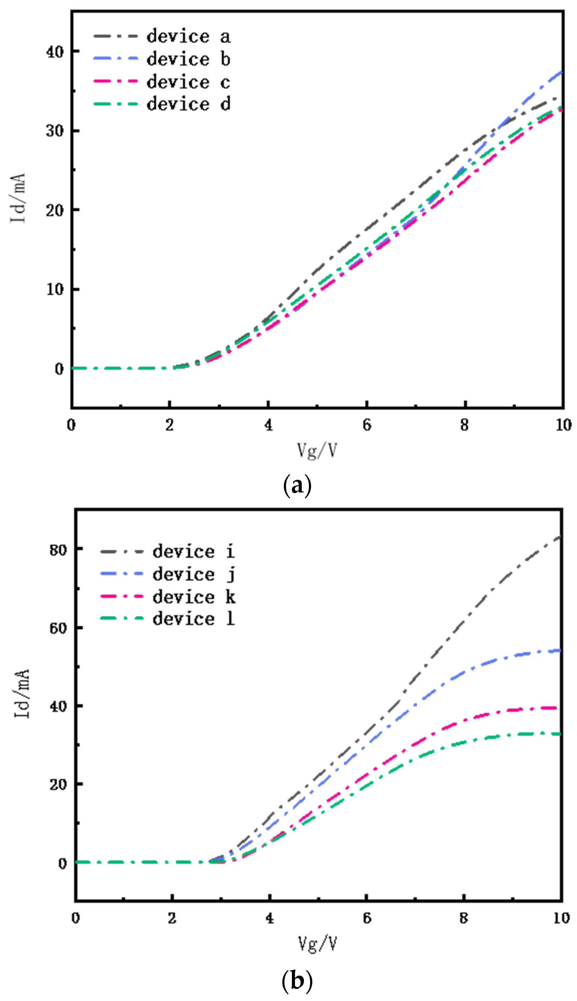
Firstly, keep the gate-drain spacing at 11 μm and the gate-source spacing at 5 μm, use Ti/Al/Ni/Au alloy as source, drain electrode meterials, and Ni/Au as gate electrode material, the etching depth under the source, drain is set to 10 nm, we fabricated conventional and ring-gate structure HEMT devices with gate lengths of 3/4/5/6 μm respectively. These devices are grouped as shown in Table 2, Table 3, the output and transfer characteristics are tested. Figure 8a shows the transfer characteristic curves of the conventional structure with Lg of 3/4/5/6 μm respectively. It can be seen that with the increase of Lg, the Vth of the device shows a positive shift trend. When Lg = 3 μm, the Vth = 1.53 V, when Lg increases to 6 μm, Vth increases to 1.7 V. In Figure 8b we can observe the same trend among the ring-gate structure devices, and the positive shift of Vth is more obvious. The Vth of device p with Lg of 6 μm is about 2.5 V, while the Vth of device m with Lg of 3 μm is only about 1.5 V.
When Vg = 6 V, the output characteristics of conventional and ring-gate HEMT devices with Lg of 3/4/5/6 μm are shown in Figure 9a,b. It can be seen that when Lg of the device increases sequentially, its saturation drain current decreases instead. In conventional structure devices, the Idmax when Lg = 3 μm is 17.77 mA, when Lg = 6 μm, the saturation current is reduced to 16.21 mA, in ring-gate devices, the saturation current decreases more significantly, from 51.28 mA when Lg = 3 μm to 24.48 mA when Lg = 6 μm. This is due to that the longer the gate length, the larger the width of the depletion layer under the gate, resulting in a lower 2DEG concentration, which further reduces the output current. Moreover, the increase of Lg will also lead to increased channel resistance, longer carrier path and the occurrence of knee voltage effect, resulting in decreased drain current [16,17].
To sum up, the appropriate reduction of the gate length of the device is beneficial to increase the threshold voltage and drain saturation current, which has positive meaning for the application of the HEMT device in the field of high power and high current. And the ring-gate HEMT devices above all performed better than the conventional HEMT devices in transfer and output characteristics.
3.3.2. The Effect of Source-Drain Spacing on Device Performance
Next, keep Lg at 3 μm and the gate-source spacing at 5 μm, use Ti/Al/Ni/Au alloy as source, drain electrode materials, and Ni/Au as gate electrode material, the etching depth under the source, drain is set to 10 nm, we fabricated conventional and ring-gate structure HEMT devices with Lgd of 7/11/15/19 μm. These devices are grouped and numbered as shown in Table 2, Table 3. The transfer and output characteristics of the above devices were tested, and the results are as follows:
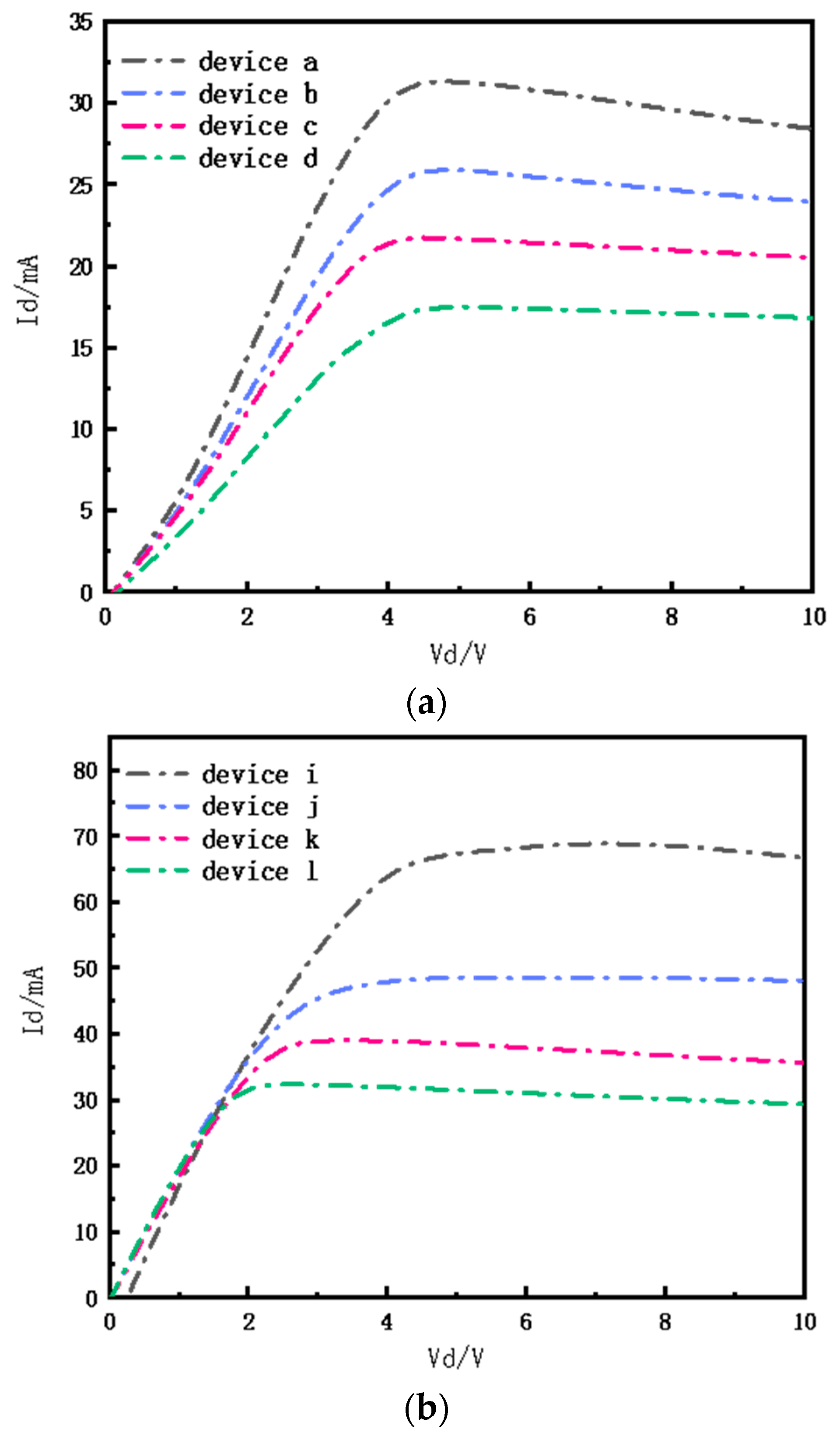
The transfer characteristic curves of conventional and ring-gate HEMT devices are shown in Figure 10a,b when Lgd is 7/11/15/19 μm, respectively. It can be found from the figure that changing Lgd has no obvious effect on the Vth of devices of the two structures; When Vg = 6 V, the output characteristic curves of conventional and ring-gate devices are shown in Figure 11a,b. It can be seen that among conventional devices, device a has the best performance, its Idmax is 31.32 mA when Vd = 4.7 V, which is 79.07% higher than that of device d (17.49 mA); the same trend is also shown in ring-gate devices, the drain saturation current of device i with Lgd = 7 μm reaches 68.80 mA, which is 113.7% higher than that of device l (32.3 mA) with Lgd = 19 μm. This is because the reduction of the source-drain spacing effectively increases the number of additional polarized charges in the gate-drain region, thereby enhancing the polarizaiton coulomb field (PCF) scattering effect on the 2DEG electrons under the gate, making the gate-source channel resistance and the gate-drain channel resistance increase with the decrease of gate bias voltage. Therefore, reducing the source-drain spacing can effectively enhance the PCF scattering effect, thereby improving the output characteristics of the device [18].
In conclusion, an appropriate reduction in the gate-drain spacing of the device is beneficial to improve its output current, lower the on-resistance and make the Vth shift positively, the improvement of these characteristics is beneficial to enhance the safety and reliability of device operation, and make the device better suitable for high-current high-power fields. Meawhile, the output current of the ring-gate device in the above mentioned devices are all obviously higher than those of conventional HEMTs.
4. Conclusions
In this paper, in order to improve the characteristics of traditional AlGaN/GaN HEMT devices, we have carried out an innovative structural design for the gate shape of AlGaN/GaN HEMT devices, a circular-gate AlGaN/GaN HEMT device was proposed and successfully fabricated, and compared with the AlGaN/GaN HEMT device with a conventional strip gate. We found that when Lg = 3 μm, Lgd = 7 μm, the former can achieve higher threshold voltage and output current density, the Vth and Idmax of ring-gate device are respectively 66.7% and 161.8% higher than them of conventional device; then this paper explores the influence of electrode material, structure and size parameters on device performance. After testing, analysis and comparison, it is found that:
When use multi-layer Ti/Al/Ti/Al/Ti/Al/Ni/Au electrodes and the ohmic groove is etched to 10 nm, the device can achieve a larger output current, the Idmax of the ring-gate structure device can reach 79.63 mA, and the conventional device can reach 47.83 mA, compared with devices with single-layer electrodes and no groove etching, this value is increased by 51.07 mA and 36.47 mA, respectively;
When other conditions remain the same and Lg increases, Vth of the device will show a trend of forward drift, while the saturation current of the device decreases instead, and the drop of saturation current of ring-gate HEMT is more obvious, the drain saturation current of the Lg = 6 μm device is 109.4% lower than that of the Lg = 3 μm device;
When Lg is kept constant and Lds is changed, it is found that the drain saturation current decreases with the increase of Lds in the devices of the two structures. The conventional structure device with a Lgd = 7 μm has a 79.07% higher saturation drain current than the one with a Lgd = 19 μm, and the ring-gate device with a Lgd = 7 μm has a 113.7% higher Idmax than the one with Lgd = 19 μm;
In all devices prepared above, we can observe that all ring-gate HEMT devices exhibit higher output current and better turn-on characteristics than conventional structure devices. Under the best preparation conditions and size parameters (using multi-layer Ti/Al electrodes, 10 nm groove etching, Lg = 3 μm, Lgd = 7 μm, Lgs = 5 μm),the output current of the ring-gate HEMT (79.63 mA) is 68.1% higher than that of the conventional HEMT (47.38 mA).
The above results show that the output and transfer characteristics of the device can be greatly improved by changing the gate shape of the AlGaN/GaN HEMT to a ring shape, and the performance of the device can be further optimized by using multiple Ti/Al/Ti/Al/Ti/Al/Ni/Au electrode materials, 10 nm source-drain groove etching and reducing Lg, Lds within a reasonable range. This has positive significance for further improving and optimizing the electrical properties of AlGaN/GaN HEMT devices, and can be beneficial for their applications in high-current, high-power fields.
Author Contributions
Conceptualization, Y.Z., X.S. and F.L.; Methodology, Y.Z. and X.S. and J.L. (Jianwei Li); Experiment, X.S.; Resources, Y.Z.; Data Curation, X.S.; Writing—Original Draft Preparation, X.S.; Writing—Review & Editing, X.S., B.F., P.L. and J.L. (Jinheng Li). All authors have read and agreed to the published version of the manuscript.
Funding
This research was funded by the National Key Research and Development Program of China (Grant No. 2017YFB0402803) and the Natural Science Foundation of Beijing, China (Grant No. 4182011).
Data Availability Statement
The data that support the findings of this study are available from the corresponding author upon reasonable request.
Conflicts of Interest
The authors have no conflict to disclose.
References
- Salah, S.; Olfa, F.; Hassen, M. Effects of gate length on GaN HEMT performance at room temperature. J. Phys. Chem. Solids 2022, 161, 110418. [Google Scholar]
- Koo, S.M.; Kang, M.S. Gate metal dependent electrical characteristics of AlGaN/GaN HEMTs. Mater. Res. Bull. 2014, 58, 178–180. [Google Scholar] [CrossRef]
- Majumdar, S.; Dey, A.; Sahu, R.; Lepcha, G.; Dey, A.; Ray, P.P.; Dey, B. An aromatic acid based supramolecular Zn(II)-metallogel for fabricating light-sensitive metal-semiconductor junction type Schottky diode with satisfactory rectification ratios. Mater. Res. Bull. 2023, 157, 112003. [Google Scholar] [CrossRef]
- Majumdar, S.; Sil, S.; Sahu, R.; Ghosh, M.; Lepcha, G.; Dey, A.; Mandal, S.; Ray, P.P.; Dey, B. Electronic charge transport phenomena directed smart fabrication of Metal-Semiconductor based electronic junction device by a supramolecular Mn(II)-Metallogel. J. Mol. Liq. 2021, 338, 116769. [Google Scholar] [CrossRef]
- Majumdar, S.; Pal, B.; Sahu, R.; Das, K.S.; Ray, P.P.; Dey, B. A croconate-directed supramolecular self-healable Cd(II)-metallogel with dispersed 2D-nanosheets of hexagonal boron nitride: A comparative outcome of the charge-transport phenomena and non-linear rectifying behaviour of semiconducting diodes. J. R. Soc. Chem. 2022, 51, 9007–9016. [Google Scholar] [CrossRef]
- Zhang, N.Q.; Keller, S. High breakdown GaN HEMT with overlapping gate structure. IEEE Electron Device Lett. 2000, 21, 421–423. [Google Scholar] [CrossRef]
- Lee, H.S.; Lee, D.S.; Palacios, T. AlGaN/GaN High-Electron-Mobility Transistors Fabricated Through a Au-Free Technology. IEEE Electron Device Lett. 2011, 32, 623–625. [Google Scholar]
- Zhou, Q.; Liu, L.; Zhang, A.; Chen, B.; Jin, Y.; Shi, Y.; Wang, Z.; Chen, W.; Zhang, B. 7.6 V Threshold Voltage High-Performance Normally-Off Al2O3/GaN MOSFET Achieved by Interface Charge Engineering. IEEE Electron Device Lett. 2016, 37, 1. [Google Scholar] [CrossRef]
- Zhao, S.L.; Wang, Z.Z.; Chen, D.Z.; Wang, M.J.; Dai, Y.; Ma, X.H.; Zhang, C.J.; Hao, Y. 1.8-kV circular AlGaN/GaN/AlGaN double-heterostructure high electron mobility transistor. Chin. Phys. B 2019, 28, 027301. [Google Scholar] [CrossRef]
- Wei, X.; Zhang, X.; Sun, C.; Tang, W.; He, T.; Zhang, X.; Yu, G.; Song, L.; Lin, W.; Cai, Y.; et al. A Novel Normally-off Laterally Coupled p-GaN gate HEMT. In Proceedings of the 2021 5th IEEE Electron Devices Technology & Manufacturing Conference, Chengdu, China, 8–11 April 2021. [Google Scholar]
- Zhu, Y.; Li, J.; Li, Q.; Song, X.; Tan, Z.; Li, J. Effects of multi-layer Ti/Al electrode and ohmic groove etching on ohmic characteristics of AlGaN/GaN HEMT devices. AIP Adv. 2021, 11, 115202. [Google Scholar] [CrossRef]
- Bright, A.N.; Thomas, P.J.; Weyland, M.; Tricker, D.M.; Humphreys, C.J.; Davies, R. Correlation of contact resistance with microstructure for Au/Ni/Al/Ti/AlGaN/GaN ohmic contacts using transmission electron microscopy. J. Appl. Phys. 2001, 89, 3143–3150. [Google Scholar] [CrossRef]
- Mahajan, S.S.; Dhaul, A.; Laishram, R.; Kapoor, S.; Vinayak, S.; Sehgal, B.K. Micro-structural evaluation of Ti/Al/Ni/Au ohmic contacts with different Ti/Al thicknesses in AlGaN/GaN HEMTs. Mater. Sci. Eng. B 2014, 183, 47–53. [Google Scholar] [CrossRef]
- Kong, X.; Wei, K.; Liu, G.; Liu, X. Role of Ti/Al relative thickness in the formation mechanism of Ti/Al/Ni/Au Ohmic contacts to AlGaN/GaN heterostructures. J. Phys. D Appl. Phys. 2012, 45, 265101–265107. [Google Scholar] [CrossRef]
- Van Daele, B.; Van Tendeloo, G.; Ruythooren, W.; Derluyn, J.; Leys, M.R.; Germain, M. The role of Al on Ohmic contact formation on n-type GaN and AlGaN/GaN. Appl. Phys. Lett. 2005, 87, 6214. [Google Scholar] [CrossRef]
- Liu, L.S. An improved gate charge model of HEMTs by direct formulating the branch charges. Chin. J. Electron. 2014, 23, 673–677. [Google Scholar]
- Ruden, P.P.; Albrecht, J.D.; Sutandi, A.; Binari, S.C.; Ikossi-Anastasiou, K.; Ancona, M.G.; Henry, R.L.; Koelske, D.D.; Wickenden, A.E. Extrinsic performance limitations of AlGaN/GaN heterostructure field effect transistors. Mater. Res. Soc. Internet J. Nitride Semicond. Res. 1999, 4, 678–683. [Google Scholar] [CrossRef] [Green Version]
- Cui, P. Research on Carrier Mobility and Related Device Characteristic Parameters of AlGaN/GaN Heterojunction Field Effect Transistors. Doctoral Dissertation, Shandong University, Jinan, China, 27 May 2018. [Google Scholar]
Figure 1.
(a) Cross-sectional view and (b) top view of ring-gate AlGaN/GaN HEMT device.

Figure 2.
(a) 3D image of conventional HEMT device and (b) ring-gate HEMT device.

Figure 3.
Optical microscope image of (a) conventional structure HEMT device (b) ring-gate HEMT device.
Figure 3.
Optical microscope image of (a) conventional structure HEMT device (b) ring-gate HEMT device.

Figure 4.
(a) Comparison of transfer characteristics between conventional and ring-gate HEMT devices. (b) Comparison of output characteristics between conventional and ring-gate HEMT devices.
Figure 4.
(a) Comparison of transfer characteristics between conventional and ring-gate HEMT devices. (b) Comparison of output characteristics between conventional and ring-gate HEMT devices.

Figure 5.
(a) Schematic diagram of the etched area under the source and drain of the conventional structure device and (b) ring-gate structure device.
Figure 5.
(a) Schematic diagram of the etched area under the source and drain of the conventional structure device and (b) ring-gate structure device.

Figure 6.
(a) Output characteristic curve of conventional structure single-layer electrode HEMT device with 10/20 nm etching depth. (b) Output characteristic curve of ring-gate single-layer electrode HEMT device with 10/20 nm etching depth.
Figure 6.
(a) Output characteristic curve of conventional structure single-layer electrode HEMT device with 10/20 nm etching depth. (b) Output characteristic curve of ring-gate single-layer electrode HEMT device with 10/20 nm etching depth.

Figure 7.
(a) Output characteristic curve of conventional structure HEMT device with single and multi-layer electrode when etched depth is 10 nm. (b) Output characteristic curve of ring-gate structure HEMT device with single and multi-layer electrode when etched depth is 10 nm.
Figure 7.
(a) Output characteristic curve of conventional structure HEMT device with single and multi-layer electrode when etched depth is 10 nm. (b) Output characteristic curve of ring-gate structure HEMT device with single and multi-layer electrode when etched depth is 10 nm.

Figure 8.
(a) Transfer characteristic curve of conventional structure HEMT when Lg = 3/4/5/6 μm. (b) Transfer characteristic curve of ring-gate structure HEMT when Lg = 3/4/5/6 μm.
Figure 8.
(a) Transfer characteristic curve of conventional structure HEMT when Lg = 3/4/5/6 μm. (b) Transfer characteristic curve of ring-gate structure HEMT when Lg = 3/4/5/6 μm.

Figure 9.
(a) Output characteristics of conventional structure devices with gate lengths of 3/4/5/6 μm. (b) Output characteristics of ring-gate structure devices with gate lengths of 3/4/5/6 μm.
Figure 9.
(a) Output characteristics of conventional structure devices with gate lengths of 3/4/5/6 μm. (b) Output characteristics of ring-gate structure devices with gate lengths of 3/4/5/6 μm.

Figure 10.
(a) Transfer characteristics of conventional structure devices with Lgd of 7/11/15/19 μm. (b) Transfer characteristics of ring-gate structure devices with Lgd of 7/11/15/19 μm.
Figure 10.
(a) Transfer characteristics of conventional structure devices with Lgd of 7/11/15/19 μm. (b) Transfer characteristics of ring-gate structure devices with Lgd of 7/11/15/19 μm.

Figure 11.
(a) Output characteristics of conventional structure devices with Lgd of 7/11/15/19 μm. (b) Output characteristics of ring-gate structure devices with Lgd of 7/11/15/19 μm.
Figure 11.
(a) Output characteristics of conventional structure devices with Lgd of 7/11/15/19 μm. (b) Output characteristics of ring-gate structure devices with Lgd of 7/11/15/19 μm.


Table 1.
AlGaN/GaN HEMT devices grouping with different electrode structure and etching depth.
| Device | Metal Eletrode Material | Etching Depth (nm) | Grid Shape |
|---|---|---|---|
| 1 | Ti/Al/Ni/Au | 10 | Conventional strip gate |
| 2 | Ti/Al/Ni/Au | 20 | Conventional strip gate |
| 3 | Ti/Al/Ti/Al/Ti/Al/Ni/Au | 10 | Conventional strip gate |
| 4 | Ti/Al/Ti/Al/Ti/Al/Ni/Au | 20 | Conventional strip gate |
| 5 | Ti/Al/Ni/Au | 10 | Ring grid |
| 6 | Ti/Al/Ni/Au | 20 | Ring grid |
| 7 | Ti/Al/Ti/Al/Ti/Al/Ni/Au | 10 | Ring grid |
| 8 | Ti/Al/Ti/Al/Ti/Al/Ni/Au | 20 | Ring grid |
Table 2.
Gruoping of conventional AlGaN/GaN HEMT devices with different gate length and gate-drain spacing.
Table 2.
Gruoping of conventional AlGaN/GaN HEMT devices with different gate length and gate-drain spacing.
| Conventional Devices | Gate Length (Lg/μm) | Gate-Source Spacing (Lgs/μm) | Gate-Drain Spacing (Lgd/μm) |
|---|---|---|---|
| a | 3 | 5 | 7 |
| b | 3 | 5 | 11 |
| c | 3 | 5 | 15 |
| d | 3 | 5 | 19 |
| e | 3 | 5 | 11 |
| f | 4 | 5 | 11 |
| g | 5 | 5 | 11 |
| h | 6 | 5 | 11 |
Table 3.
Gruoping of ring-gate AlGaN/GaN HEMT devices with different gate length and gate-drain spacing.
Table 3.
Gruoping of ring-gate AlGaN/GaN HEMT devices with different gate length and gate-drain spacing.
| Ring-Gatel Devices | Gate Length (Lg/μm) | Gate-Source Spacing (Lgs/μm) | Gate-Drain Spacing (Lgd/μm) |
|---|---|---|---|
| i | 3 | 5 | 7 |
| j | 3 | 5 | 11 |
| k | 3 | 5 | 15 |
| l | 3 | 5 | 19 |
| m | 3 | 5 | 11 |
| n | 4 | 5 | 11 |
| o | 5 | 5 | 11 |
| p | 6 | 5 | 11 |
Publisher’s Note: MDPI stays neutral with regard to jurisdictional claims in published maps and institutional affiliations. |
© 2022 by the authors. Licensee MDPI, Basel, Switzerland. This article is an open access article distributed under the terms and conditions of the Creative Commons Attribution (CC BY) license (https://creativecommons.org/licenses/by/4.0/).
Share and Cite
MDPI and ACS Style
Zhu, Y.; Song, X.; Li, J.; Li, J.; Fei, B.; Li, P.; Li, F. A Novel Ring-Gate AlGaN/GaN HEMT Device and Electrode Structure Optimization. Electronics 2022, 11, 3329. https://0-doi-org.brum.beds.ac.uk/10.3390/electronics11203329
AMA Style
Zhu Y, Song X, Li J, Li J, Fei B, Li P, Li F. A Novel Ring-Gate AlGaN/GaN HEMT Device and Electrode Structure Optimization. Electronics. 2022; 11(20):3329. https://0-doi-org.brum.beds.ac.uk/10.3390/electronics11203329
Chicago/Turabian StyleZhu, Yanxu, Xiaomeng Song, Jianwei Li, Jinheng Li, Baoliang Fei, Peiyang Li, and Fajun Li. 2022. "A Novel Ring-Gate AlGaN/GaN HEMT Device and Electrode Structure Optimization" Electronics 11, no. 20: 3329. https://0-doi-org.brum.beds.ac.uk/10.3390/electronics11203329
Note that from the first issue of 2016, this journal uses article numbers instead of page numbers. See further details here.