
Prototyping Power Electronics Systems with Zynq-Based Boards Using Matlab/Simulink—A Complete Methodology


1
Instituto de Telecomunicações, University of Coimbra, Pole 2, 3030-290 Coimbra, Portugal
2
Department of Electrical and Computer Engineering, University of Coimbra, Pole 2, 3030-290 Coimbra, Portugal
*
Author to whom correspondence should be addressed.
Electronics 2022, 11(7), 1130; https://0-doi-org.brum.beds.ac.uk/10.3390/electronics11071130
Submission received: 8 February 2022
/
Revised: 25 March 2022
/
Accepted: 31 March 2022
/
Published: 2 April 2022
(This article belongs to the Special Issue Power Converter Design, Control and Applications)
Abstract
:Many advanced power electronics control techniques present a steep computational load, demanding advanced controllers, such as FPGAs. However, FPGA development is a daunting and time-consuming task, inaccessible to most users. This paper proposes a complete methodology for prototyping power electronics with Xilinx Zynq-based boards using Matlab/Simulink and HDL Coder. Even though these tools are relatively well documented, and several works in the literature have used them, a methodology for developing power electronics systems with them has never been proposed. This paper aims to address that, by proposing a complete programming and design methodology for Zynq-based power electronics and discussing important drawbacks and hurdles in Simulink/HDL Coder development, as well as their possible solutions. In addition, techniques for the implementation of all required peripherals (ADCs, digital outputs, etc.), system protections, and real-time data acquisition on Zynq boards are presented. This methodology considerably reduces the development time and effort of power electronics solutions using Zynq-based boards. In addition, a demonstration Simulink model is provided with all proposed techniques and protections, for use with a readily available development board (Zedboard) and ADC modules. This should further reduce the learning curve and development effort of this type of solution, contributing to a broader access to high-performance control prototyping using Zynq-based platforms. An application example is presented to demonstrate the potential of the proposed workflow, using a Zedboard to control a multilevel UPS inverter prototype with Model Predictive Control.
1. Introduction
Over the last years, many advanced computation and control techniques have been proposed for power electronics. These advanced techniques include solutions such as Model Predictive Control [1,2] or Artificial Intelligence [3], which have proven to be highly advantageous in the fields of energy conversion and power electronics, resulting in significant interest from both the scientific and industrial community. For example, Model Predictive Control (MPC) has shown to be highly advantageous in power electronics, providing good steady-state performance and excellent dynamic response [1,2]. In addition, this type of controller allows the simultaneous pursuit of multiple independent (and often conflicting) objectives and easy inclusion of system non-linearities and constraints. Hence, it is highly advantageous for the control of complex multi-objective and multi-converter systems, in all kinds of applications [1,2], such as wind generation [4], UPS systems [5,6] or microgrids [7,8].
However, these advanced control techniques typically present a critical limitation: they carry a very high computational burden. This characteristic makes their practical implementation extremely difficult. It was only in recent years that available control platforms have become sufficiently powerful to enable broader study and use of these types of computational solutions. The overall complexity of power electronics converters has also significantly increased in the last decades due to the adoption of more complex topologies (such as multilevel converters with an increasing number of levels) and more complex systems and applications (such as multi-phase machines [4], modular/paralleled converters [5], or multi-converter systems [5,6]). Using techniques such as MPC leads to an enormous increase in the computational load of the controller. In addition, techniques like MPC require high sampling frequencies, which means all computations must be completed consistently within a very short period (tens of microseconds). Furthermore, the controller must ensure precise timing and perfect synchronization between the acquisition of multiple signals and numerous control inputs and outputs. These requirements greatly hinder the practical implementation of advanced control techniques in power electronics and lead to a critical need for new (affordable and industrially viable) control platforms with very high processing power.
In the context of power electronics development, control platforms can typically be divided into two types: rapid-prototyping solutions and custom platforms. Rapid-prototyping solutions are mainly directed to development and laboratory use, presenting easy-to-use interfaces, numerous safety features, and dedicated development tools that enable fast and easy programming. However, these solutions typically present very high costs, making them unviable for industrial use and inaccessible to many small companies and research groups. On the other hand, custom-developed platforms provide significantly lower costs and perfectly fit the specific needs of a specific product or application. However, this type of solution typically requires dedicated hardware development and complex and time-consuming programming using low-level tools. For this reason, this type of approach is generally not appropriate for research purposes or initial development stages.
Currently, most rapid-prototyping solutions found on the market are based on central processing units (CPUs) or digital signal processors (DSPs), which provide simple and versatile programming, ideal for fast testing and development, with a low programming effort. This approach can be found in products from dSPACE, OPAL-RT, Speedgoat, National Instruments, and others. However, the sequential execution nature of processors limits their processing throughput, limiting the sampling frequencies achievable with complex control systems. Moreover, the sequential nature of processors and the need to switch between multiple tasks limit their ability to ensure perfect timing in input and output (I/O) management and hinder synchronization between different interfaces (such as the ADC sampling and output signal updates). For this reason, several rapid-prototyping platforms now use an FPGA to manage the I/O, in addition to the processor. This allows precise interface control and enables critical parts of the code to be implemented in the FPGA, taking advantage of its parallel execution. The code generation and deployment of rapid-prototyping solutions differ from brand to brand but typically rely on well-known software tools for programming. For example, dSpace, OPAL-RT, and Speedgoat rely on Matlab/Simulink for model-based development, while National Instruments solutions use Labview. On the other hand, many platforms use dedicated proprietary tools for monitoring and interface development (for example, Control Desk from dSpace and RT-LAB from OPAL-RT).
Despite their many advantages, including their ready-made nature and easy programming, rapid-prototyping platforms typically share a common problem: a very high cost. For this reason, researchers frequently resort to lower-cost solutions, such as development boards. While cheap DSPs have historically been a go-to solution for low-cost prototyping of power electronics, they lack the processing power required to control complex systems with advanced control algorithms, such as MPC. Given the steep processing and timing requirements of this type of controller, FPGAs become one of the main options for prototyping. FPGAs offer a high processing capacity and throughput due to their parallel computing capabilities, enable precise I/O timing and synchronization, and guarantee a deterministic processing time. These advantages make FPGAs ideal for advanced controller implementation. However, FPGA programming can be a daunting and time-consuming task, requiring highly specialized hardware description language (HDL) knowledge. The HDL Coder tool found in Matlab/Simulink significantly simplifies FPGA programming, by providing automatic HDL code generation from a model-based Simulink design. This significantly speeds up FPGA development and eliminates the need for HDL expertise [9,10,11,12].
Regardless of the used programming technique, debugging and data acquisition can be highly problematic on FPGAs since it is very difficult to have external access to internal variables in real-time, and user interface implementation is also a significant challenge. Hybrid System-on-Chip (SoC) solutions, which include both an FPGA and a processor, partly solve this problem by simultaneously providing the determinism and high processing power of FPGAs and the simple connectivity and user interface of a processor. Furthermore, a dedicated communication interface between the FPGA and processor enables easier data capture and variable visualization, making this solution advantageous for prototyping. Xilinx Zynq chips are the most common hybrid SoCs and are available on numerous development boards.
Despite the clear advantages of Zynq SoCs, their programming is still very complex, especially for non-experts. However, it is now possible to use Matlab/Simulink to program these chips entirely using model-based techniques. HDL Coder enables a direct generation of HDL code for the FPGA directly from Simulink models, while Embedded Coder enables code generation for the ARM processor found on Zynq chips. This reduces (or even eliminates) the need for low-level programming and makes prototyping with these chips viable to non-experts. Additionally, it is possible to simulate both the processor and FPGA response directly from Simulink, shortening the development time. Given the low cost of many Zynq-based development boards, these SoCs become an excellent choice for low-cost prototyping with advanced control techniques.
Various work can be found in the literature taking advantage of both standalone FPGAs [11,12,13,14,15] and Zynq SoCs [10,16,17,18,19,20,21,22,23,24,25] to control power electronics devices. Most presented Zynq-based solutions use development boards for prototyping [10,17,19,20,21,22,24,25], including the Zedboard used in this paper [10,19,20,21,24]. A custom hardware platform is proposed in [17] specifically for power electronics control. In [18], a high-performance custom control platform is also proposed for power electronics, using the higher-end Ultrascale+ family of Zynq chips, for ultra-high performance (but with significantly higher cost).
Many FPGA-based solutions found on the literature rely on conventional low-level coding (typically using HDL and C on Xilinx tools) [16,17,20,21,23]. Other solutions use the Xilinx System Generator toolbox in Matlab/Simulink, to enable model-based design [19,24]. However, despite providing a model-based design approach, this tool does not provide some of the advantages of HDL Coder, such as several automatic optimization and pipelining options, automatic delay balancing, assisted fixed-point design, or the use of regular Simulink blocks (much more intuitive for Simulink users).
Several solutions found on the literature have used Matlab/Simulink and HDL Coder [10,11,12,13,14,15,25] for FPGA programming, including on Zynq chips [10,25]. However, even though these works use these tools for experimental implementation, they do not discuss their use, the programming philosophy, or their limitations. Therefore, even though these papers discuss the advantages of using HDL Coder, they do not provide any information on its use or the development process. In fact, several papers mention only a partial use of HDL Coder, to generate the HDL code for a given algorithm, then using other development tools (such as the Xilinx Vivado suite) for final programming and deployment. This paper proposes a complete methodology to fully program the FPGA of Zynq-based boards using Simulink and HDL Coder and to deploy the code into the platform.
Furthermore, the programming of the ARM processor in Zynq-based boards using the Embedded Coder tool is not typically leveraged by the solutions found in the literature—low-level development tools are typically adopted or the processor is not extensively used. In [18], the authors discuss the advantages of using Embedded Coder for partial development of the ARM processor code. However, it is only used to generate a C code for specific algorithms, with that code being manually integrated into a more complex code using low-level tools. Hence, Embedded Coder is not used for the overall programming of the ARM processor nor for direct deployment. The use of this tool is also only briefly mentioned, but not discussed. To the best of the authors’ knowledge, no solutions found in the literature have yet used the HDL Coder and Embedded Coder tools to fully program and deploy power electronics control and monitoring solutions in Zynq-based boards, in power electronics applications. This paper proposes a complete methodology and workflow to design and deploy power electronics solutions entirely from the Matlab/Simulink environment, without the need for interaction with additional tools or low-level coding (neither C nor HDL).
In addition to the design methodology and development workflow, this paper extensively covers the real-time monitoring of power electronics systems from Simulink, using Zynq-based boards. This presents a crucial advantage for debugging and fine-tuning control algorithms implemented in the FPGA for real-time execution, not possible when using stand-alone FPGAs (even if programmed using HDL Coder). In [18], a custom interface is proposed for real-time monitoring, but it relies on custom code and therefore implies development outside Matlab/Simulink, with low-level coding tools.
Even though the tools provided by Mathworks are relatively well documented and make prototyping with Zynq devices significantly easier, their setup and use are not entirely straightforward and can present a steep learning curve. For this reason, this paper presents a detailed description on setting up and using all the necessary tools. The proposed design methodology is then described in detail. This paper does not merely show how to use the software tools, but instead presents a complete programming philosophy and design methodology, from peripheral management to real-time monitoring. This includes the analysis of several drawbacks of HDL Coder’s automatic code generation for real-time power electronics control and solutions to overcome them.
This paper also proposes techniques for the implementation of all peripheral hardware typically required for power electronics (ADCs, isolated digital outputs, etc.) and to overcome possible controller limitations, such as insufficient input/output ports. Several protection mechanisms are also proposed for safe power electronics prototyping. The proposed solution allows a continuous real-time monitoring of any number of waveforms and internal controller variables using Simulink External mode. A technique is also proposed to perform lossless data acquisition (with no undersampling) of limited time windows.
A demonstration model is provided by the authors, with the proposed techniques and peripheral management code pre-implemented, for immediate testing on a commercially available development board—a Zedboard—and with off-the-shelf ADC modules. This provides the reader with a low-cost, easy-to-use starting point to test the proposed techniques and start prototyping power electronics systems using the proposed methodology. This should significantly reduce the learning curve and development effort of this type of solution, contributing to a broader access to high-performance power electronics control using Zynq-based platforms.
To demonstrate the potential of this type of controller for advanced control of power electronics converters, the Zedboard is used to control a multilevel inverter using Model Predictive Control. Experimental results are presented for the proposed techniques and for the UPS application example.
To summarize, the main contributions of this paper are as follows:
- A complete design methodology for power electronics using Zynq-based boards and Matlab/Simulink tools is proposed for the first time.
- The proposed methodology allows programming of both the FPGA and ARM processor found in Zynq-based boards entirely from the Simulink graphical environment, with no low-level coding. Previous solutions found in the literature typically program only the FPGA using Simulink and often for partial development (completed in low-level tools). Few previous solutions have used Simulink to program the ARM processor in Zynq chips for power electronics applications, and none have used it for complete development (FPGA+ARM) and real-time deployment and monitoring, entirely from Simulink (with no additional tools or coding).
- The proposed methodology allows continuous real-time monitoring of power electronics systems with Zynq-based boards directly from Simulink, with no need to develop custom interface tools. This presents a vital advantage for FPGA control algorithm implementation, since it enables easy real-time access to any internal control variable—critical for debug and controller tuning. A technique for data acquisition with no sample loss is also proposed.
- Analysis of several HDL Coder drawbacks for power electronics control, such as unreliable processor execution cycles or peripheral timing corruption due to automatic delay balancing, is not properly described in the literature. Techniques are proposed in this research to avoid/mitigate these problems.
- This paper also includes a proposal of hardware peripheral management techniques and protection mechanisms to stop power converter operation in case of over-current, over-voltage, processor lock (crash), or loss of communication with the host computer.
- We also provide distribution of a Simulink demonstration model including all proposed programming techniques and hardware management solutions, for easy and immediate reproduction and testing by the reader, using commercially available development board and ADC modules.
This type of detailed study and proposal of a development methodology for rapid prototyping of power electronics using Zynq-based devices has never been available in the literature. Furthermore, the distribution of ready-to-use solutions (Simulink code made available for direct use) provides a major contribution for research groups, educators, and companies to be able to use these tools for power electronics prototyping, significantly reducing the development time and effort.
This paper is organized as follows: in Section 2, the hardware requirements for power electronics control are analyzed and possible implementations are discussed. In Section 3, the proposed design philosophy for Zynq SoCs from Matlab/Simulink is presented. Section 4 presents the required software tools and respective setup process. Section 5 is the main section of the paper and presents the proposed development methodology for Zynq-based boards using Simulink. Section 6 presents a power electronics application example controlled using a Zedboard. Lastly, Section 7 presents the final conclusions.
2. Control platform Hardware Requirements for Power Electronics Control
Power electronics systems can present radically different structures, with different converter topologies and applications. Thus, hardware requirements change significantly depending on the system and its defined requirements. For example, the number and type of sensors and the number of semiconductors to control varies significantly depending on the target application and converter topology. The connectivity requirements of the system can also significantly vary, ranging from no connectivity at all (fully standalone operation) to networked or internet-connected applications (critical for the industry 4.0 paradigm).
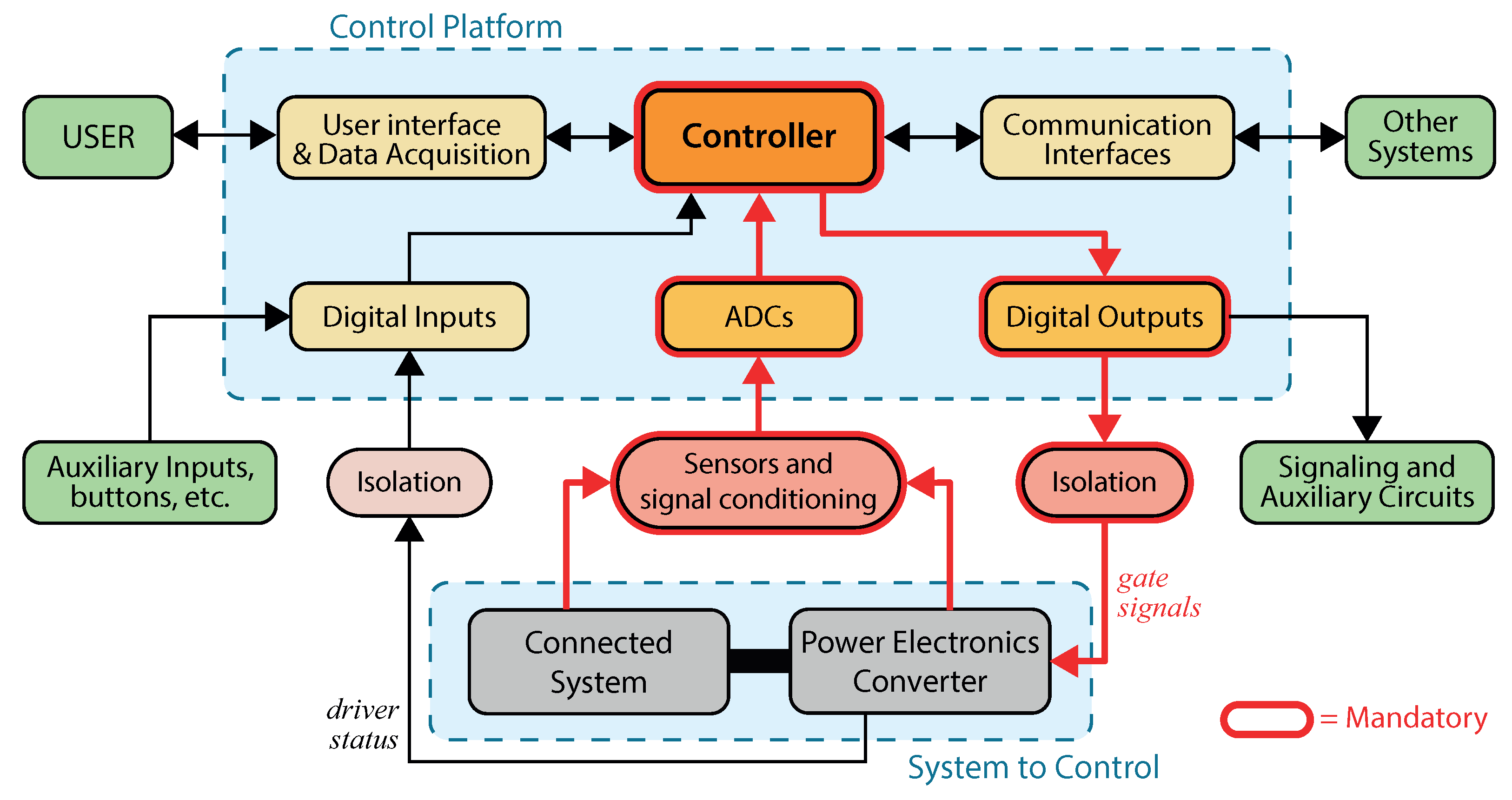
Figure 1 presents a simplified representation of some of the most common controller interfaces and peripheral hardware required for power electronics converter control.
As shown in the figure, many distinct controller interfaces can be used in power electronics control for different purposes. However, some interfaces are mandatory and can be found in all power electronics controllers (highlighted in red in Figure 1):
- Digital outputs for power switch gate signals;
- Analog inputs for sensor data acquisition.
Without these interfaces, closed-loop power converter control would be impossible. Other interfaces can also be highly advantageous for power electronics design and control but are not found in all applications. Some of the most common examples are:
- User interface and data acquisition—enables data visualization, debugging, and parameter tuning;
- Gate driver status readout—useful when gate drivers provide status/error signals;
- Communication interfaces for interaction with other systems (e.g., other controllers), internet connectivity or remote monitoring;
- Digital inputs/outputs for auxiliary signals, such as panel signaling and command.
All listed interfaces can be implemented in several manners. This paper presents simple and inexpensive ways to implement these interfaces for prototyping using Zynq-based controllers. The requirements for each interface and proposed implementations are presented below.
2.1. Main Controller
The most critical component of the control platform is the main controller board. In the context of this paper, the main controller is assumed to be a Zynq-based board. Using a Zynq-based controller enables both the precise peripheral control and deterministic execution of an FPGA and the simple connectivity of a processor. In this paper, a commercially available Zedboard development kit is used. This board was selected due to its wide availability, comprehensive documentation, and vast community support. Additionally, this board is pre-supported by HDL Coder and Embedded Coder, which means no manual board configuration is required to start programming the board from Matlab/Simulink. This is ideal for the first contact with Zynq-based development from Simulink, making setup easier for new users.
2.2. Analog to Digital Converters (ADCs)
Analog inputs are essential in power electronics systems, as they define how the controller perceives the state of the system. ADCs must have an acceptable level of precision and a sufficiently high sampling frequency. In addition, all ADC channels must be sampled simultaneously—this is especially important in many advanced control techniques, such as MPC.
For easy implementation and reproduction, commercially available ADC modules are used in this paper, specifically Pmod AD1 modules from Digilent [26]. Each module provides two simultaneously sampled ADC channels with a 12-bit resolution and up to 1 million samples per second. Each module can be directly plugged into a Pmod connector on the Zedboard, making prototyping and experimenting very practical. The controller must read data from the ADC modules using serial communication (implementation discussed in Section 5).
2.3. Digital Inputs and Outputs
Digital inputs and outputs (I/O) are the most common interfaces found in control boards, reading or writing binary signals. In power electronics, digital outputs are critical for activating the power switch gate drivers. Digital inputs and outputs can also be used for other purposes, such as interacting with auxiliary circuits, reading back gate driver status or activating signaling (such as panel lighting). Hence, in complex power electronics systems, such as those with multiple converters or multilevel topologies, a tremendous amount of digital ports may be required.
Since most Zynq-based development boards have limited FPGA ports available externally, these may be insufficient to implement all necessary peripherals directly. In this case, several techniques can be used to overcome the limitation.
Most converter topologies use complementary signals to activate pairs of power switches: Thus, it is possible to generate control signals for only half the switches and use external logic to invert those signals for the remaining switches. However, this makes it impossible to simultaneously deactivate all switches (which might be necessary for safety reasons). It also makes it impossible to generate a deadtime between the activation of complementary switches. For this reason, this technique is not considered in this paper. Instead, different approaches are proposed to increase the number of available digital outputs (or inputs). These approaches are schematically represented in Figure 2 for the output case (inputs can be implemented analogously).
If the used board has sufficient ports for all peripherals, each digital port can be controlled directly by an FPGA port, as shown in Figure 2a. This is the easiest option to implement and the most reliable. The gate activation signals must be isolated from the potential of the power switch, not only to prevent short-circuits between different points of the converter but also to protect the controller from any phenomena on the power circuit. Optocouplers or digital isolators typically ensure this isolation. In this paper, SI8237 digital isolators [27] are used, simultaneously providing isolation and level shifting from the 3.3 V found on the Zedboard ports to 15 V, the voltage level required by the used gate drivers. An analogous approach can be used for digital inputs.
If sufficient ports are not available, it is possible to use serial-to-parallel shift registers to convert a single data line (streamed serially) into a high number of outputs. This solution, represented in Figure 2b, allows almost infinite expansion of the available outputs, with very few data lines. However, the output port update time increases with the number of signals, so a very long chain is not recommended. The non-negligible port update time means this solution may not allow a reliable generation of deadtimes or the implementation of modulators. This solution is therefore better suited for low-speed non-critical outputs. In this paper, BU4094BCF shift registers [28] are used, associated in a daisy chain. This way, only four data lines are needed on the Zynq FPGA-serial clock, data line, strobe, and output enable. Furthermore, only four digital isolators are required, instead of one for each channel. The used SI8237 isolators translate the signals to 15V, and the shift registers operate directly at this voltage—this significantly reduces system cost compared to individual isolators for all outputs. An analogous approach can be used for reading inputs, using parallel-to-serial shift registers.
A more advanced solution, illustrated in Figure 2c, is to use a secondary (low-cost) FPGA uniquely for port management. The main advantage of this approach is its extremely high versatility. Since each output is controlled directly by an FPGA, deadtimes can be precisely controlled, and modulation techniques can be easily implemented. The Zynq controller sends commands to the secondary FPGA over a communication bus, so only a few ports are needed on the Zynq board. The secondary FPGA is intended only for I/O management and does not perform intensive calculations. Thus, very cheap FPGA boards with a high number of ports can be used. This paper uses a Spartan 7 FPGA board (S7 Mini from Trenz [29]), which has 64 available FPGA ports. Even cheaper FPGA boards can be found (e.g., Spartan 6 or Spartan 3 FPGAs). However, the Vivado tools only support Xilinx 7-series FPGAs. Thus, a 7-series FPGA was selected to enable its programming from Simulink (discussed in Section 5.8.4).
The communication interface with the secondary FPGA can be implemented in many different ways, but a simple serial communication approach is proposed in this paper. This approach requires only three output ports: two for communication (a serial clock and a data line) and one output clock that indicates the start of the sampling period. The synchronization with the secondary FPGA is implemented as shown in Figure 3.
As shown in Figure 3, the controller has a given (deterministic) calculation time. When all calculations are complete, the main controller (Zynq) immediately sends the switching states (or duty cycles) to be applied in the next sampling period to the second FPGA. This way, the secondary FPGA receives this information before the next sampling instant. When the next sampling period begins (indicated by the cycle_start bit), the secondary FPGA applies the new states (or updates the duty cycle of the modulator, if one is used). This guarantees near-perfect synchronization between the analog sampling and digital output activation, making this solution perfect for critical signals and signals with strict timing requirements, such as the power switch gate signals.
In addition to outputs, the secondary FPGA can also be used to manage inputs. If bidirectional communication is implemented, it can read inputs and return their value to the Zynq-based controller.
2.4. User Interface and Data Acquisition
In this paper, all user interface and acquisition functions are performed using Matlab/Simulink and supporting Add-Ons. This toolchain allows easy simulation and programming of both the FPGA and processor components of the Zynq platform. The Zynq board is network-connected to a host computer (via ethernet in the Zedboard case). The host computer can monitor and control the system in real-time, allowing the user to acquire data from the platform and alter controller parameters. The controller programming philosophy and workflow are discussed in the following sections.
3. Proposed Design Philosophy for Zynq SoCs using Matlab/Simulink
Mathworks currently provides two workflows/add-ons for programming Zynq devices: the Embedded Coder Hardware Support Package for Xilinx Zynq Platform and the SoC Blockset Support Package for Xilinx Devices. These two solutions offer different features and model design philosophies, but both enable the programming of the FPGA and ARM processor in Zynq chips, and communication between them. The main difference found when using these two solutions is a different Simulink model structure. While the Embedded Coder Hardware Support Package implements all code (for both FPGA and processor) in the same Simulink model, the SoC Blockset uses different Simulink models (files) to implement each component (FPGA/processor), with a third model being used to interconnect the two and explicitly define the communication interfaces. The SoC Blockset add-on offers additional communication features between the FPGA and processor, such as Direct Memory Access and interrupts. However, these advanced communication mechanisms have proven unreliable with low executions times (tens or even hundreds of microseconds), such as those required in power electronics applications (confirmed by Mathworks support). For this reason, these features are not particularly helpful in the context of power electronics prototyping, addressed in this paper.
Even though the model implementation differs significantly between the Embedded Coder Hardware Support Package and SoC Blockset, both add-ons can be used for power electronics control and prototyping with Zynq boards, using the proposed development philosophy, coding solutions, and peripheral implementations. The choice between these two add-ons ultimately comes down to a personal preference or a given feature that might be advantageous for a specific application. In this paper, the Embedded Coder Hardware Support Package will be used, since the authors have found it more intuitive and easier to use for the proposed development. For this reason, the presented workflow setup instructions and Simulink models are targeted at this specific tool. Nonetheless, the proposed power electronics development methodology with Zynq boards can be directly transposed for use with the SoC Blockset, if preferred. The Simulink model organization and communication blocks will differ, but the development methodology will be the same, including the controller design philosophy, timing definition, delay management techniques, data acquisition, peripheral management, protection mechanisms, etc.
Due to the existence of two processing units in hybrid SoCs (FPGA and ARM processor), algorithms can generally be implemented in three different ways:
- Algorithms can be executed uniquely on the ARM processor;
- Algorithms can be executed uniquely on the FPGA;
- Algorithms can be jointly executed on processor and FPGA—co-processing.
Execution entirely on the ARM is the easiest to achieve since programming a processor is significantly easier than programming an FPGA. This is also true when using Matlab/Simulink since most Simulink blocks are supported by Embedded Coder and can be directly used for code generation (the same model used in simulation). Hence, this is the fastest and easiest way to implement an algorithm on a Zynq SoC. However, the processor presents limited processing power and cannot achieve low sampling times reliably. Furthermore, precise timing is not guaranteed, and I/O management at high frequencies is nearly impossible. Thus, this design philosophy is typically not viable for power electronics control with Zynq-based controllers.
On the other hand, the parallel nature of the FPGA allows a massive amount of calculations to be performed in very little time, enabling very high sampling frequencies to be achieved. More importantly, the execution is entirely deterministic, which means there is no execution time variability. The highly accurate timing of FPGAs also allows precise timing and synchronization of I/Os. Thus, running an algorithm entirely on the FPGA is typically the solution with the best possible performance. However, FPGA programming is significantly more complex and requires a different programming philosophy to leverage the parallel execution capabilities. Additionally, the limited access to internal FPGA variables makes debugging and data acquisition very hard and hinders interaction between the user and the algorithm.
When co-processing an algorithm, its execution is divided between the FPGA and processor, leveraging the advantages of both. This way, critical or calculation-intensive parts of the algorithm can be executed on the FPGA, taking advantage of its parallelism. At the same time, the processor can be used for connectivity, user interface, or to run parts of the algorithm. Running part of the code on the processor can have several advantages. For example, if a high amount of floating-point or double-precision calculations need to be performed, it may be preferable to execute them on the processor since the FPGA has limited resources to perform these operations (DSP slices). Thus, using both processing units to execute a given algorithm provides higher design flexibility and can be highly beneficial.
The main disadvantage of co-processing a given algorithm is that both the FPGA and processor need to respect strict timing requirements to ensure correct execution. For example, in power electronics control, all controller calculations must be completed within a sampling period. If the control algorithm is co-processed, each processing unit must finish its calculations in a given (very short) time and return the resulting data to the other. While the FPGA has a deterministic calculation time, the CPU does not-the execution time varies. Thus, if the processor fails to perform all calculations on time, the FPGA will use the wrong data to perform the following steps, leading to incorrect results and non-optimal control action. This is particularly problematic when high sampling frequencies are used.
With the used development board (Zedboard) and the Operating System (OS) image provided by Mathworks, it was found that the ARM processor could not operate with low sampling times reliably, leading the controller to skip execution in some sampling instants (as confirmed by Mathworks support). This is shown in Section 5.6.
For this reason, the controller execution itself cannot be co-processed in this platform, at least for advanced control algorithms, such as MPC (with a high computational load and low sampling times). Hence, the control algorithm must be fully implemented in the FPGA. However, this does not mean that the ARM processor is not used. Even though the control algorithm is fully implemented in the FPGA, the overall proposed prototyping system uses a co-processing approach. The processor is used for all supporting features, such as controller variables visualization, data acquisition, and parameter changes. These features are critical for debugging and safe converter control, but can be executed at a lower frequency.
The HDL Coder tool found in Matlab/Simulink features two Processor/FPGA synchronization methods: free-running and co-processing. In co-processing mode, the tool automatically generates synchronization logic to synchronize the FPGA code with the processor. This guarantees that the FPGA waits for data from the processor and vice versa. However, in this implementation, the FPGA acts as a slave—it is the processor that controls the timing of execution and sampling time. Thus, the FPGA can no longer guarantee precise peripheral timing, and the sampling time may vary. While this may be appropriate for other applications, it is unacceptable in power electronics control, especially given the lack of CPU execution reliability with low sampling times. Thus, the co-processing mode of HDL Coder should be avoided when prototyping power electronics systems.
In free-running mode, no synchronization mechanism is implemented between the FPGA and processor. However, since the control algorithm and all peripheral management are executed uniquely on the FPGA, this does not carry any negative consequence. This mode must be used for power electronics control using HDL Coder. The overall adopted implementation philosophy is shown in Figure 4.
As shown in the figure, the FPGA is responsible for all interface management (using the available FPGA ports) and the execution of the real-time control algorithm. The ARM processor communicates with the FPGA through an AXI interface, receiving data from the FPGA and sending new parameter values to the controller. The ARM code executes at a lower frequency, to ensure execution reliability. The processor communicates with a host computer executing Simulink in External Mode. From this computer, the user can visualize and save data from the controller and manually alter control parameters.
The platform is programmed using the workflow illustrated in Figure 5. The user initially designs the algorithms in a single Simulink model, with all code to be executed on the FPGA under a single subsystem. Then, the HDL Coder tool generates HDL Code for the specified platform and uses the Xilinx Vivado tools to synthesize that code for the FPGA (in the background). HDL Coder also automatically generates an interface model for programming the processor. In this model, the FPGA subsystem is replaced by the appropriate AXI interfaces to read/write data from/to the FPGA. This model is then used to generate code for the processor (using the Embedded Coder tool) allowing the real-time monitoring and control of the system.
4. Development Workflow Setup
The presented development workflow requires several tools and components to be properly configured. The overall setup process is schematically represented in Figure 6 and described in detail below.
The following software tools are required to develop and deploy control algorithms from Matlab/Simulink to Zynq-based platforms:
- Matlab/Simulink with HDL Coder Toolbox and Embedded Coder Toolbox.
- Xilinx Vivado (System Edition is recommended, but the free Webpack can be used if the chosen board is supported).
It is important to note that compatible versions of the two software tools must be installed. Each HDL Coder release supports only one version of the Vivado Design Suite, which can be found in [30]. For the results presented in this paper, Matlab R2019b and Vivado 2018.3 were used. It should be noted that if Vivado System Edition is used, the “System Generator” tool does not officially support the Matlab version required for HDL Coder compatibility, so it is necessary to manually alter the list of compatible versions for the tool to interact with Matlab (steps found on [31]). If Vivado System Edition is used, it is recommended to start Matlab using the System Generator tool, which automatically configures the connection to Xilinx tools. Otherwise, the HDL generation tool must be configured manually every time Matlab is opened (using the command hdlsetuptoolpath(‘ToolName’,‘XilinxVivado’,‘ToolPath’,‘C: \Xilinx\Vivado\2018.3\bin\vivado.bat’), with the appropriate Vivado version).
The following Matlab Add-Ons must be installed from the Add-On Explorer:
- HDL Coder Support Package for Xilinx Zynq-7000 Platform.
- Embedded Coder Support Package for Xilinx Zynq-7000 Platform.
- A supported compiler (MinGW-w64 is a practical choice, which can be installed directly from the Matlab Add-On Explorer).
Next, it is necessary to configure the add-ons for the correct hardware board. In order to use the HDL Coder, a board definition is required, which defines the target FPGA and respective interfaces. The add-on natively supports several development boards, which include the Zedboard used in this paper. For any of these boards, the tool includes pre-configured board definition files, so no manual setup is required.
If the target platform is not pre-supported by HDL Coder, it is necessary to create a custom board definition to enable FPGA code generation from Simulink. With appropriate board definition files, the HDL Coder tool can generate code for any Xilinx board supported by the used Vivado version. The board files can be found in C:\ProgramData\MATLAB\SupportPackages\R2019b\toolbox\hdlcoder\supportpackages\zynq7000, where R2019b should be replaced with the correct Matlab version. Custom boards should be added here, according to the instructions found on [32]. After adding a custom board, Simulink is able to generate code for its FPGA.
To program the ARM processor from Simulink, the Embedded Coder Support Package for Xilinx Zynq-7000 Platform must also be configured. This requires the board to run an OS which supports all features and libraries required by the tool, enabling communication and programming directly from Simulink. Several development boards are natively supported by this Add-On (including the Zedboard). For these boards, pre-configured OS images are included. In this case, the user only needs to run the add-on setup from the Matlab Add-On Manager. This provides a setup wizard which writes the OS image to the target SD card and configures the network interface for communication with the board. Pre-configured files for other boards can also be found on the official Mathworks GitHub [33] or in community forums.
If the desired board is not pre-supported by Mathworks or the community, it is also possible to generate a custom Linux OS image using the Buildroot tools provided by Mathworks [33] or building a custom Petalinux image with all required libraries. However, this process depends on the target platform and requires a high level of familiarity with Linux OS building and these specific tools, so it will not be discussed in this paper. Additionally, if the user does not want to program the ARM processor using Simulink (only the FPGA), the Embedded Coder Support Package setup can be skipped.
This paper focuses uniquely on prototyping with Zynq-based boards entirely from Simulink, taking advantage of both the FPGA and processor, so both the HDL Coder and Embedded Coder tools are used. Given that the used board (Zedboard) is entirely supported by both tools, the initial setup is fast and effortless. This makes the Zedboard a perfect platform for initial testing of the proposed development workflow and for lab-oriented prototyping.
5. Proposed Zynq-Based Development Methodology Using Simulink
The proposed development methodology makes it possible to program and control a Zynq-based controller (a Zedboard in this case) directly from Matlab/Simulink. This way, low-level C and HDL coding is not necessary, and programming can be done using a significantly simpler graphical model-based approach. System monitoring and control can also be done directly from the Simulink graphical interface. This section discusses the main steps and techniques for prototyping power electronics systems using this workflow. As an addition to this paper, an example Simulink model can be found in [34], to help new users get started with this development methodology. This demo provides the Simulink code implementation of the all proposed design techniques, allowing readers to easily and quickly implement the proposed prototyping solutions.
5.1. Simulink Model Structure
When developing code for Zynq-based chips, the Simulink model must clearly separate the contents to be executed in the FPGA and processor. This is done by creating a single subsystem that includes all content to be executed on the FPGA. This is shown in Figure 7, for the case of the demo provided in [34].
In the model shown in Figure 7, the subsystem named FPGA contains all code to be executed on the FPGA of the Zedboard. The code inside this subsystem will be used directly for HDL code generation. The overall Simulink model can be used to accurately simulate the response of the entire system (FPGA+processor). Everything outside the FPGA block will be used to create a new model for programming the ARM processor (denoted as interface model in Simulink).
When designing the overall Simulink model, the user must carefully define the sampling time and data types to be used in the FPGA. Each port on the FPGA subsystem translates directly to an AXI interface register (or registers) for communication with the processor or to a physical FPGA I/O port (or multiple ports). When using different sampling times in the FPGA and processor (as proposed in this paper), rate transition blocks must be used to ensure a correct simulation of the system (shown in yellow in Figure 7). Sample time consistency can be quickly checked by having Simulink display different sample times in different colors (as shown in Figure 7). It is important to note that all blocks inside the FPGA subsystem are included in the HDL code and therefore alter the FPGA behavior. Thus, rate transition blocks must be included outside the FPGA subsystem, to affect only the simulation. These blocks are also later removed from the interface model, so the processor executes with a single sample time.
Inside the FPGA subsystem, the sampling time defines how fast the FPGA updates its internal states (the FPGA clock). Hence, lower sampling times typically translate to lower code latency and therefore higher throughput. However, lower sampling times also make FPGA timing constraints more difficult to fulfill (often making a successful synthesis impossible). While many algorithms can be implemented with a relatively high sampling time, many peripherals (such as ADCs, communication interfaces or PWMs) cannot, as this would make it impossible to implement high-speed or high-precision signals. For this reason, a low sample time must be used when programming these interfaces (even if several sampling times are used in the FPGA). All FPGA code in the provided example is executed at (sampling period of ).
5.2. Simulink Model Restrictions
When designing the Simulink model for Zynq programming, several restrictions must be kept in mind.
5.2.1. Supported Simulink Blocks
A vast majority of blocks in the Simulink libraries can be used for code generation for the Zynq ARM processor by the Embedded Coder tool. This makes ARM programming very simple. On the other hand, only a limited number of Simulink blocks can be used for HDL code generation. This limits a direct translation of models designed for simulation and implies a higher design effort. The “HDL Coder” Simulink library includes HDL-specific blocks and a complication of regular Simulink blocks fully compatible with HDL code generation. Other blocks not found on this library may also be compatible. State machines can also be implemented in the FPGA using the Stateflow tool. It is also possible to generate HDL code directly from Matlab code, using the “Matlab Function” block. However, it is important to note that not all Matlab functions are supported.
5.2.2. Data Types
A processor can perform all operations using floating-point and double-precision data, making data handling extremely easy. On the other hand, an FPGA has limited resources for performing floating-point operations and these frequently present higher latency. Hence, it is typically preferable to perform (most) FPGA calculations using fixed-point arithmetic (especially in complex algorithms, such as power electronics control). In this case, data types must be carefully selected, to ensure sufficient data range for all possible values, without compromising data precision. This selection can be done manually (relatively easy in simple or well-defined systems), or aided by the “Fixed-Point Designer” tool. In the demo model provided in [34], a 32 bit length is typically used, varying only the portion of bits used for the fractional representation (scaling factor).
Due to the restrictions found on the FPGA design, non-critical calculations should be performed on the ARM. For example, mean or RMS values computed only for user monitoring (not used in the controller) can be calculated on the ARM. This provides three major advantages: 1. fewer FPGA resources are used; 2. these operations can performed using floating-point data; 3. pre-designed blocks can be used (e.g., those from the Simscape libraries), which are not compatible with the HDL code generation. Consequently, the implementation of these non-critical operations is significantly simpler in the ARM.
5.3. Algorithm Development and Design Philosophy
When designing algorithms for the the FPGA and ARM processor in Zynq chips, the developer needs to understand their fundamental code execution differences.
As any other processor, the ARM processor in Zynq chips executes instructions sequentially. This leads to very high versatility and easy programming. On the other hand, it also means that true parallelism is not possible and precise execution timing cannot be ensured. Hence, ARM execution is preferable for non-critical controller functions and monitoring purposes.
On the other hand, an FPGA operates in a fully parallel manner—an immense amount of operations can be done at the same time—and all operations are entirely deterministic. This is extremely advantageous in terms of execution speed and timing management. However, to fully take advantage of this potential, the designer must adjust his/her mindset to this reality and implement the algorithms with these characteristics in mind. Thus, someone used to regular Simulink coding or processor programming might need some time to fully take advantage of FPGA capabilities.
5.3.1. Delay Balancing and Timing Consistency
The parallel nature of FPGAs also creates additional challenges, such as ensuring timing consistency of the design. Take the very simple example of calculating , where k is a constant and a and b are two inputs updated simultaneously. Now assume that the multiplication operation has a latency of three clock cycles in the FPGA. This means that the result of is only updated three clock cycles after a is altered. Hence, if b is updated simultaneously with a, during those three clock cycles, the value of x will be incorrect—it will not be the correct result with the current values of a and b nor with the previous ones. To avoid this, it is necessary to include an analogous delay of three cycles in the variable b. This way, the result x keeps the previous value for three samples after a and b are updated, but then is immediately altered to the correct new value—the operation has an overall latency of three samples. This sort of delay balancing is often made manually when using hardware description languages, and can be extremely difficult to implement for complex algorithms. This makes FPGA programming a highly complex procedure, requiring experienced developers.
However, FPGA programming from Simulink removes the main difficulties in FPGA programming. First, HDL knowledge is not necessary at all, making FPGA programming accessible to anyone with Simulink experience. Most importantly, the delay balancing is automatically ensured by the HDL Coder tool, which automatically inserts all required delays to ensure data timing consistency (in a manner invisible to the user). This is highly advantageous and significantly reduces the programming difficulty. The HDL code generated automatically by the HDL Coder tool may not be as efficient as that produced by a skilled HDL programmer, since it relies on automatic code conversion tools, which may not produce the simplest or fastest-executing HDL implementation in all cases. However, it does enable non-HDL-experts to successfully program FPGAs.
However, despite being extremely useful for algorithm development and implementation, the automatic delay balancing provided by Simulink can create a significant problem when managing peripherals, such as ADCs. When creating the code to manage these peripherals, the developer must ensure precise timing between the output and input signals. This can be tested in simulation, wielding the correct result. However, when generating HDL code, Simulink balances the delays between all inputs and outputs on the whole FPGA subsystem. This means that the FPGA output signals to be applied to the ADC, for example, will be delayed in order to match the longest controller calculation path. Thus, if the controller has a high latency, the FPGA output signals to be applied to the ADC will be significantly delayed, compromising the timing and synchronization between input and output signals and consequently corrupting the ADC operation.
In order to ensure the correct timing and synchronization between peripheral inputs and outputs, the delay balancing must be disabled for the top model (the FPGA subsystem) and on the global model configuration (HDL Code Generation →Optimization → General → Balance Delays). This avoids delaying the outputs meant for peripheral control due to large latencies on the remaining model. On the other hand, it is not desirable to have delay balancing disabled entirely, as this would significantly increase the design effort. Thus, separate subsystems can be used inside the FPGA subsystem, with delay balancing enabled for each of them, but disabled for the overall model. This is shown in Figure 8 for the case of the demo model.
As seen in Figure 8, the FPGA code has been divided into two types of subsystems: peripheral management subsystems (ADCs and shift-register outputs) and all remaining code. This ensures that peripheral management is not compromised by the delays in the remaining code. In the case of the ADCs, this separation guarantees that the output signals sent to the ADC are not delayed due to a high latency of the remaining code—ensuring correct ADCs operation. The shift-register management only requires output ports, so the synchronization between inputs and outputs is not critical. Hence, this block could be included in the general code subsystem, without compromising the shift-register operation.
Delay balancing can be enabled or disabled for a specific subsystem using the HDL Code → HDL Block Properties menu when right-clicking the subsystem.
This solution provides both the advantages of the automatic Simulink delay balancing and the required input/output synchronization for hardware peripherals. The need for this solution can be easily verified by enabling the delay balancing on the overall demo model, which causes the ADC to no longer operate correctly.
5.3.2. Sample Time Differentiation
When designing Simulink models with the proposed workflow, it is important to clearly distinguish three different sampling times:
- Controller sampling period In power electronics, a fixed sampling time is typically used in the control system. This sampling time varies greatly with the used control technique and typically corresponds to the ADC sampling period. While conventional control solutions can have sampling times as high as hundreds of microseconds or even a few milliseconds, in advanced control techniques such as MPC, this period can be as low as a few microseconds. The ADC and controller sampling period is denoted in this paper as controller sampling period. This sampling period should be selected considering the control system requirements and performance objectives. A lower period typically promotes improved waveforms, but usually increases switching losses, causing lower efficiency (even though this can be mitigated with advanced techniques). A lower period also reduces the available time for computation, making the system implementation more demanding. Furthermore, the used ADCs must be able to sample new values at the chosen frequency—lower sampling periods will require ADCs with higher sampling frequency, potentially increasing their cost. Thus, the controller sampling time needs to be chosen carefully considering the controller requirements, desired performance and overall system cost. If a modulation stage exists, it is typically the same as the modulation period (synchronized with the modulation output). Since control strategy optimization is not the focus of this paper, the selection of the actual sampling period value will not be discussed. In the provided demo model, the controller sampling period is represented by Ts_ADC_sample and has a default value of s.
- FPGA sampling period Even though the FPGA code must ensure a correct controller sampling period (and respective synchronization with the ADC acquisition), the internal FPGA states update at a significantly higher frequency (up to hundreds of MHz—periods as low as a few nanoseconds). The corresponding period is denoted as FPGA sampling period and corresponds to the sampling period used in Simulink inside the FPGA subsystem. In the provided demo model, the FPGA sampling period is represented by Ts_FPGA and has a value of . A low FPGA sampling period is critical for the implementation of high-speed peripherals and communication and allows lower latency to be achieved. However, the lower the FPGA sampling period, the harder it is for FPGA timing constraints to be fulfilled. Consequently, greater care must be taken when designing the system from Simulink. It should be noted that multiple rates can be used inside the FPGA subsystem, but this carries some implications in terms of design. This approach is not used in this paper.
- ARM sampling period Ideally, the processor code would be executed at the same rate as the controller. However, since the processor cannot execute Simulink-generated code reliably at high frequencies, this is often impossible. Thus, a higher sampling period is necessary for the ARM execution. To select an ARM sampling period that allows reliable processor execution at a constant rate, some testing is necessary (described in Section 5.6). From the experimental tests carried out with the Zedboard, it was found that ARM execution was mostly unreliable with sampling periods below 150 to s (this may differ for other boards, different software versions, or different alorithms). In the provided demo model, the ARM sampling period is denoted as Ts_ARM and has a value of s (triple the controller period). This essentially means that all data read from the FPGA by the processor (and shown to the user) is undersampled—only one in each three samples is read (approximately). Even though this is not ideal, it still offers acceptable data visualization. Full-sampled data acquisition is also possible, as proposed in Section 5.7.
The sampling times and other required variables of the demo model are defined in the InitFcn callback, in the model properties.
The actual development and model design of control algorithms for the FPGA in Simulink is not the objective of this paper. This implementation is highly dependent on the programming choices and personal preference of the developer. Instead, this paper focuses on all the supporting hardware, software, and workflow required for prototyping power electronics systems with Zynq-based controllers from Simulink. This includes both the hardware and software component of the required interfaces (ADCs, digital outputs, etc.), the programming workflow, techniques for system monitoring and data acquisition from Simulink, system protections, etc.. Thus, this paper should provide new users with a solid base from which to safely and quickly start prototyping power electronics systems with Zynq-based controllers from Simulink. This should significantly reduce the learning curve and development time of this type of prototyping solution.
5.4. System Simulation in Simulink
One of the main advantages of designing Zynq-based controllers in Simulink is the possibility to easily simulate the joint operation of both the FPGA and processor code. This can be extremely useful and significantly reduce the development time. The simulation of FPGA behavior is theoretically realistic on a clock-cycle level, producing faithful results in all signals. However, one must note that the simulated model does not yet include the inherent latency of some operations, as well as the corresponding delay balancing. This means the final FPGA code will typically present a higher latency than the one observed in the simulation (but still ensuring data consistency). The user must keep this in mind when evaluating the overall latency or throughput of the developed algorithms. It is also important to note that the impact of delay balancing on the peripheral management does not exist in this simulation (without delay balancing), making it very hard for the user to perceive it and causing hardware peripheral problems with no apparent cause (when the latency of the remaining algorithms increases).
As previously described and shown in Figure 7, it is critical to include rate transition blocks in all ports that transfer data between the FPGA and processor. This ensures that both the FPGA and ARM portions of the code are executed at the correct frequency. As shown on the demo model, shown in Figure 7, rate transition blocks are not added in the FPGA subsystem ports that correspond to physical FPGA pins, since these are not read to or written by the processor. In these ports the user can observe the (simulated) signals on the FPGA pins, at the full FPGA sampling frequency. Additionally, these ports can be used to simulate the behavior of hardware peripherals and test the FPGA code response. In the provided demo model, an ADC simulation block is provided to emulate the behavior of the used ADC modules (Digilent Pmod AD1). This allows the testing of the developed FPGA code to communicate with the ADCs and makes a closed-loop simulation of the system possible.
It is important to note that the simulation of this complete system will imply an overall simulation step equal to the smallest sampling time (the FPGA sampling time). Since this sampling time is much smaller than the controller sampling time, the simulation is much slower than that obtained with a regular Simulink simulation, running at the controller sampling frequency.
5.5. HDL Code Generation and FPGA Programming
After the Simulink model of the FPGA code has been developed and verified in simulation, it can be converted to HDL for programming the Zynq FPGA. This is done from the HDL Workflow Advisor, found by right-clicking the FPGA subsystem in the Simulink model (in the HDL code subgroup).
The HDL Workflow Advisor provides a guided workflow to verify the HDL compatibility of the Simulink model, generate HDL code, and synthesize a bitstream for the FPGA. In case of problems or incompatibilities with HDL code generation, the tool provides relatively clear errors and warnings, identifying the problematic Simulink blocks or options. The tool also provides a significant amount of options for platform configuration and HDL code optimization. The tool is quite intuitive and well documented [35]. The most important configurations are discussed next. All other options can be left as default, at least at an initial development stage. In the provided demo model, the HDL Workflow Advisor options are pre-configured, so they can be used as an example.
The following HDL Workflow Advisor steps (as numbered in the tool, though may vary slightly for different MATLAB versions) are important and should be done carefully:
- 1.1. Set Target Device and Synthesis Tool—The correct target platform must be selected here. If using a custom board (not initially supported by the Matlab Add-Ons), this step can only be completed if a custom board definition has already been installed. The Xilinx Vivado installation must also be correctly configured (either by opening Matlab through the System Generator tool of the Vivado System Edition or by running the appropriate Matlab command). The Vivado project created by HDL Coder in the background can later be found on the “Project folder” chosen in this step.
- 1.3. Set Target Interface—In this step, the user must select the correct interfaces associated with each port of the FPGA subsystem. All ports destined for data exchange with the ARM processor (both inputs and outputs) should be mapped to an AXI4-Lite interface. When this option is selected, the tool automatically assigns an AXI register address to that specific port. This address is used both in the FPGA code and on the interface model that is latter generated for programming the ARM processor. This ensures that both processing units read/write the same register(s) and with the correct data type. When programming both the FPGA and ARM from Simulink, as proposed in this paper, there is no need to alter these automatically assigned addresses. For all subsystem ports that represent physical FPGA ports, the correct board pins must be selected in the target interface. In the case of the Zedboard, the available board interfaces are pre-configured, so the user can merely select the target interface and respective pins (e.g., bit n of the Pmod Connector JA1, or bit n of the LEDs General Purpose). In the provided demo model, all target interfaces are already configured for the Zedboard, providing a simple example. As previously described, the Processor/FPGA synchronization option must be set to Free running.
- 1.4. Set Target frequency—The user must select the FPGA clock frequency to be used in the generated code. This frequency can typically be set to the highest sampling frequency used in the FPGA code, corresponding to the FPGA sampling period.
- 2.3. Check Block Compatibility—This task requires no user action if delay balancing is enabled on a global level. However, if delay balancing is disabled for the global model and only enabled locally (as proposed in this paper), a warning is generated in this step. To avoid blocking the verification, the Ignore warnings option must be set.
- 4.2. Generate Software Interface Model—In this step, the interface model for ARM processor programming is generated (necessary for the proposed implementation). This step generates a new Simulink model for the ARM processor, replacing all FPGA code with the corresponding AXI interfaces (to read/write data from/to the FPGA). If the user does not want to program the ARM processor using Simulink, this step can be skipped.
- 4.3. Build FPGA Bitstream—This step performs the HDL synthesis and bitstream generation. This process is performed by the Xilinx Vivado tools in the background and enables the user to generate a usable FPGA bitstream without even opening the Xilinx tools. This means the user does not need to be experienced with the Xilinx tools workflow.
- 4.4. Program Target Device—this step enables the bitstream to be loaded onto the FPGA. It is possible to load the code using the JTAG connection or through the network connection to the host computer (Download option). When the code is sent to the FPGA using the Download option, the FPGA automatically loads the generated code at every boot. Thus, the generated code is permanently loaded into the FPGA. When the JTAG option is used (micro-USB cable required), the code is only loaded once (until power-down). The Download option is recommended, since a network connection is already necessary to enable monitoring from Simulink.
After step 4.4 is executed, the FPGA immediately starts executing the generated code. Thus, all connected peripherals will immediately start being used. For this reason, it is important to ensure that the code starts in a safe point, i.e., with all system outputs blocked (especially those regarding power switch gate signals). Some recommended protections are discussed in Section 5.9.
5.6. ARM Programming and Simulink External Mode
The interface model created on step 4.3 of the HDL Workflow Advisor provides a Simulink model ready for execution on the ARM processor. This model is equal to the base Simulink model, but the content of the FPGA subsystem is now replaced with the respective AXI interfaces for processor implementation. Hence, all ports referring to AXI interfaces are replaced with the corresponding blocks for reading or writing information into the AXI registers defined in step 1.3 of the HDL Workflow Advisor.
All FPGA subsystem ports that refer to physical FPGA I/O are ignored in this model (outputs use a constant value of 0, while inputs are connected to terminator blocks). Thus, these inputs and outputs (such as those used for the ADCs and digital output ports) can be overlooked and any blocks used just for simulation can be eliminated (e.g., the ADC simulation block in the demo model). Since all ARM code should be executed with the same sampling time (the ARM sampling period), the rate transition blocks used for simulation should now be removed. The altered interface model of the provided demo is shown in Figure 9.
It is important to make sure that the whole model is running at the intended sampling time, otherwise execution may not be reliable. The signals read from the FPGA (subsystem outputs) can be directly visualized using scopes or further manipulated in the processor as regular Simulink signals (before a given result is viewed). All FPGA inputs are initialized as zero in the FPGA, before the processor code is executed.
When the interface model is ready, it can be used to program the ARM processor. Since this paper proposes the use of the processor as an interface to allow user interaction with the FPGA, Simulink’s External Mode is used. The ARM processor communicates with the host computer running Simulink through the configured network connection. This way, when running the model in external mode, the user can view any signal in the interface model approximately in real-time (using scopes, for example) and change parameters of the model (constant values, switches, etc.), just as in a simulation.
The user can start execution in external mode using the “Monitor & Tune” button from the Hardware tab in Simulink—shown in Figure 10.
If the Hardware tab does not exist, instead being replaced by a System on Chip tab, the user needs to click the Hardware Settings button and alter the “Feature set for selected hardware board” option to “Embedded Coder Hardware Support Package”. Zynq-based devices can also be programmed from Simulink using the Soc Blockset toolbox, but this tool significantly differs from the workflow proposed in this paper and will not be discussed. After clicking the “Monitor & Tune” button, the model is automatically compiled for the target hardware (the Zedboard in the demo case) and downloaded to the board. Once the program is loaded onto the board, the external mode execution begins and the user is immediately able to view signals in the scopes, as well as alter model parameters. It is important to note that the simulation stop time must be set to inf to enable continuous external mode execution.
The provided demo model is ready for immediate testing after HDL generation and adaptation (as in Figure 9). Simply by running the model in External mode, the user can immediately view all information returned from the FPGA in the scope. For easy testing, the user can simply view the Ramp and Sine signals, generated internally by the FPGA. The Ramp signal represents an integer ramp incremented internally in the FPGA by 1 at every controller sampling period (s). Figure 11 shows the ramp waveform read by the ARM processor when running at the controller sampling frequency (with a sampling time of s) and at a frequency 3 times lower (ARM sampling time of s).
As seen in Figure 11, the ARM processor cannot execute the code reliably at s. This causes it to miss sampling steps, delaying the readings and causing unreliable waveform visualization. This is highly undesirable in power electronics applications, since any waveform deformations due to unreliable code execution can be erroneously interpreted as poor controller response or other phenomena, which would pose a major difficulty for controller prototyping and tuning. Thus, it is preferable to have a lower sampling frequency, with reliable waveform visualization. When using an ARM sampling period is 3 times higher than the controller period (s), the ramp visible to the user in the scope in external mode is consistently incremented in steps of 3. Hence, despite being under-sampled, the waveform is reproduced reliably, which is highly desirable.
The Sine signal found on the demo model is a sine wave internally generated by the FPGA. This signal is shown in Figure 12, as acquired by Simulink in External Mode, running with different ARM sampling periods.
Figure 12 clearly shows the negative effect of an unreliably execution with low sampling periods (s)—what should be a perfect sine wave is shown distorted. The effect of under-sampling on data visualization is also shown for a factor of 3, 15, and 30. As shown, a higher sampling period leads to lower waveform definition. In the provided demo, a reliable ARM execution can be found at s. Thus, high under-sampling factors (15 and 30) are unnecessary in this case. However, if lower sampling periods are used on the controller (easily feasible in the FPGA), the under-sampling factor will necessarily take much higher values. Figure 12 demonstrates the effect of such significant under-sampling on data visualization quality.
It is important to note that as the ARM code complexity increases, so does its execution time. Thus, if many calculations are done in the ARM (e.g., mean and RMS values), a higher sampling period may be necessary to ensure reliable execution. Thus, the user must find an ARM sampling period that provides reliable execution, while simultaneously ensuring sufficient detail for waveform visualization.
Despite the necessary under-sampling of signals, Simulink external mode provides continuous real-time monitoring of the system in a simple manner.
To export the data viewed on scopes to the Matlab workspace, the user only needs to enable logging on each scope. The number of samples to be saved to be workspace can be altered from the Control Panel icon seen in Figure 10—duration option in the Signal & Triggering sub-menu. To keep all data (when exceeding the defined maximum number of samples), the user can setup archiving in the Data Archiving sub-menu, which will save individual files with the defined number of samples.
5.7. Data Acquisition
As clearly visible in Figure 12, the external mode execution allows the user to visualize signals in real-time, but with reduced resolution. While this might be perfectly acceptable for system monitoring, in certain situations it may be required to have full-sampled acquisition. For this reason, a simple technique for data acquisition is presented. This technique uses FIFOs implemented in the FPGA block RAM to store a given sampling window, which is then transferred to the ARM processor at a slower frequency. This allows a limited time window to be acquired at the full controller sampling frequency (with no under-sampling).
The presented technique is based on example models from Mathworks, improved to enable running FIFOs and advanced triggering capabilities. The proposed implementation can return a time windows starting before the triggering instant, making it possible to acquire a time windows surrounding a given event. This is crucial to capture relevant events in power electronics, such as transients, protection triggerings, etc.
The data acquisition block included in the demo allows the simultaneous acquisition of 4 signals (the ramp and sine waves and the voltage signals measured using the ADCs). If the user wishes to acquire more signals, additional FIFOs should be included inside this block (simply by copying one of the existing lines). All results shown below are obtained directly from the demo model and can be easily reproduced.
In the proposed implementation, new data is permanently read into the FIFO, to ensure that data previous to the acquisition triggering instant can be acquired. At every (controller) sampling instant, a new sample is pushed into the FIFO and the oldest one is pushed out. This way, the FIFO is kept full (with the most recent data) at all times, until an acquisition trigger is received. In the provided demo, new data is pushed into the FIFO every time the ADCs acquire a new sample and after the corresponding voltage is calculated (at the controller sampling period). The FIFO_Read signal (controlled from the processor) triggers the acquisition and the FIFO_Pos signal defines how many samples before the trigger should the retrieved (lower than the total FIFO length). The total FIFO size is defined by the FIFO_length variable in the InitFcn callback (1000 by default).
Figure 13 displays the full-sampled data acquisition of the sine signal with a FIFO length of 1000 samples and a FIFO position of 0 (FIFO_pos )—acquisition starting at the triggering moment.
As seen in this figure, the FIFO retains 1000 elements before the FIFO_Read signal is asserted. After the assertion, the FPGA waits for another 999 samples to be acquired and then starts to send back data to the ARM (in the FIFO output). This means the full acquired time window is located after the triggering instant (shown between the two instants marked in red). From Figure 13 it is clear that the retrieved FIFO data corresponds to the marked FIFO window of the signal directly read from the AXI interface (with higher resolution). The recovered window corresponds to a period of and the data takes to be transferred to the processor. The data transfer time and acquired interval are independent from the number of signals to be captured, since each signal is stored in an individual FIFO and transferred to the processor using a dedicated AXI register.
If the FIFO_pos variable is altered to 500, the retrieved sampling window should be centered with the triggering signal (FIFO_read). This is shown in Figure 14.
This case provides data from before and after the capture trigger. This is extremely useful when prototyping power electronics systems, since it allows the system to save data both before and after a given event—for example, for viewing the system behavior that led to a given threshold being crossed and the following response, or to observe the system response before and after a given reference is changed. In this case, the FIFO only needs to read an additional 499 new samples before starting to return values to the processor, so the data transfer starts sooner.
It is important to note that in the demo model the acquisition is triggered manually from the processor simply for ease of testing. The trigger signal could come from any event chosen by the user (such as protections being triggered, parameter changes, etc.) or even by one of several events (by performing an OR operation on several trigger signals).
Figure 15 demonstrates the case in which the FIFO window starts 999 samples before the trigger instant. In this case, the FPGA immediately starts sending FIFO data back to the processor (in the next execution). In this case, waveforms are recovered up to the triggering instant.
Since the provided block has a variable trigger position (not hardcoded into the FPGA code), different events can be programmed to trigger data captures with different trigger configurations (for better viewing in each case). This can be quite useful to allow posterior offline study of transients or undesired phenomena.
As a comparison, Figure 16 demonstrates the FIFO acquisition of 1000 samples, when a processor sampling time of s is used.
Since the same controller sampling period is used, the 1000 samples in the FIFO cover the same time window (ms). However, the same 1000 data points take significantly longer to return to the processor—. The advantage of full-sampled acquisition is clearly demonstrated for this case in Figure 17, in which the waveform read directly from the AXI interface is compared to the window acquired using the FIFO.
It is important to note that a FIFO length significantly higher than 1000 samples could be used, for acquiring longer time windows. For example, the FPGA code generated from the demo model utilizes only approximately 3% of the Block RAM available in the Zedboard. Thus, for the same four signals, a capture window more than 30 times longer could be used without exceeding the available FPGA resources. Nonetheless, as the user increases the number of signals stored in FIFOs, the length of each FIFO should decrease proportionally to ensure an equivalent memory usage.
5.8. Hardware Interfaces
A critical part of prototyping power electronics systems is to guarantee a correct operation of the required hardware interfaces, such as analog inputs (ADCs), digital outputs, communication interfaces, etc. Since all peripherals are managed by the FPGA, all code for peripheral control must be implemented within the FPGA subsystem. The proposed implementations for each of the most common interfaces required for power electronics are described next.
5.8.1. Analog to Digital Converters (ADCs)
In this paper, a Pmod AD1 module was used, for the simultaneous sampling of two analog channels. The Simulink code for this specific ADC is provided in the demo model, for a single module (two channels). The demo assumes that the module is installed in the lower row of the Pmod Connector JA1, as shown in Figure 18. For use in any other connector, the interface for the ADC ports must be adjusted in step 1.3 of the HDL Workflow Advisor.
Each Pmod AD1 module is connected to the FPGA using two input ports and two output ports, as well as the ground and power pins, as shown in Figure 18b. The output ports control the ADC acquisition (CS) and the data transfer (SCLK), while the two inputs read (serially) the digital values obtained by the ADC on each channel (transferred after the conversion). These inputs and outputs can be found directly on the ADC block included in the demo model, as seen in Figure 8. The GND and VCC connections do not have to be mapped on the Simulink model, since these two ports are hardwired to the power places on the Zedboard. The ADC block provided in the demo model is implemented using a state machine in Stateflow. This also serves as an example on how to use the Stateflow tool to implement state machines in the FPGA.
As previously described, the ADC subsystem must not be delay balanced in relation to the remaining code, or the output signals will be delayed to match the latency of the remaining code. This will compromise the synchronization between the input and output ports, corrupting the ADC operation.
After the acquisition and conversion, the ADC block shown in Figure 8 returns the 12 bit integer (in an unsigned 32-bit integer format) at ports ADC0 and ADC1. Inside the balanced delays subsystem, the actual voltage applied to each ADC channel is calculated (at the voltage gain subsystem). The demo model supports two ADC voltage calculation modes: bipolar and unipolar. When the bipolar_adcs signal is False, the block converts the ADC readout into the exact voltage found on the ADC—in the range 0–3.3 V. However, in power electronics most sensors produce a bipolar signal, with both positive and negative values. Therefore, signal conditioning is required to convert the output sensor voltage not into a bipolar range, but into the unipolar range 0–3.3 V, accepted by the ADC. When this is done, a zero voltage produces a signal centered within the acceptable range—. Thus, all values in the inferior half of the measurement range correspond to negative values and values on the upper half represent positive values. In this case, the bipolar_adcs signal should be set to True. This causes the output voltage of the ADC to be translated into a bipolar range between and . In both unipolar and bipolar cases, the user only needs to multiply the given voltage by the sensor gain and the measured signal is obtained. In the demo model, the ADC mode can be altered manually in external mode.
The ADC voltages visualized using the Simulink External Mode are shown in Figure 19 for a sine waveform generated using a signal generator.
As seen in Figure 19, the voltage obtained from both ADC channels is practically equal, due to the simultaneous sampling characteristic of the Pmod AD1 module.
In the provided demo, a serial clock frequency of was used to read values from the ADC. In this case, the full conversion and data acquisition takes approximately s to be completed. The ADC communication period can be adjusted in the InitFcn in the model properties.
5.8.2. Direct Digital Outputs
In power electronics control, digital outputs are of paramount importance, since these control the power switch gate driver circuits. Thus, the ideal digital output implementation is a direct one—each output signal is generated directly by an FPGA port. With this implementation, each output channel can be independently controlled. This allows precise timing control for each channel, making the implementation of high-resolution modulation techniques possible. Additionally, protection mechanisms such as interlocks and deadtimes can be implemented between channels.
This is also the most reliable implementation possible for digital outputs, since external logic and auxiliary circuitry are minimized—only isolation and level-shifting are typically required. In this paper, SI8237 digital isolators are used to simultaneously translate the signal from the found on the Zedboard to (the voltage level used by the gate drivers) and isolate the signals from the potentials of the power circuit. This not only reduces the amount of required ICs, but also ensures significantly lower propagation delay than optical isolators and level-shifters (under per the datasheet—under in the performed tests). This extremely low delay is significantly lower than the typical turn-on and turn-off times of power switches and therefore contributes very little to timing imprecision.
The main disadvantage of this technique is that it requires a high amount of available outputs on the FPGA (especially with complex converter topologies), and a high amount of digital isolators.
In terms of FPGA code, this technique requires no additional effort, as each signal is directly connected to an FPGA pin and requires no extra programming. In the demo model, a square wave modulation is generated in the FPGA for the activation of an (hypothetical) H-bridge converter. The pulses_out output provides the four activation pulses, which are connected to the Pmod Connector JB1 by default. These pulses include interlocks and deadtimes between complementary switches (discussed in Section 5.9.1) and are permanently blocked if any protection is triggered (Section 5.9.2). The generated output pulses, measured on Pmod Connector JB1, are shown in Figure 20.
5.8.3. Digital Outputs Using Shift-Registers
As described in Section 2.3, the FPGA may not have sufficient I/O for a direct connection of all signals. In this case, shift-registers can be used to expand the number of available I/O. In this paper, BU4094BCF shift-registers are used. These shift registers only require four data signals—serial clock, serial data, latch and enable signals. In the provided demo model, these signals are generated by the output ports SRO1_CLK, SRO1_DATA, SRO1_LATCH, and SRO1_EN of the FPGA subsystem, respectively. The serial clock and data lines are used to transmit the intended data serially into the shift-register. The latch signal asynchronously transfers the data currently into the (internal) shift-registers to the outputs of the IC, while the enable signal enables or disables all outputs of the IC.
Even though each BU4094BCF has eight output signals, one can use only as much outputs as needed. For example, in the provided demo, only four outputs are required (for a hypothetical H-bridge converter). Thus, one can update only 4 bits at a time to the shift-register, reducing the overall data transfer time. This is demonstrated in Figure 21, for the case of transferring 4 and 8 bits to the shift register (using the demo model).
As shown, as the number of used output bits increases, so does the data transfer time. While it takes approximately s from operation start to output update, when updating only four outputs (including the propagation delay of the shift-register), this increases to s when using eight output bits. Hence, if several shift-registers are used in a daisy-chain, the output update time will increase considerably. This means this type of output approach might not be viable for the implementation of deadtimes, for example, since the data update times can easily become higher than the intended deadtime itself. In the demo model, the shift-register outputs do not use deadtimes. Additionally, high-precision modulation techniques cannot be implemented when using shift-registers, because the minimum time between two non-simultaneous state changes can never be lower than the data update time (which might be long for complex converters). On the other hand, when using control techniques that update all outputs simultaneously at specific times, the data update time can be suppressed by transferring the desired data and then holding the latch signal until the intended update time. This provides a significantly lower output update delay. However, this also makes the technique more vulnerable to interference, since any noise during the (long) waiting time could corrupt all output bits (with a single unintended shift).
Given the characteristics of this type of implementation, it is particularly suited for slow and non-critical signals, such as signaling or slow command (contactors, relays, etc.).
In the provided demo, the shift-register is assumed to be installed in Pmod Connector JD1, as shown in Figure 22.
To alter the number of output bits to be used in the provided demo model, it is only necessary to alter the parameter in the Shift-register outs block. If more than eight outputs are used, additional shift-register ICs need to be included in the daisy-chain. In the provided code, the shift-register outputs are only updated when their respective values are altered at the input of the block.
When using this approach, only the four data lines connecting the FPGA and shift-register need to be isolated. When using SI8237 isolators, these also translate the signals to 15V, and the shift-registers can operate directly at this voltage. This has two advantages: it significantly reduces system cost compared to individual isolators for all outputs, and it improves shift-register response, since this particular IC has a lower propagation delay when supplied by a higher voltage. An analogous approach can be used for reading inputs, using parallel-to-serial shift registers.
5.8.4. Digital Outputs Using a Secondary FPGA for Port Management
As described in Section 2.3 and illustrated in Figure 2, an alternative solution to expand I/O without loosing the precise timing management of direct FPGA outputs is to use a secondary FPGA uniquely for I/O management. This way, the secondary FPGA can offer exactly the same performance than the primary Zynq-based board, requiring only a small amount of ports on the main controller. Since port management does not require intensive calculations, any low-cost FPGA can be used as the secondary FPGA.
In this paper, a Trenz S7-Mini board (with a Xilinx Spartan 7 chip) is used, with a custom board that includes the FPGA and all required auxiliary ICs (such as level-shifters and digital isolators). The Zedboard and custom secondary FPGA board are shown in Figure 23.
Serial communication is used to transfer data from the Zedboard to the S7-Mini and an additional bit is used to signal the start of cycle (the output update instant or PWM window start), as explained in Section 2.3 and illustrated in Figure 3.
This implementation requires programming of a non-Zynq FPGA, which is not in the scope of this paper. Therefore, the implementation details will not be discussed and this will serve only as an example of how this type of solution can be used for Zynq-based platform expansion.
Figure 24 demonstrates the sampling, communication and output update instants when controlling a three-level NPC UPS inverter using an MPC control technique (discussed in Section 6), using the Zedboard for ADC sampling and controller execution and the S7-Mini to manage all digital outputs (for gate driver activation).
As described in Section 2.3, the Zedboard acquires all ADC signals and performs all required control calculations to obtain the new converter output states. As seen in Figure 24a, this takes slightly over s (difference between the yellow and blue instants). As soon as this information is obtained, the Zedboard starts transmitting that information to the secondary FPGA (S7-Mini) through serial communication. In this case, the information takes approximately s from start of transmission (from the Zedboard) to the full reception and processing (by the S7-Mini), as seen in Figure 24b. This communication time includes custom framing information, to enable transmission of different data to the S7-Mini. When the S7-Mini receives the information, it performs no immediate action. Instead, it waits until the start of cycle flag is asserted to apply the new states to the converter output (or update the PWM duty cycles in other control solutions). This way, a very small delay is obtained between the ADC sampling and output update (only a few tens of nanoseconds). The secondary FPGA implements the same deadtime used in the Zedboard (s, shown in the next section), so the rising edge of pulse 1, shown in green in Figure 24a, is delayed by s in relation to the update instant.
The most important advantage of this technique is its extreme versatility. Not only can the secondary FPGA update digital outputs at a specific instant (as used in Finite Control Set MPC in the example), but also implement advanced modulation techniques, deadtimes, etc., with the same performance as if they were implemented in the main (Zynq-based) board. Additionally, the secondary FPGA can also be used to implement additional communication interfaces or digital inputs. It can, for example, read inputs at a very high rate, but relay information to the main FPGA only when a given event occurs, significantly reducing the communication load. More importantly, it allows a cheap expansion of the FPGA I/O, since many Zynq-based development boards present a relatively low amount of user-accessible FPGA ports. For example, the used S7-Mini board from Trenz offers 64 usable FPGA ports for approximately 40€. Using a secondary FPGA for I/O management also enables the implementation of remote I/O; only the communication lines between the two FPGAs need to be carried over the (possibly long) distance, with all I/O management (such as PWM generation or event detection) being done locally.
5.9. System Protections and Fail-Safes
One of the most important parts of power electronics prototyping is to ensure the safety and protection of the prototype and remaining equipment. For this reason, it is very important to implement effective protection mechanisms before performing any tests with the power converter. This section presents some important protection systems for prototyping power electronics with Zynq-based systems. The demo model includes all described protections, which can be used to jump-start the development of power electronics using this platform and the proposed development workflow.
5.9.1. Power Switch Interlocks and Deadtimes
In the vast majority of power electronics converters there are pairs of complementary switches, which cannot be active simultaneously (typically causing a short-circuit). Hence, it is critical to ensure that those devices cannot be turned on simultaneously—typically denoted as switch interlock. Additionally, it is also important to ensure that a given device is completely deactivated before activating its complementary switch. This is typically done by implementing a deadtime, which is a waiting time between the deactivation of a given switch and the activation of the complementary switch. While some gate drivers already provide this feature, the deadtime length is typically chosen by altering (re-soldering) circuit components in each gate driver circuit, which makes it difficult to alter deadtimes during a prototyping stage. Furthermore, most gate drivers can only provide interlocks and deadtimes between adjacent switches, which cannot be used in some advanced converter topologies, such as several multilevel converters (where complementary switches are not adjacent).
For this reason, it is extremely practical to implement deadtimes directly in the controller—they can be implemented between any channels and altered quickly and easily without any hardware modification. In the demo model, a simple square wave modulation is implemented for an H-bridge converter, for demonstration purposes. The interlocks and deadtimes block, found inside the balanced delays subsystem implements both interlocks and deadtimes between switches 1 and 2 and between switches 3 and 4. The overall square-wave signals and deadtimes obtained with the demo model are shown in Figure 25.
As shown in Figure 25b, each switch is only allowed to turn on s after its complementary switch is disabled. Thus, by including this block before the FPGA output ports (after the controller output), it is ensured that complementary switches cannot be accidentally activated simultaneously, for example, due to programming errors. This ensures prototype safety even in initial development stages. The Interlocks and deadtimes block can be easily altered to include additional switches or to implement deadtimes between different switch pairs.
The deadtime duration is defined in the InitFcn in the model properties and can easily be altered (the code will automatically adapt to this variable change). In this paper, a relatively short deadtime of s was used because fast-switching SiC Mosfets were used in the application example shown in Section 6. For IGBT power switches, the deadtime typically needs to have larger values.
5.9.2. Overcurrent and Overvoltage Protections
Another important safety feature in power electronics prototyping is to ensure that the system is immediately deactivated if a given safety limit (typically voltage or current limit) is reached. This is implemented in the demo model in the protections block, found inside the balanced delays subsystem—shown in Figure 26.
This block compares the voltages read from the ADCs (V1 and V2) with their respective defined limits. In the demo, these limits are received from the ARM processor and can be altered by the user at any time in External mode. If a given signal surpasses the defined limit (in absolute value), the protection output (BLOCK output) is permanently asserted. This blocking signal is then used to block the output converter pulses, as shown in Figure 26. If a protection is triggered, all output pulses are permanently disabled (logical False). The protections can then be reset by asserting the protection_reset signal coming from the ARM processor (in External mode). It should be noted that the protections are completely disabled if the reset signal is left permanently as True.
The internal implementation of the protections block can be easily replicated to trigger the protections with any given signal or detection.
5.9.3. Processor-Lock Fail-Safe
Even though External mode execution is mostly reliable, it has been found that its execution can sometimes crash, causing sudden interruption of the communication with the controller. This was found to happen more frequently when attempting to execute the ARM code with low executions times. Additionally, network problems can also block the communication between the Zynq controller and the host computer and even the host computer itself can crash. If the communication with the host computer is lost, the ARM code execution is suspended.
Regardless of the cause, when the External mode execution blocks, the platform will continue to operate and the user may be left with no way to monitor its operation or even interrupt it. When prototyping power electronics converters, especially at early testing stages, this can be critical, as the user will have no way to deactivate the converter, even if something goes wrong. For this reason, this paper proposes a processor-lock fail-safe, which automatically deactivates the power converter if communication with the host computer (running the model in External mode) is lost.
This fail-safe is implemented by generating a clock signal in the ARM code (connected to the Arm_CLK port of the FPGA subsystem; shown in Figure 7). This clock signal alters its state at every ARM execution cycle and sends its new value to the FPGA through the AXI interface. Every time the FPGA detects a change in this signal, it knows the ARM code is executing and External mode is running correctly. To prevent the power converter from operating without user supervision, a blocking signal is generated whenever the ARM fails to alter this clock signal for a given number of consecutive ARM execution periods (by the Arm_Running_CHECK block). This signal triggers the protections block, which then disables the output power switch activation pulses permanently (until the protections are reset). The demo model considers 10 ARM execution cycles as the threshold for fail-safe triggering.
This simple mechanism is critical for safety when prototyping with external mode and should provide a robust testing platform for new Zynq users.
5.10. General Prototyping Suggestions and Advice
Given the proposed methodology and all provided code in the demo model, any user with Simulink knowledge should be able to start prototyping with Zynq-based devices (especially with the Zedboard). In addition to the control platform and code development, some suggestions are included next for more stable and reliable prototyping with this type of platform.
5.10.1. Wiring and Interference
As in any system, noise and interference can have a major impact on system reliability. For this reason, dangling-wire and breadboard-based installations should generally be avoided. This type of wiring is perfectly acceptable for initial testing, but may not be suitable for EMI-rich environments, such as near high-voltage and high-current power electronics converters. Figure 27 demonstrates this type of connection, as used for the initial testing of a power inverter control (discussed in Section 6).
This type of solution is acceptable for circuit testing, but the dangling wires act as antennas, which tends to cause problems, especially in high-speed communication interfaces. Therefore, it is recommended that after initial testing, custom board solutions are developed (if possible) to operate in a mezzanine fashion (direct board-board connection). This significantly reduces noise and increases system reliability.
5.10.2. Shielding and Proximity to Noise Sources
In power electronics, two of the main sources of EMI are the switching elements themselves and inductors subjected to switching. When prototyping power converters, and especially when using dangling-wire installations, such as that shown in Figure 27, it is important to install all possible noise sources as far away from the controller as possible, to reduce interference. Additionally, it is also very important to use proper shielding, to protect the controller from noise radiated from the power circuit.
As an example, the system shown in Figure 27 was used to control a UPS inverter (Section 6). At an initial stage, the controller was installed next to the power circuit, with no shielding. In these conditions, the EMI was sufficient to actually cause the Zedboard to momentarily shutdown, interrupting the converter operation. Simply by moving the power circuit away from the controller and including some shielding (in this case, in the form of an old computer case—seen in Figure 27), the system can operate correctly. Thus, this is an important factor to consider, especially when working with higher voltage and/or current levels. Similar solutions based on stacked boards (no dangling wires) have been tested in the laboratory and proven to be significantly more robust regarding EMI.
6. Application Example—Control of a Multilevel Converter using MPC
As an example to demonstrate the potential of the proposed prototyping and development workflow, Simulink was used to develop and program a Finite Control Set Model Predictive Controller for a UPS inverter, for execution on the Zedboard. The overall system representation is shown in Figure 28 and the experimental setup is shown in Figure 29. The controller internal assembly can be seen in Figure 27.
A three-level Neutral-Point-Clamped converter topology was used, to increase the controller complexity. This multilevel topology has 12 power switches and 27 distinct switching possibilities. The UPS inverter is fed by a DC bus generated using an auto-transformer and a three-phase rectifier with capacitive filtering. A DC bus voltage of approximately is used. The UPS inverter uses an LC output filter, with parameters and . A three-phase output voltage reference with RMS is used.
LEM sensors and custom signal conditioning boards are used to acquire the four currents and four voltages shown in Figure 28. The signal conditioning circuitry converts each (bipolar) sensor measurement into an analog unipolar voltage in the range 0–3.3 V, to be read by the ADC (a zero sensor reading translates directly a voltage of , centered with the ADC range). The bipolar voltage calculation used in the demo model is therefore used. Four Pmod AD1 modules are used to measure these eight signals simultaneously.
The output gate driver activation signals for the 12 Mosfets are obtained directly from independent Zedboard outputs. Each signal is isolated using SI8237 digital isolators, which ensure isolation and convert the signal from the at the Zedboard port to , as required by the used gate drivers. This system was also tested using the shift-register and secondary FPGA approaches for the implementation of the output pulses, with similar results being obtained. Nonetheless, this direct output implementation is advantageous because it allows deadtimes to be implemented (unlike the shift-register approach) and is less susceptible to EMI than using a secondary FPGA (since there is no need for the high-speed serial communication bus between FPGAs, which can be affected by noise).
A controller sampling period of s is used, with an FPGA sampling period of and an ARM sampling period of s (the same periods used in the demo model). The controller takes approximately s from the start of cycle (ADC sampling instant) to obtain the control states which should be applied at the next sampling instant. This can be seen in Figure 24a, when executing the same controller code, but using a secondary FPGA to control the outputs. Since the ADC conversion and data readout takes approximately s, this means the FPGA takes approximately s to perform all calculations required by the MPC algorithm and obtain the final switching decision. This is a quite low controller latency, especially considering that the FPGA programming done in Simulink was not optimized for fast execution. This means the same control algorithm could easily be used with a sampling time considerably below s if the ADC communication frequency was increased. This would be extremely difficult to achieve with purely processor-based controllers, demonstrating the advantage of using the proposed Zynq-based solution for power electronics prototyping.
Since the study of the UPS inverter control is not the objective of this paper, the converter operation will not be studied in detail. Instead, only the main waveforms will be presented, to demonstrate the correct operation of the controller when executed in the Zedboard.
The MPC controller has two objectives in its objective function: minimization of load voltage error (in an reference frame), and minimization of the DC bus capacitors unbalance. The implemented UPS inverter prototype is used to feed both a linear load (resistive) and highly non-linear load (three-phase diode rectifier with parallel RC load). The results obtained in both cases are displayed in Figure 30 and Figure 31.
As seen in Figure 30 and Figure 31, the UPS is able to maintain sinusoidal output voltage with relatively low distortion, even when feeding a highly non-linear load. When feeding a linear load, the load voltage THD is approximately 2.6%. In the non-linear case, which generates highly non-linear current waveforms, a load voltage THD of 3.4% is obtained. In both cases, the load voltage distortion is well below the limits defined in international standards. The DC bus capacitors also remain perfectly balanced in both scenarios. Hence, the controller is working perfectly, ensuring good performance in both considered objectives.
The waveforms presented in Figure 31 were obtained directly using Simulink External mode, which demonstrates the perfectly acceptable visualization provided by this execution mode (even with some under-sampling). The continuous External mode execution is extremely useful for overall system monitoring and for controller parameter adjustment and tuning.
The proposed FIFOs can also be used to obtain the full-sampled waveforms. These can be useful, for example, for precise THD calculation or fine controller debugging or reproduction. Figure 32 shows the load voltage waveforms measured directly from the AXI interface in External mode (under-sampled) and the waveforms reconstructed from the FIFO during the same time window (full-sampled).
As seen in Figure 32, the FIFO allows the waveforms to be acquired with significantly higher detail. This is important for better reproduction and for more accurate calculation of THDs, RMS values, etc.
7. Conclusions
A complete methodology for programming Zynq-based boards for power electronics prototyping using Matlab/Simulink and the HDL Coder and Embedded Coder tools is proposed in this paper for the first time. The proposed methodology enables the programming of Zynq chips, enabling the user to develop and monitor power electronics systems entirely from the Simulink graphical interface. This enables any user with Simulink experience to prototype power electronics systems with Zynq boards, even with no HDL or C expertise.
Unlike previous work found in the literature using HDL Coder for power electronics development, the proposed methodology allows full programming and deployment of code for both the FPGA and ARM processor, entirely from the Simulink, with no need for low-level coding or development in external tools. Most solutions found in the literature use Zynq boards as headless systems (no interface) or use custom-developed tools or low-level programming for graphical monitoring and data acquisition. The proposed techniques allow continuous real-time monitoring of power electronics systems directly from Simulink, providing a versatile and easy-to-use solution.
A thorough description of the setup and use of all tools required for the proposed software workflow is presented. The proposed design methodology and limitations of the Zynq platform are discussed in detail, proposing an optimal task distribution between the FPGA and processor for power electronics development, considering these limitations. The Simulink design requirements and limitations are also discussed, such as sampling times definition, delay balancing management and ARM execution reliability. The implementation of external hardware interfaces is also discussed in detail. Several shortcomings of the Zynq platform and Simulink tools that were not previously analyzed in the literature are discussed in detail, including possible peripheral timing corruption due to the automatic delay balancing mechanism in Simulink, which can compromise ADC operation, for example. A design solution is proposed to avoid this problem.
A data acquisition technique is also proposed for lossless (full-sampled) data acquisition, avoiding under-sampling due to a high processor execution time. This technique allows high-definition sampling of data, with customizable oscilloscope-like trigger control, which is ideal for power electronics applications, to enable the capture of specific events (displaying lossless data before and after the triggering event).
The proposed design methodology includes safety mechanisms to protect the system from over-voltages and over-currents, and avoid loss of control when the CPU crashes or communication with the host computer is lost. This guarantees that the FPGA safely disables the power converter when unwanted events are detected or the user loses the ability to monitor and control of the system (due to CPU or communication failure).
The Simulink implementation of all proposed techniques and mechanisms of the proposed design methodology is provided in a demo model. This enables easy and immediate reproduction by the reader and provides a major advantage for any new user—this typically cannot be found online, especially for all components needed for power electronics prototyping. The provided demo model uses only commercially available hardware (Zedboard development kit and Pmod AD1 ADC modules). This should jump-start development using this design methodology for any interested research group, company or individual.
The potential of the proposed workflow for power electronics control is demonstrated by controlling a three-level Neutral-Point-Clamped UPS inverter prototype with model predictive control. The low execution times obtained in the results (even without specific optimization) and good obtained UPS performance demonstrate that the proposed workflow can easily be used for the control of complex power electronics converters with advanced control techniques, using low-cost control platforms and peripheral hardware.
References yes
Author Contributions
Conceptualization, L.C.; methodology, L.C.; software, L.C. and D.C.; validation, L.C. and D.C.; formal analysis, L.C. and D.C.; investigation, L.C. and D.C.; resources, A.M.; data curation, L.C. and D.C.; writing—original draft preparation, L.C. and D.C.; writing—review and editing, L.C., D.C. and A.M.; visualization, L.C., D.C. and A.M.; supervision, L.C. and A.M.; project administration, A.M..; funding acquisition, L.C. and A.M. All authors have read and agreed to the published version of the manuscript.
Funding
This work was supported in part by the Project SAICT-45-2017-POCI-01-0145-FEDER-029112—PTDC/ EEI-EEE/29112/2017, funded by Programa Operacional Temático Competitividade e Internacionalização—FEDER and by the Foundation for Science and Technology (FCT)—OE, and in part by the Project UIDB/EEA/50008/2020, funded by FCT–OE.
Data Availability Statement
The demo model utilized in this paper is available here: https://github.com/PS-Co-IT/Zynq_Simulink, last accessed on 7 February 2022.
Conflicts of Interest
The authors declare no conflict of interest. The funders had no role in the design of the study; in the collection, analyses, or interpretation of data; in the writing of the manuscript, or in the decision to publish the results.
References
- Alam, M.; Ahmad, S.; Anees, M.A.; Tariq, M.; Azeem, A. Comprehensive Review on Model Predictive Control Applied to Power Electronics. Recent Adv. Electr. Electron. Eng. 2020, 13, 632–640. [Google Scholar] [CrossRef]
- Vazquez, S.; Rodriguez, J.; Rivera, M.; Franquelo, L.G.; Norambuena, M. Model Predictive Control for Power Converters and Drives: Advances and Trends. IEEE Trans. Ind. Electron. 2017, 64, 935–947. [Google Scholar] [CrossRef] [Green Version]
- Zhao, S.; Blaabjerg, F.; Wang, H. An Overview of Artificial Intelligence Applications for Power Electronics. IEEE Trans. Power Electron. 2021, 36, 4633–4658. [Google Scholar] [CrossRef]
- Gonçalves, P.; Cruz, S.; Mendes, A. Finite Control Set Model Predictive Control of Six-Phase Asymmetrical Machines—An Overview. Energies 2019, 12, 4693. [Google Scholar] [CrossRef] [Green Version]
- Oliveira, T.; Caseiro, L.; Mendes, A.; Cruz, S.; Perdigão, M. Model Predictive Control for Paralleled Uninterruptible Power Supplies with an Additional Inverter Leg for Load-Side Neutral Connection. Energies 2021, 14, 2270. [Google Scholar] [CrossRef]
- Caseiro, L.M.A.; Mendes, A.M.S.; Cruz, S.M.A. Cooperative and Dynamically Weighted Model Predictive Control of a 3-Level Uninterruptible Power Supply With Improved Performance and Dynamic Response. IEEE Trans. Ind. Electron. 2020, 67, 4934–4945. [Google Scholar] [CrossRef]
- Garcia-Torres, F.; Zafra-Cabeza, A.; Silva, C.; Grieu, S.; Darure, T.; Estanqueiro, A. Model Predictive Control for Microgrid Functionalities: Review and Future Challenges. Energies 2021, 14, 1296. [Google Scholar] [CrossRef]
- Villalón, A.; Rivera, M.; Salgueiro, Y.; Muñoz, J.; Dragičević, T.; Blaabjerg, F. Predictive Control for Microgrid Applications: A Review Study. Energies 2020, 13, 2454. [Google Scholar] [CrossRef]
- van Beek, S.; Sharma, S.; Prakash, S. Four Best Practices for Prototyping MATLAB and Simulink Algorithms on FPGAs. Verif. Horiz. 2012, 8, 6. [Google Scholar]
- Versen, M.; Kipfelsberger, S.; Soekmen, F. Model-Based Reference Design Projects with MathWorks’ HDL Workflow Advisor for Custom-Specific Electronics with the Zedboard. In Proceedings of the ANALOG 2016; 15. ITG/GMM-Symposium, Bremen, Germany, 12–14 September 2016; pp. 1–4. [Google Scholar]
- Siwakoti, Y.P.; Town, G.E. Design of FPGA-controlled Power Electronics and Drives Using MATLAB Simulink. In Proceedings of the 2013 IEEE ECCE Asia Downunder, Melbourne, VIC, Australia, 3–6 June 2013; pp. 571–577. [Google Scholar] [CrossRef]
- Sumam, M.; Shiny, G. Rapid Prototyping of High Performance FPGA Controller for an Induction Motor Drive. In Proceedings of the 2018 8th International Conference on Power and Energy Systems (ICPES), Colombo, Sri Lanka, 21–22 December 2018; pp. 76–80. [Google Scholar] [CrossRef]
- Sumam, M.J.; Shiny, G. A Rapid Development Technique for Prototype FPGA Controllers. In Proceedings of the 2017 International Conference on Inventive Systems and Control (ICISC), Coimbatore, India, 19–20 January 2017; pp. 1–5. [Google Scholar] [CrossRef]
- Shah, V.; Prakash N., K. FPGA Implementation of Sensorless Field Oriented Current Control of Induction Machine. In Proceedings of the 2017 IEEE International Conference on Computational Intelligence and Computing Research (ICCIC), Coimbatore, India, 14–16 December 2017; pp. 1–5. [Google Scholar] [CrossRef]
- Titri, S.; Larbes, C.; Toumi, K.Y. Rapid Prototyping of PVS into FPGA: From Model Based Design to FPGA/ASICs Implementation. In Proceedings of the 2014 9th International Design and Test Symposium (IDT), Algeries, Algeria, 16–18 December 2014; pp. 162–167. [Google Scholar] [CrossRef]
- Zafra, E.; Vazquez, S.; Miranda, H.G.; Sanchez, J.A.; Marquez, A.; Leon, J.I.; Franquelo, L.G. Efficient FPSoC Prototyping of FCS-MPC for Three-Phase Voltage Source Inverters. Energies 2020, 13, 1074. [Google Scholar] [CrossRef] [Green Version]
- Galassini, A.; Lo Calzo, G.; Formentini, A.; Gerada, C.; Zanchetta, P.; Costabeber, A. uCube: Control Platform for Power Electronics. In Proceedings of the 2017 IEEE Workshop on Electrical Machines Design, Control and Diagnosis (WEMDCD), Nottingham, UK, 20–21 April 2017; pp. 216–221. [Google Scholar] [CrossRef]
- Wendel, S.; Geiger, A.; Liegmann, E.; Arancibia, D.; Durán, E.; Kreppel, T.; Rojas, F.; Popp-Nowak, F.; Diaz, M.; Dietz, A.; et al. UltraZohm-a Powerful Real-Time Computation Platform for MPC and Multi-Level Inverters. In Proceedings of the 2019 IEEE International Symposium on Predictive Control of Electrical Drives and Power Electronics (PRECEDE), Quanzhou, China, 31 May–2 June 2019; pp. 1–6. [Google Scholar] [CrossRef]
- Rojas-Rocco, F.; Baier-Fuentes, C.; Ramírez-Alegría, R.; Díaz-Bustos, M.; Melin-Coloma, P. Application of the Zynq 7000 System in the Control of a Boost Converter. In Proceedings of the 2019 IEEE CHILEAN Conference on Electrical, Electronics Engineering, Information and Communication Technologies (CHILECON), Valparaiso, Chile, 13–27 November 2019; pp. 1–6. [Google Scholar] [CrossRef]
- Sharma, S.; Deshpande, A. Design and Development of Maximum Power Point Tracking Algorithm Using Field Programmable Gate Array. In Proceedings of the 2017 2nd IEEE International Conference on Recent Trends in Electronics, Information Communication Technology (RTEICT), Bangalore, India, 19–20 May 2017; pp. 1560–1563. [Google Scholar] [CrossRef]
- Mohammadi, D.; Daoud, L.; Rafla, N.; Ahmed-Zaid, S. Zynq-Based SoC Implementation of an Induction Machine Control Algorithm. In Proceedings of the 2016 IEEE 59th International Midwest Symposium on Circuits and Systems (MWSCAS), Abu Dhabi, United Arab Emirates, 16–19 October 2016; pp. 1–4. [Google Scholar] [CrossRef]
- Moranchel, M.; Sanchez, F.M.; Bueno, E.J.; Rodriguez, F.J.; Sanz, I. Six-Level Modular Multilevel Converter Prototype with Centralized Hardware Platform Controller. In Proceedings of the IECON 2015-41st Annual Conference of the IEEE Industrial Electronics Society, Yokohama, Japan, 9–12 November 2015; pp. 003863–003868. [Google Scholar] [CrossRef]
- He, L.; Wang, F.; Wang, J.; Rodríguez, J. Zynq Implemented Luenberger Disturbance Observer Based Predictive Control Scheme for PMSM Drives. IEEE Trans. Power Electron. 2020, 35, 1770–1778. [Google Scholar] [CrossRef]
- Sankhe, D.N.; Sawant, R.R.; Rao, Y.S. FPGA-Based Hybrid Control Strategy for Resonant Inverter in Induction Heating Applications. IEEE J. Emerg. Sel. Top. Ind. Electron. 2022, 3, 156–165. [Google Scholar] [CrossRef]
- Bolun, W.; Tao, Z.; Zhengjin, S.; Hualiang, Z.; Feng, X.; Zihong, L. A Method for Rapid Deployment of Brushless DC Motor Servo System Model Based on FPGA. In Proceedings of the 2021 6th International Conference on Automation, Control and Robotics Engineering (CACRE), Dalian, China, 15–17 July 2021; pp. 379–384. [Google Scholar] [CrossRef]
- Pmod AD1-Digilent Reference. Available online: https://digilent.com/reference/pmod/pmodad1/start (accessed on 8 February 2022).
- Skyworks | Si822x/3x Isolated Gate Drivers. Available online: https://www.skyworksinc.com/Products/Isolation/Si822x-3x-Isolated-Gate-Drivers (accessed on 8 February 2022).
- BU4094BCF-Data Sheet, Product Detail | ROHM.Com. Available online: https://www.rohm.com/products/switch-multiplexer-logic/standard-logic/function-logic/bu4094bcf-product (accessed on 8 February 2022).
- GmbH, T.E. S7 Mini-Fully Open-Source Module with Xilinx Spartan-7 7S25, 64 Mbit HyperRAM. Available online: https://shop.trenz-electronic.de/en/TE0890-01-P1C-5-A-S7-Mini-Fully-Open-Source-Module-with-Xilinx-Spartan-7-7S25-64-Mbit-HyperRAM (accessed on 8 February 2022).
- Mathworks. Which Versions of Xilinx Vivado Are Supported with Which Release of HDL Coder?—Matlab Central. Available online: https://www.mathworks.com/matlabcentral/answers/518421-which-versions-of-xilinx-vivado-are-supported-with-which-release-of-hdl-coder (accessed on 8 February 2022).
- Mathworks. How to Configure Xilinx Vivado 2017.2 System Generator for Matlab2017b?—Matlab Central. Available online: https://www.mathworks.com/matlabcentral/answers/359646-how-to-configure-xilinx-vivado-2017-2-system-generator-for-matlab2017b (accessed on 8 February 2022).
- Define Custom Board and Reference Design for Zynq Workflow—MATLAB & Simulink. Available online: https://www.mathworks.com/help/hdlcoder/ug/define-and-register-custom-board-and-reference-design-for-zynq-workflow.html (accessed on 8 February 2022).
- Mathworks. MathWorks® Buildroot, 2022—Github. Available online: https://github.com/mathworks/buildroot (accessed on 8 February 2022).
- PS-Co-IT. Examples for Zynq-Based Power Electronics Development from Simulink—Github. Available online: https://github.com/PS-Co-IT/Zynq_Simulink (accessed on 8 February 2022).
- Mathworks. Getting Started with Targeting Xilinx Zynq Platform—MATLAB & Simulink. Available online: https://www.mathworks.com/help/hdlcoder/ug/getting-started-with-hardware-software-codesign-workflow-for-xilinx-zynq-platform.html (accessed on 8 February 2022).
Figure 1.
Most common controller interfaces and peripheral hardware needed for power electronics control.
Figure 1.
Most common controller interfaces and peripheral hardware needed for power electronics control.

Figure 2.
Proposed techniques for digital output implementation and expansion. (a) Direct connection of FPGA ports to the target circuit. (b) Expansion of available output ports using shift registers. (c) Expansion of available output ports using a secondary FPGA for port management.
Figure 2.
Proposed techniques for digital output implementation and expansion. (a) Direct connection of FPGA ports to the target circuit. (b) Expansion of available output ports using shift registers. (c) Expansion of available output ports using a secondary FPGA for port management.

Figure 3.
Proposed synchronization mechanism for outputs managed by the secondary FPGA.

Figure 4.
Proposed execution philosophy for power electronics control using Zynq-based devices.

Figure 5.
Schematic representation of the Zynq programming workflow from Matlab/Simulink.

Figure 6.
Setup process of the proposed development workflow.

Figure 7.
Top-level view of the demo model provided in [34]. Red and green represent the sampling times of the FPGA and processor, respectively.
Figure 7.
Top-level view of the demo model provided in [34]. Red and green represent the sampling times of the FPGA and processor, respectively.

Figure 8.
Internal view of the FPGA subsystem of demo model provided in [34].
Figure 8.
Internal view of the FPGA subsystem of demo model provided in [34].

Figure 9.
Top-level view of the interface model generated from the demo shown in Figure 7, with all rate transition and simulation-oriented blocks removed. The whole model is executed at the ARM sampling time (in red).
Figure 9.
Top-level view of the interface model generated from the demo shown in Figure 7, with all rate transition and simulation-oriented blocks removed. The whole model is executed at the ARM sampling time (in red).

Figure 10.
Simulink menu interface for external mode execution.

Figure 11.
Ramp visualization in the demo model at the controller sampling frequency and under-sampled by a factor of 3 (ARM sampling period of s and s, respectively).
Figure 11.
Ramp visualization in the demo model at the controller sampling frequency and under-sampled by a factor of 3 (ARM sampling period of s and s, respectively).

Figure 12.
Reference sine wave visualization in the demo model at the controller sampling frequency (ARM sampling period of s) and under-sampled by a factor of 3, 15, and 30 (ARM sampling period of s, s, and s respectively).
Figure 12.
Reference sine wave visualization in the demo model at the controller sampling frequency (ARM sampling period of s) and under-sampled by a factor of 3, 15, and 30 (ARM sampling period of s, s, and s respectively).

Figure 13.
Sine wave full-sampled acquisition using a FIFO window of 1000 samples, starting at the trigger instant (previous samples = 0).
Figure 13.
Sine wave full-sampled acquisition using a FIFO window of 1000 samples, starting at the trigger instant (previous samples = 0).

Figure 14.
Sine wave full-sampled acquisition using a FIFO window of 1000 samples, starting 500 samples before the trigger instant.
Figure 14.
Sine wave full-sampled acquisition using a FIFO window of 1000 samples, starting 500 samples before the trigger instant.

Figure 15.
Sine wave full-sampled acquisition using a FIFO window of 1000 samples, starting 999 samples before the trigger instant.
Figure 15.
Sine wave full-sampled acquisition using a FIFO window of 1000 samples, starting 999 samples before the trigger instant.

Figure 16.
Sine wave full-sampled acquisition using a FIFO window of 1000 samples, when the processor sampling time is s.
Figure 16.
Sine wave full-sampled acquisition using a FIFO window of 1000 samples, when the processor sampling time is s.

Figure 17.
Comparison between the waveforms read directly from the AXI interface (under-sampled) and retrieved from the FIFO (full-sampled), with a processor sampling time of s.
Figure 17.
Comparison between the waveforms read directly from the AXI interface (under-sampled) and retrieved from the FIFO (full-sampled), with a processor sampling time of s.

Figure 18.
Pmod AD1 module installation for testing with the Zedboard and demo model. (a) Module assembly as used in the demo. (b) Schematic representation.
Figure 18.
Pmod AD1 module installation for testing with the Zedboard and demo model. (a) Module assembly as used in the demo. (b) Schematic representation.

Figure 19.
ADC voltage visualization using Simulink external mode with the demo model. (a) Sine wave applied to the ADCs. (b) ADC voltages read in unipolar mode. (c) ADC voltages read in bipolar mode.
Figure 19.
ADC voltage visualization using Simulink external mode with the demo model. (a) Sine wave applied to the ADCs. (b) ADC voltages read in unipolar mode. (c) ADC voltages read in bipolar mode.

Figure 20.
square wave generated by the FPGA (measured on Pmod Connector JB1).

Figure 21.
Shift-register data transfer and output update, for the cases of 4 and 8 used bits. (a) Four output bits used (demo default). (b) Eight output bits used.
Figure 21.
Shift-register data transfer and output update, for the cases of 4 and 8 used bits. (a) Four output bits used (demo default). (b) Eight output bits used.

Figure 22.
Shift-register installation for testing with the Zedboard and demo model. (a) Experimental assembly. (b) Schematic representation.
Figure 22.
Shift-register installation for testing with the Zedboard and demo model. (a) Experimental assembly. (b) Schematic representation.

Figure 23.
Zedboard and custom board for I/O management using an S7-Mini board. (a) Zedboard and custom secondary FPGA board. (b) Schematic connection representation.
Figure 23.
Zedboard and custom board for I/O management using an S7-Mini board. (a) Zedboard and custom secondary FPGA board. (b) Schematic connection representation.

Figure 24.
ZedBoad output expansion using a secondary S7-Mini FPGA. (a) Sampling, communication, and update times. (b) Zedboard to S7-Mini communication delay.
Figure 24.
ZedBoad output expansion using a secondary S7-Mini FPGA. (a) Sampling, communication, and update times. (b) Zedboard to S7-Mini communication delay.

Figure 25.
Square-wave pulses for an H-bridge converter and respective deadtimes. (a) Square-wave pulses for H-bridge. (b) Deadtimes between pulses.
Figure 25.
Square-wave pulses for an H-bridge converter and respective deadtimes. (a) Square-wave pulses for H-bridge. (b) Deadtimes between pulses.

Figure 26.
Protections block and respective pulse blocking mechanism found in the demo model.

Figure 27.
Zedboard wiring for initial testing of power inverter control.

Figure 28.
Schematic representation of the experimental setup used for UPS inverter control.

Figure 29.
Experimental UPS inverter prototype setup.

Figure 30.
UPS Inverter prototype experimental waveforms with linear and non-linear loads, acquired with the the oscilloscope. (a) Linear Load. (b) Non-Linear Load.
Figure 30.
UPS Inverter prototype experimental waveforms with linear and non-linear loads, acquired with the the oscilloscope. (a) Linear Load. (b) Non-Linear Load.

Figure 31.
UPS Inverter prototype experimental waveforms with linear and non-linear loads, acquired with the Zedboard, using Simulink External mode. (a) Linear Load. (b) Non-Linear Load.
Figure 31.
UPS Inverter prototype experimental waveforms with linear and non-linear loads, acquired with the Zedboard, using Simulink External mode. (a) Linear Load. (b) Non-Linear Load.

Figure 32.
Load voltage waveforms acquired directly from the AXI interface and using the FIFO, for the same time window.
Figure 32.
Load voltage waveforms acquired directly from the AXI interface and using the FIFO, for the same time window.

Publisher’s Note: MDPI stays neutral with regard to jurisdictional claims in published maps and institutional affiliations. |
© 2022 by the authors. Licensee MDPI, Basel, Switzerland. This article is an open access article distributed under the terms and conditions of the Creative Commons Attribution (CC BY) license (https://creativecommons.org/licenses/by/4.0/).
Share and Cite
MDPI and ACS Style
Caseiro, L.; Caires, D.; Mendes, A. Prototyping Power Electronics Systems with Zynq-Based Boards Using Matlab/Simulink—A Complete Methodology. Electronics 2022, 11, 1130. https://0-doi-org.brum.beds.ac.uk/10.3390/electronics11071130
AMA Style
Caseiro L, Caires D, Mendes A. Prototyping Power Electronics Systems with Zynq-Based Boards Using Matlab/Simulink—A Complete Methodology. Electronics. 2022; 11(7):1130. https://0-doi-org.brum.beds.ac.uk/10.3390/electronics11071130
Chicago/Turabian StyleCaseiro, Luís, Diogo Caires, and André Mendes. 2022. "Prototyping Power Electronics Systems with Zynq-Based Boards Using Matlab/Simulink—A Complete Methodology" Electronics 11, no. 7: 1130. https://0-doi-org.brum.beds.ac.uk/10.3390/electronics11071130
Note that from the first issue of 2016, this journal uses article numbers instead of page numbers. See further details here.