Communication

A 55 nm CMOS RF Transmitter Front-End with an Active Mixer and a Class-E Power Amplifier for 433 MHz ISM Band Applications

1
School of Integrated Circuits, Shandong University, Jinan 250101, China
2
Academy of Intelligent Innovation, Shandong University, Jinan 250101, China
*
Authors to whom correspondence should be addressed.
Submission received: 11 October 2023 / Revised: 10 November 2023 / Accepted: 17 November 2023 / Published: 20 November 2023

Abstract

:
In order to meet the increasing demands of wireless communication for ISM bands, a 433 MHz transmitter RF front-end is designed using a 55 nm low-power CMOS technology. The circuits consist of an active mixer, a driver amplifier and a class-E power amplifier (PA). A double-balanced Gilbert active mixer is designed to realize binary phase-shift keying (BPSK) modulation. The driver is used to preamplify the modulated RF signals. The class-E PA adopts a parallel four-branch cascode structure to control the output power level. The load network of the PA is implemented through an off-chip circuit, in which a finite DC-feed inductance load network is selected to reduce the power loss. The mixer and driver are designed with a 1.2 V supply voltage, while the PA is operated at a 1.8 V supply voltage. The area of the chip is 0.206 mm × 0.089 mm, and the measured results show that it achieves a maximum output power of 2.7 dBm, with a total power consumption of 6.72 mW. At a drain efficiency (DE) of 34.5%, an S 22 less than −10 dB over the frequency ranges from 393.79 MHz to 455.70 MHz can be measured for the PA. With 192 kbps BPSK data modulated at 433 MHz, the measured EVM is about 0.83% rms.

1. Introduction

Wireless communication devices play a crucial role in the modern electronic market [1,2,3,4,5,6]. The direct conversion transceiver architecture is widely used, having the advantage of lower complexity [6]. For a direct upconversion transmitter, the baseband signals must be upconverted to RF band by a mixer and then amplified by a power amplifier (PA) before they are transmitted by an antenna. To improve the output power level, a driver is always needed to preamplify the RF signals before the PA [2,5]. Generally, the performances of the mixer and the PA are of vital importance to wireless transmitters [7].
The spectral purity and error vector magnitude (EVM) of the transmitted signals are mainly restricted by the mixer [6]. A passive or an active mixer can be used to realize upconversion in transmitters. Passive mixers exhibit higher switching speed, high linearity and lower noise, but they often bring about conversion loss and require high local oscillating signal power. In the meantime, active mixers can provide higher conversion gain and higher port isolation with lower local oscillating signal power requirements. However, the active mixers have higher noise than their passive counterparts [5,8]. Considering both advantage and disadvantage of passive and active mixers, the active mixers with Gilbert topology are the most common choice, owing to their high conversion gain and high reverse isolation [6,9].
As class-E PAs can theoretically achieve a drain efficiency (DE) of 100%, they stand out from various kinds of PAs and are the first choice for many transmitters [10,11,12,13,14,15,16]. However, it is noted that class-E PAs often could not achieve the theoretical efficiency due to nonidealities in their circuit implementations [1,10,11,12,13,14,15,16]. One of the reasons is that a finite on-resistance causes a significant drop in DE and output power [1,17]. To decrease the power loss, a finite DC-feed inductance load network is proposed and is widely used in class-E PAs [18,19].
To meet the short-range wireless communication requirements for the 433 MHz ISM band, this paper presents a transmitter RF front-end fabricated in a 55 nm low-power (LP) CMOS technology. The main contributions of this work are summarized below:
1.
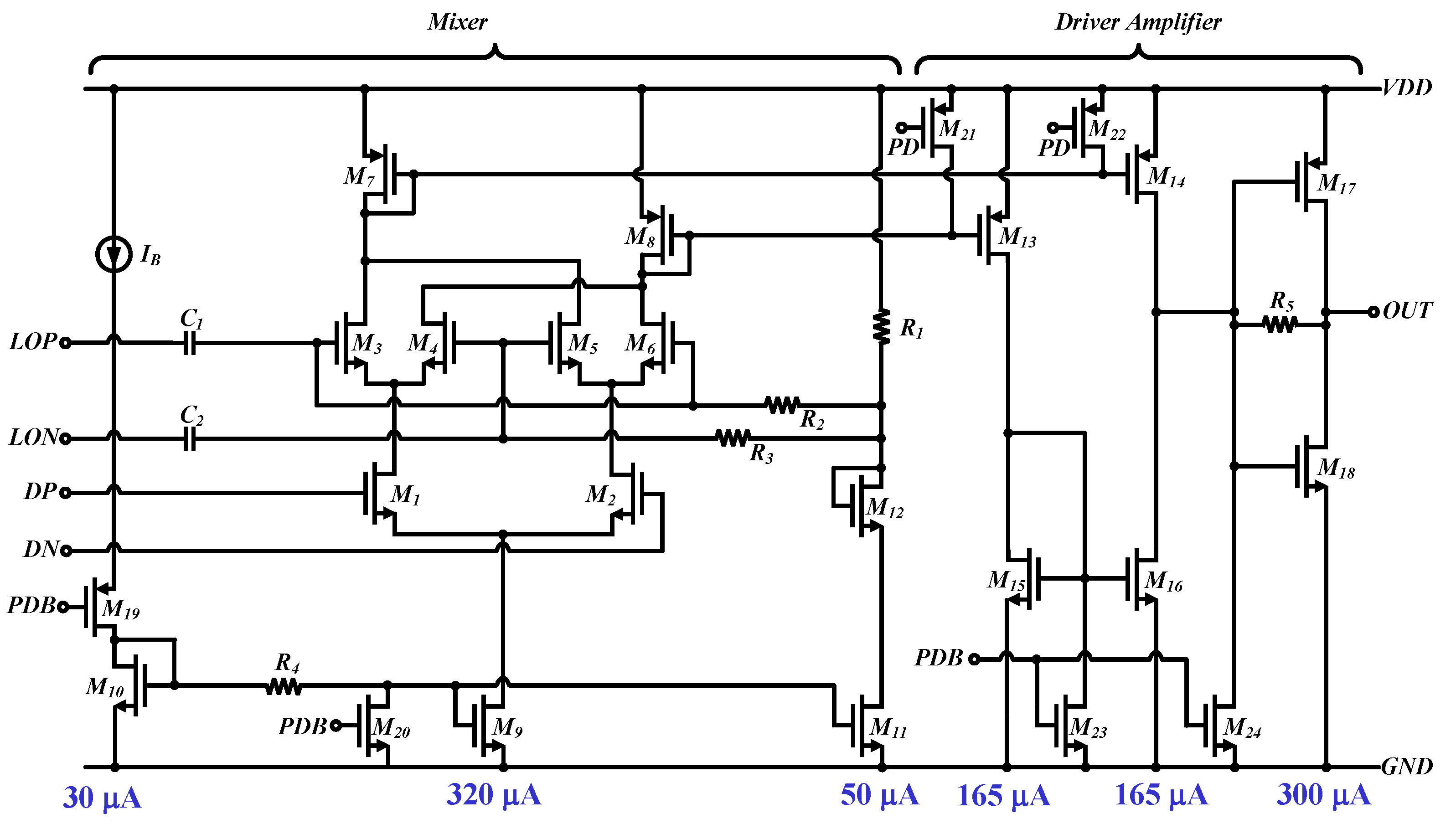
A standard transmitter RF front-end is designed, and the block diagram is shown in Figure 1. The circuits consist of an active mixer, a driver and a class-E PA. A double-balanced Gilbert active mixer is designed to realize BPSK modulation. The driver is used to preamplifiy the RF signal, and the PA adopts a parallel four-branch cascode structure to control the output power level.
2.
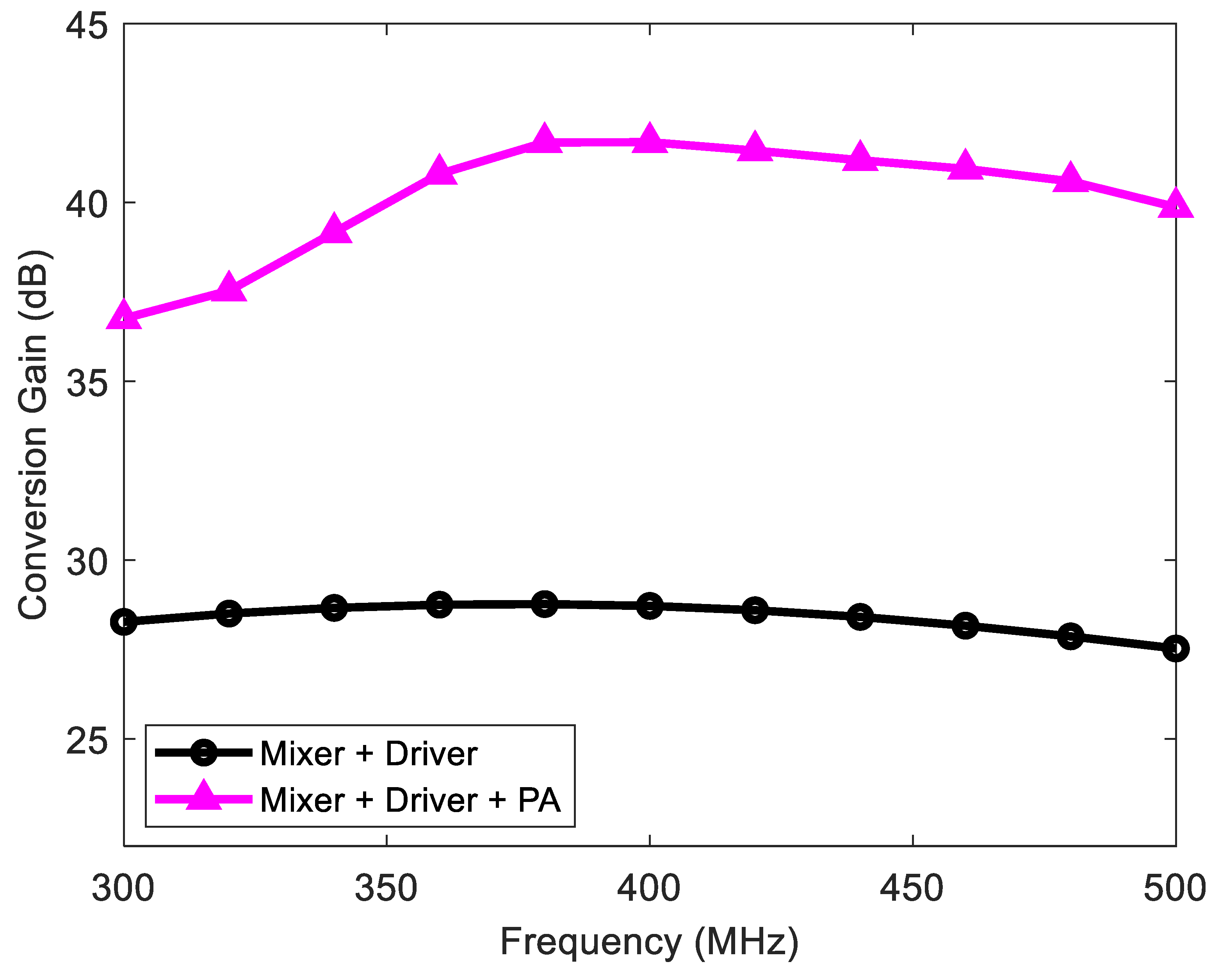
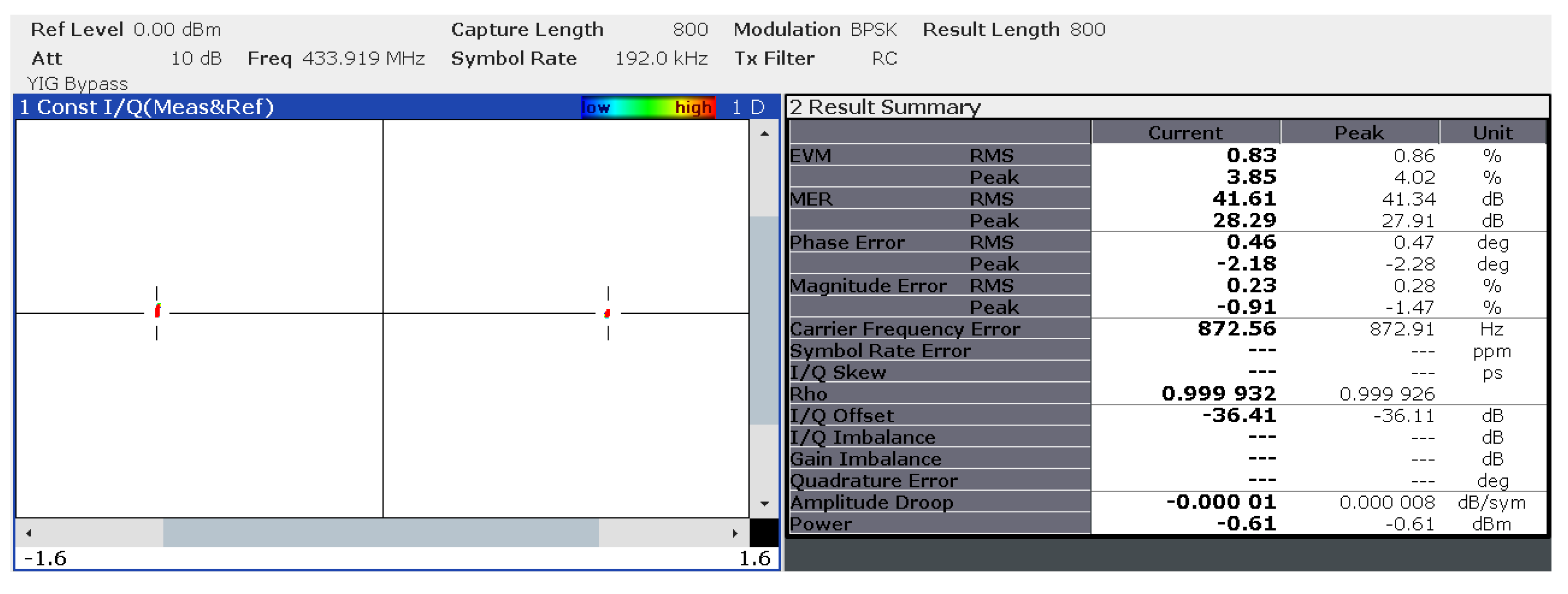
Since the transmitter RF front-end is mainly used in the transmission of digitized low-frequency signals such as voice signals, a 192 kbps data rate is selected for the transmitters. The experimental results show that the transmitter RF front-end can achieve a better error vector magnitude (EVM) when compared with similar works.
Figure 1. The block diagram of the transmitter RF front-end.
Electronics 12 04711 g001
This paper is arranged as follows: Section 2 presents the principles and analysis for the circuits. Section 3 gives the circuit design of the transmitter RF front-end. Section 4 shows the experimental results. Section 5 discusses the limitation and potential future work. Finally, conclusions are drawn in Section 6.

2. Analysis of Circuits

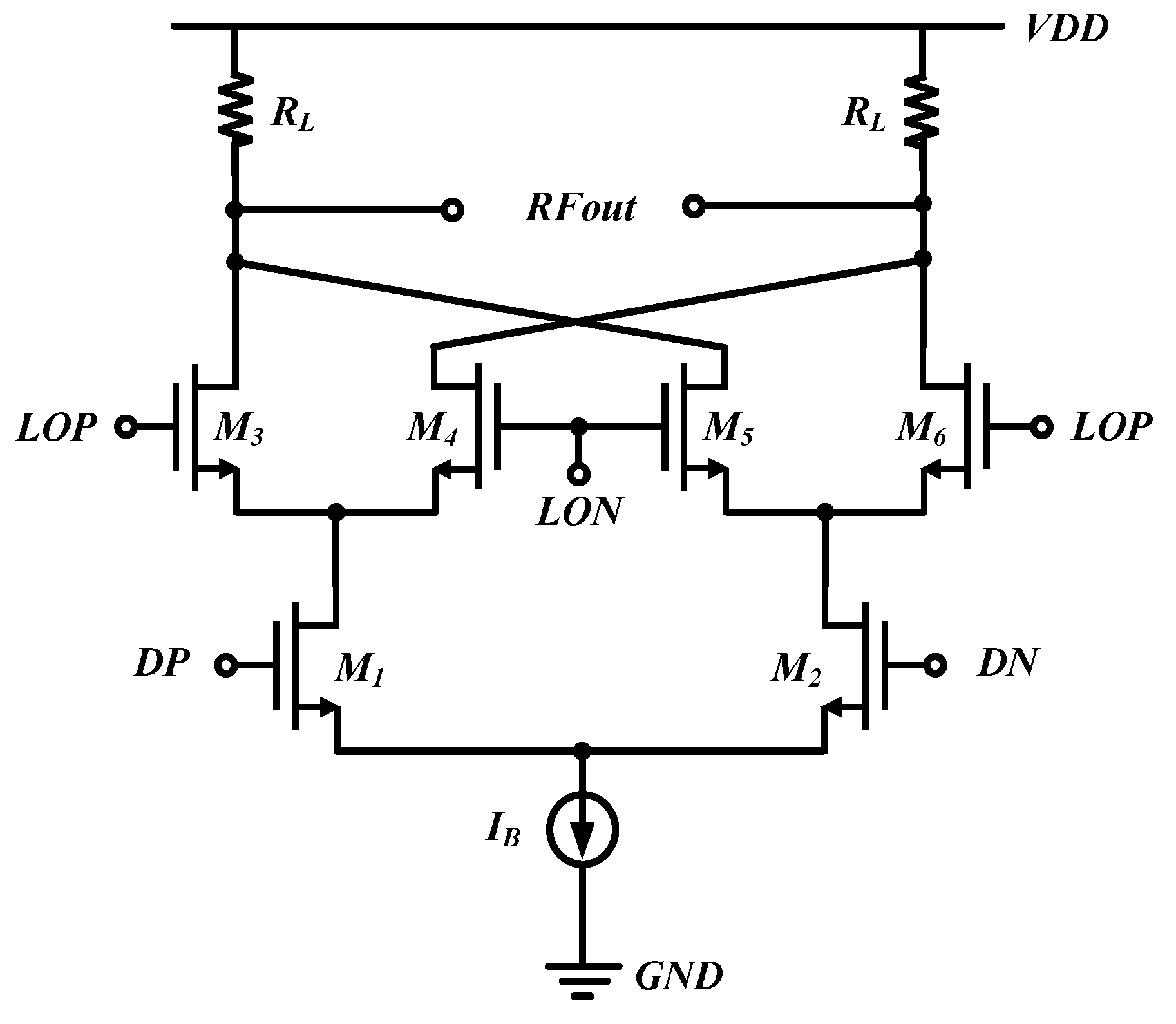
2.1. Analysis of the Gilbert Mixer

Figure 2 illustrates a simplified schematic of a double-balanced Gilbert mixer, which converts the baseband and local oscillating voltage signals to currents, mixes the currents together as RF currents and converts the RF currents to output voltages via load resistors. Since the input transconductance and output transresistance can be designed as large values, the mixer can theoretically yield an arbitrarily high gain.
L O P and L O N are the differential local oscillating signals, and D P and D N are the baseband signals, which are “1” or “0”. Therefore, the transistors M 1 M 6 operate in switching mode. Assume the waveform of the local oscillating signal is a sinusoidal signal and can be expressed as
V L O ( t ) = V L O sin ( ω L O t + θ )
where V L O , ω L O and θ are the magnitude, frequency and initial phase of the local oscillating signal, respectively. The baseband signal is the differential square signal and can be regarded as the superposition of sinusoidal waves with multiple frequency components. The baseband signal can be expressed as
V B B ( t ) = 4 π ( s i n ω B B ( t ) + 1 3 s i n 3 ω B B ( t ) + 1 5 s i n 5 ω B B ( t ) + . . . )
where ω B B represents the frequency of the baseband signal.
When M 1 turns on, the current passing through M 3 can be written as
I D ( t ) = g m V L O sin ( ω L O t + θ )
where g m is the transconductance of M 3 6 . Because M 1 and M 2 are driven by baseband square signals, they can be regarded as ideal switches. The currents passing through M 1 and M 3 are mixed together and converted to voltage signal via load resistor R L . The voltage signal can be written as
V R F ( t ) = g m V L O ( t ) V B B ( t ) R L = 2 π g m V L O R L [ c o s ( ω L O + ω B B ) t + c o s ( ω L O ω B B ) t + . . . ]
Therefore, the conversion gain of the mixer can be calculated as
C G M i x e r = V R F V L O 2 π g m R L
where V R F is the magnitude of the modulated signal. It can be seen from (5) that the modulated signal includes neither the baseband nor the local frequency components. Hence, the ideal double-balanced Gilbert mixer can effectively suppress the baseband and local signal feedthrough.

2.2. Analysis of the Class-E PA

The simplified schematic of a class-E PA is shown in Figure 3a, which consists of a transistor M 1 operating in switching mode, a choke inductor L 0 to isolate AC and DC signals, a shunt capacitor C p and a compensation inductor L x to adjust the current and voltage waveform, as well as a resonant circuit including L s and C s to select the fundamental frequency signal. The equivalent circuit diagram of Class-E PA is shown in Figure 3b, in which M 1 is replaced by an ideal switch. Assuming the switch is driven by a square wave with a duty cycle of 50%, the circuit can be divided into two modes. When the switch is closed (i.e., 0 ≤ ω t < π ), the voltage across the switch is 0 and the current is not 0. When the switch is open (i.e., π ω t < 2 π ), the current through the switch is 0 and the voltage is not 0. The current flowing through LC resonant circuit i L can be derived by
i L = I L sin ( ω t + φ )
where ω and φ are the frequency and initial phase of the driving signal. I L is the magnitude of the current flowing through LC resonant. The total currents of the switch i S W and shunt capacitor i C p can be written as
i S W + i C p = I 0 i L = I 0 I L sin ( ω t + φ )
where I 0 is the current flowing the choke inductor. When ω t ∈ [0, π ), the switch is closed, and the currents of the switch and shunt capacitor can be derived by
i S W = I 0 I L sin ( ω t + ϕ ) i C p = 0
where ϕ is the initial phase of the current flowing through LC resonant. The voltage of the switch can be written as
v S W = 0
When ω t ∈ [ π ,2 π ), the switch is open, and the current of the switch and shunt capacitor can be derived by
i S W = 0 i C p = i 0 I L sin ( ω t + ϕ )
and the voltage of the switch can be written as
v S W = v C p = 1 ω C p π ω t i C p d ( ω t ) = 1 ω C p π ω t ( I 0 I L sin ( ω t + ϕ ) ) d ( ω t )
The driver signal, current waveform and voltage waveform of the switch are shown in Figure 4. It can be seen from the figure that the current and voltage of the switch do not overlap in the time domain. As a result, the circuit has no power consumption and its efficiency can ideally be up to 100%. The ideal operating conditions for Class-E PAs are ZVS (Zero Voltage Switch) and ZVDS (Zero Voltage Derivative Switch), which can be written as
v ( ω t ) = 0 ω t ( 2 n π , ( 2 n + 1 ) π ] , n = 0 , 1 , 2 , 3 d v ( ω t ) d ω t = 0 ω t = 2 n π , n = 1 , 2 , 3
Figure 3. (a) The simplified schematic of class-E PA. (b) Equivalent circuit diagram of class-E PA.
Electronics 12 04711 g003

3. Circuit Design

As shown in Figure 1, the overall architecture includes a double-balanced Gilbert mixer, a driver and a class-E PA. The circuits are designed in a 55 nm LP CMOS process, and the supply voltage of the mixer and the driver is 1.2 V. To obtain an RF signal with a high power level, the PA adopts 1.8 V supply voltage. The design targets are listed in Table 1.
With the above design targets, this section illustrates the detailed circuits and design procedures.

3.1. Mixer and Driver Stage Circuit Design

The baseband signals need to be upconverted to RF signals by a mixer and then preamplified by a driver before they arrive at a PA. The schematic of the mixer and the driver is shown in Figure 5.
To achieve a better isolation performance, a double-balanced Gilbert mixing topology is selected. M 1 M 2 are the input transistors for the baseband signals. M 3 M 6 are the input transistors for the local oscillating signals. The signals are converted to currents, and then the currents are mixed together to form RF currents. Finally, the the RF currents are converted to output RF voltage signals via load current mirrors M 7 M 8 . M 9 provides the tail current for the Gilbert cell. M 10 M 12 and R 4 provide bias for M 3 M 6 . D P and D N are the baseband signals, which are sequences of “1” or “0”, and L O P and L O N are the differential local oscillating signals. With a baseband frequency of f B B and a local frequency of f L O , an output frequency f R F = f L O ± f B B can be achieved.
The driver stage includes a differential to single-ended transformation circuit, which is composed of transistors M 13 M 16 , and a driving buffer consisting of M 17 M 18 and R 5 . Meanwhile, several switching transistors, including M 19 M 24 , are used to reduce power consumption when the system is idle. P D and P D B are control signals which turn on or off the corresponding transistors. When P D = 0 and P D B = 1 , the corresponding branches are turned off.
To meet the design specification, the conversion gain of the mixer and the voltage gain of the driver are set to about 15 dB and more than 10 dB, respectively. Their power consumption is set to less than 1.3 mW. Based on Equation (5), the conversion gain of the mixer is
C G M i x e r = 2 π g m 3 g m 7
Therefore, g m 3 ≈ 6· g m 7 . The bias current of each branch is allocated as Figure 5 shows, and the initial size of each transistor can be calculated by I V equations of the transistor. After adjusting the parameters to meet the PVT variation, the final component parameters are listed in Table 2.

3.2. Class-E PA Circuit Design

The schematic of the class-E PA is shown in Figure 6, in which four parallel cascode branches are used to control the output power level of the PA [20,21]. Common source transistors M 1 M 4 with a thin oxide layer are driven by the signal from the driver stage and operate in switching mode. Common gate transistors M 5 M 8 with a thick oxide layer are employed to improve reliability at high voltages. To control the level of output power, the common gate transistors are controlled by a four-bit power control word (PCW). P A I N is the driving signal from the previous driver, and its waveform is similar to square wave, as shown in Figure 4. P D B is the switching signal for the PA. When P D B = 1 , all the currents will be set to 0 and the PA will turn off. The design procedure of the PA includes two phases, which are circuit stage design and resonant and matching network design. Since the output power range is set to be from −6 dBm to 3 dBm, the currents of the four branches are set to 100 μ A, 50 μ A, 50 μ A and 100 μ A, respectively. The sizes of the transistors are listed in Table 3.
As the PA operates in 433 MHz frequency, the resonant and matching network is realized by off-chip components. The output network includes an off-chip choke inductor L 0 to isolate AC and DC signals and a shunt capacitor C p and a compensation inductor L x to adjust the current and voltage waveform, as well as a resonant circuit including L s and C s to select the fundamental frequency signal.
To reduce power loss, a load network with a 500 nH finite DC-feed inductor is employed in the Class-E PA. Calculated parameters of the passive devices are shown in Table 4, where R L is an ideal load of 250 Ω . To match the actual load of a 50 Ω antenna and achieve the maximum power transmission, an L-type impedance matching network, as shown in Figure 6, is employed, and Figure 7 illustrates the matching process using a Smith Chart. As Figure 7a shows, the load–pull simulation scans out the transmitted power for multiple impedance values of the actual load. Each circle represents an equal power level, where the star-shaped point ( P 1 ) is the impedance point of maximum power transmission. Relevant studies have proven that conjugate matching is a condition for maximum power transmission [22,23,24,25]. The matching procedure is shown in Figure 7b. First, a capacitor is paralleled in the circuit to lead the matching path following the black line ( P a t h 1 ). Second, an inductor is connected in series, and the matching path is the red line ( P a t h 2 ).
Finally, since the mixer and the driver work with a 1.2 V supply voltage and the class-E PA operates with a 1.8 V supply voltage, they are integrated into a single chip but are separated to two voltage domains by Deep Nwells [26,27].

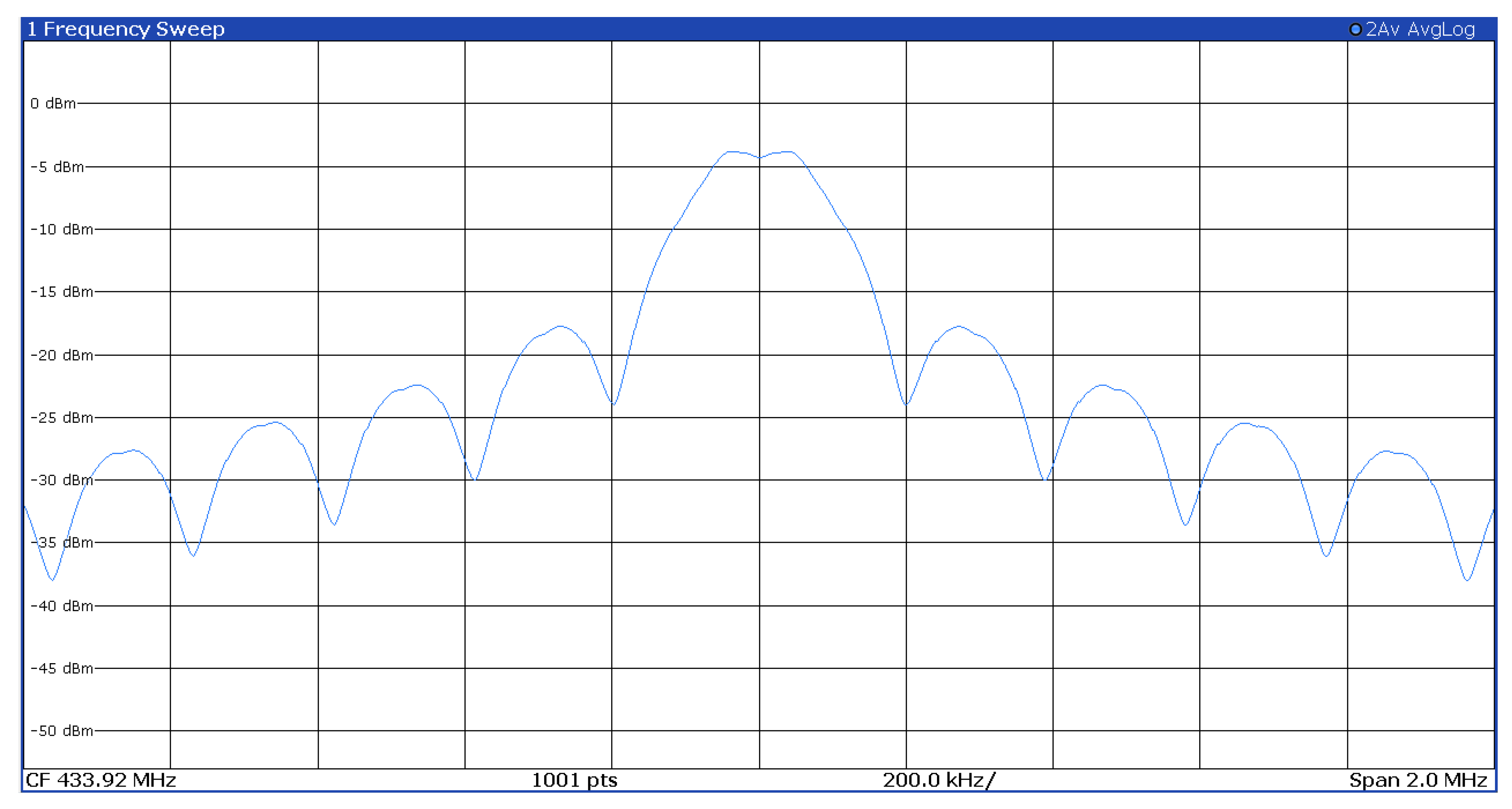
4. Experimental Results

The transmitter RF front-end is fabricated in a 55 nm CMOS LP process. The chip microphotograph and the corresponding layout are shown in Figure 8. The area of the chip is about 0.018 mm 2 . To guarantee the function the proposed transmitter RF front-end, a postlayout simulation is performed. Figure 9 gives the conversion gain of the circuits. With a local oscillating signal whose power is −20 dBm, it can be seen from this figure that the mixer and the driver provide a conversion gain of about 28.5 dB, and the transmitter RF front-end has a total conversion gain of about 41.3 dB at the 433.92 MHz frequency. The output powers with different PCW are shown in Figure 10. The maximum output power is more than 3.2 dBm over a power range from −26 dBm to −15 dBm. Additionally, the postlayout simulated stability factors B 1 f and K f are shown in Figure 11. It can be seen from the figure that B 1 f > 0 and K f > 1 at 433 MHz frequency, which means that the PA is stable.
After tapeout and packaging, the chip is bonded to a PCB board and tested. With a 200 mVpp and 433.92 MHz frequency sinusoidal signal at the local oscillating signal port, as well as a 1.2 V DC signal at the baseband port, the output spectrum with maximum output power level is shown in Figure 12. It can be seen from the figure that the maximum output power is 2.7 dBm.
The performance DE reflects the efficiency of the PA, and it is defined as
D E = P o u t P s u p p l y
Figure 13 plots the postlayout simulated and measured maximum output power and DE of the class-E PA over the frequency range of 400 MHz∼500 MHz. We can find that the postlayout simulated maximum output power and DE at 433.92 MHz frequency are 3.7 dBm and 40.1%, respectively, while the measured maximum output power and DE at 433.92 MHz frequency are 2.7 dBm and 34.5%, respectively.
We also tested the S 22 of the output port, and the measured result is shown in Figure 14. We can find that S 22 is less than −10 dB in the 393.79 MHz∼455.70 MHz frequency range.
With a 192 kbps input signal, the output BPSK spectrum is shown in Figure 15. The bandwidth of the output signal is about 384 kHz. The measured EVM is shown in Figure 16. We can find that the measured EVM is about 0.83% rms, and the magnitude error and the phase error are 0.23% and 0.46 , respectively.
Furthermore, the measured power consumption of the whole chip is about 6.72 mW, among which the mixer and driver consume about 1.32 mW, and the class-E PA consumes about 5.4 mW.
We summarized the measurement results, and the performance comparison is shown in Table 5. It can be seen from the table that the proposed transmitter RF front-end can achieve a better EVM when compared with similar works.

5. Discussion

Since the main purpose of this work is to verify the feasibility of utilizing a low-power digital process for a potential mixed-signal design, only a few key analog/RF blocks were integrated to form the backbone of the transmitter. Other blocks, such as a phase lock loop, amplifiers and an analog-to-digital converter, which are needed for a standalone transmitter with sensing function, are omitted in this version of the design. Meanwhile, each block of this work is a standard implementation of corresponding architecture without the latest performance improvement techniques. Additionally, to suppress the local oscillating feedthrough, various methods are proposed by integrating an upsample filter and designing calibration schemes [30,31,32]. All of the above points could be improved in future works.

6. Conclusions

This paper presented a 433 MHz transmitter TX front-end with a double-balanced active mixer and a class-E PA using a 55 nm CMOS LP process. A driver was designed to preamplify the RF signal before the PA. The chip occupies an area of 0.018 mm 2 , and the total power consumption is about 6.72 mW. The measured results show that the performances of the transmitter TX front-end can meet the requirements of BPSK transmitters with moderate data rates.

Author Contributions

Conceptualization, Y.W. and H.X.; methodology, H.Y., R.Z. and H.X.; formal analysis, H.Y., R.Z. and P.W.; validation, H.Y., R.Z. and P.W.; writing—original draft preparation, H.Y. and R.Z.; writing—review and editing, all authors; visualization, H.Y., R.Z. and P.W.; supervision, H.X. and Y.W.; project administration, Y.W.; funding acquisition, Y.W. All authors have read and agreed to the published version of the manuscript.

Funding

This research was funded in part by the National Key Research and Development Program of China under grant 2021YFA1003600, and in part by the Natural Science Foundation of Shandong Province under grant ZR2023ZD07 and ZR2022MF316.

Institutional Review Board Statement

Not applicable.

Data Availability Statement

Data are contained within the article.

Conflicts of Interest

The authors declare no conflict of interest.

References

  1. Liu, C.; Shi, C.J.R. Design of the class-E power amplifier considering the temperature effect of the transistor on-resistance for sensor applications. IEEE Trans. Circuits Syst. II Express Briefs 2021, 68, 1705–1709. [Google Scholar] [CrossRef]
  2. Wang, Y.; Zhou, R.; Liu, Z.; Yan, B. A low-power CMOS wireless acoustic sensing platform for remote surveillance applications. Sensors 2020, 20, 178. [Google Scholar] [CrossRef]
  3. Seneviratne, S.; Hu, Y.; Nguyen, T.; Lan, G.; Khalifa, S.; Thilakarathna, K.; Hassan, M.; Seneviratne, A. A survey of wearable devices and challenges. IEEE Commun. Surv. Tutorials 2017, 19, 2573–2620. [Google Scholar] [CrossRef]
  4. Verma, N.; Hu, Y.; Huang, L.; Rieutort-Louis, W.S.; Robinson, J.S.; Moy, T.; Glisic, B.; Wagner, S.; Sturm, J.C. Enabling scalable hybrid systems: Architectures for exploiting large-area electronics in applications. Proc. IEEE 2015, 103, 690–712. [Google Scholar] [CrossRef]
  5. Liu, B.; Yi, X.; Yang, K.; Liang, Z.; Feng, G.; Choi, P.; Boon, C.C.; Li, C. A carrier aggregation transmitter front end for 5-GHz WLAN 802.11ax application in 40-nm CMOS. IEEE Trans. Microw. Theory Tech. 2020, 68, 264–276. [Google Scholar] [CrossRef]
  6. Wang, X.; Jin, J.; Liu, X.; Zhou, J. An ISM band high-linear current-reuse up-conversion mixer with built-in-self-calibration for LOFT and I/Q imbalance. IEEE Trans. Circuits Syst.-Express Briefs 2020, 67, 2898–2920. [Google Scholar] [CrossRef]
  7. Handel, P.; Ronnow, D. Modeling mixer and power amplifier impairments. IEEE Microw. Wirel. Compon. Lett. 2019, 29, 441–443. [Google Scholar] [CrossRef]
  8. Voltti, M.; Koivisto, T.; Tiiliharju, E. Comparison of active and passive mixers. In Proceedings of the 2007 18th European Conference on Circuit Theory and Design, Seville, Spain, 27–30 August 2007; IEEE: New York, NY, USA, 2007; pp. 890–893. [Google Scholar]
  9. Li, J.; Gu, Q.J. Harmonic-based nonlinearity factorization of switching behavior in up-conversion mixers. IEEE Trans. Circuits Syst. I Regul. Pap. 2019, 66, 2468–2477. [Google Scholar] [CrossRef]
  10. Li, Z.; Torfs, G.; Bauwelinck, J.; Yin, X.; Vandewege, J.; Praet Van, C.; Spiessens, P.; Tubbax, H.; Stubbe, F. A 2.45-GHz +20-dBm fast switching class-E power amplifier with 43% PAE and a 18-dB-wide power range in 0.18-um CMOS. IEEE Trans. Circuits Syst. Express Briefs 2012, 59, 224–228. [Google Scholar] [CrossRef]
  11. Ponte, J.; Ghahremani, A.; Huiskamp, M.; Annema, A.J.; Nauta, B. Theory and implementation of a load-mismatch protective class-E PA system. IEEE Trans. Circuits Syst. I Regul. Pap. 2020, 67, 369–377. [Google Scholar] [CrossRef]
  12. Yang, C.; Jin, K.; Mao, D.; Zhu, X. Precise configuration of transmission line Class-E power amplifier operating at GHz Frequency. IEEE J. Emerg. Sel. Top. Power Electron. 2022, 10, 6396–6404. [Google Scholar] [CrossRef]
  13. Yang, Z.; Li, M.; Dai, Z.; Xu, C.; Jin, Y.; Li, T.; Tang, F. A generalized high-efficiency broadband class-E/F-3 power amplifier based on design space expanding of load network. IEEE Trans. Microw. Theory Tech. 2020, 68, 3732–3744. [Google Scholar] [CrossRef]
  14. Yi, K.S.; Murad, S.A.Z.; Mohyar, S. A study and analysis of high efficiency CMOS power amplifier for IoT applications. In Proceedings of the Journal of Physics: Conference Series, 5th International Conference on Electronic Design (ICED), Perlis, Malaysia, 19 August 2020; IOP Publishing: Bristol, UK, 2021; Volume 1755, p. 012020. [Google Scholar]
  15. Mindubaev, E.; Danilov, A. Effect of class E power amplifier loading network on output power and efficiency of inductive powering system for implantable medical devices. In Proceedings of the AIP Conference Proceedings, St. Petersburg, Russia, 3–6 July 2019; AIP Publishing LLC.: Melville, NY, USA, 2019; Volume 2140, p. 020046. [Google Scholar]
  16. Latha, Y.M.A.; Rawat, K. Extending the design space of class E mode to design a multi-octave power amplifier. IEEE Trans. Circuits Syst. II Express Briefs 2022, 69, 4829–4833. [Google Scholar]
  17. Du, J.C.; Wang, Z.G.; Xu, J.; Yang, Y.F. A Current-Injection Class-E Power Amplifier. IEEE Microw. Wirel. Components Lett. 2020, 30, 775–778. [Google Scholar] [CrossRef]
  18. Milosevic, D.; van der Tang, J.; Van Roermund, A. Explicit design equations for class-E power amplifiers with small DC-feed inductance. In Proceedings of the 2005 European Conference on Circuit Theory and Design, Cork, Ireland, 2 September 2005; IEEE: New York, NY, USA, 2005; Volume 3, pp. III/101–III/104. [Google Scholar]
  19. Acar, M.; Annema, A.J.; Annema, A.J. Analytical design equations for Class-E power amplifiers. IEEE Trans. Circuits Syst. I Regul. Pap. 2007, 54, 2706–2717. [Google Scholar] [CrossRef]
  20. Mazzanti, A.; Larcher, L.; Brama, R.; Svelto, F. Analysis of reliability and power efficiency in cascode class-E PAs. IEEE J. Solid-State Circuits 2006, 41, 1222–1229. [Google Scholar] [CrossRef]
  21. Kutty, K. Class-E Cascode Power Amplifier Analysis and Design for Long Term Reliability. 2010. Available online: http://purl.fcla.edu/fcla/etd/CFE0003360 (accessed on 25 June 2023).
  22. Rahola, J. Power waves and conjugate matching. IEEE Trans. Circuits Syst. II Express Briefs 2008, 55, 92–96. [Google Scholar] [CrossRef]
  23. Presas, S.M.; Weller, T.M.; Silverman, S.; Rakijas, M. High efficiency diode doubler with conjugate-matched antennas. In Proceedings of the 2007 European Microwave Conference, Munich, Germany, 9–12 October 2007; IEEE: New York, NY, USA, 2007; pp. 250–253. [Google Scholar]
  24. Liew, Y.H.; Joe, J. RF and IF ports matching circuit synthesis for a simultaneous conjugate-matched mixer using quasi-linear analysis. IEEE Trans. Microw. Theory Tech. 2002, 50, 2056–2062. [Google Scholar] [CrossRef]
  25. Sun, Y.; Fidler, J. Design method for impedance matching networks. IEE Proc. Circuits Devices Syst. 1996, 143, 186–194. [Google Scholar] [CrossRef]
  26. Rezvani, G.A.; Tao, J. Substrate isolation in 0.18 um CMOS technology. In Proceedings of the 2005 International Conference on Microelectronic Test Structures, 2005. ICMTS 2005, Leuven, Belgium, 4–7 April 2005; IEEE: New York, NY, USA, 2005; pp. 131–136. [Google Scholar]
  27. Wang, Z.; Cheng, G.; Kang, W.; Li, Z.; Chen, J. High isolation and high power of 0.13 um CMOS SPDT switch using deep-N-well transistors and floating-body technique in K-band. Microw. Opt. Technol. Lett. 2023, 65, 2126–2131. [Google Scholar] [CrossRef]
  28. Zong, P.; Zhou, Y.; Zhang, H.; Zhou, Y.; Wang, K. A 433 MHz transmitter based on injection-locking and frequency multiplication. In Proceedings of the 2019 IEEE 4th International Conference on Integrated Circuits and Microsystems (ICICM), Beijing, China, 25–27 October 2019; IEEE: New York, NY, USA, 2019; pp. 1–4. [Google Scholar]
  29. Vasilakopoulos, K.; Liscidini, A. A reconfigurable passive switched-capacitor TX RF front end with -57 dB ACLR2. IEEE Solid-State Circuits Lett. 2020, 3, 294–297. [Google Scholar] [CrossRef]
  30. Mohr, B.; Mueller, H.J.; Zhang, Y.; Thiel, B.; Negra, R.; Heinen, S. A digital centric CMOS RF transmitter for multistandard multiband applications. In Proceedings of the 2014 IEEE Radio Frequency Integrated Circuits Symposium, Tampa, FL, USA, 1–3 June 2014; IEEE: New York, NY, USA, 2014; pp. 221–224. [Google Scholar]
  31. Lopelli, E.; Spiridon, S.; Tang, v.d.J. A 40nm wideband direct-conversion transmitter with sub-sampling-based output power, LO feedthrough and I/Q imbalance calibration. In Proceedings of the 2011 IEEE International Solid-State Circuits Conference, San Francisco, CA, USA, 20–24 February 2011; IEEE: New York, NY, USA, 2011; pp. 424–426. [Google Scholar]
  32. Un, K.F.; Yu, W.H.; Cheang, C.F.; Qi, G.; Mak, P.I.; Martins, P.R. Sub-GHz wireless transmitter utilizing a multi-class-linearized PA and time-Domain wideband-auto I/Q-LOFT calibration for IEEE 802.11af WLAN. IEEE Trans. Microw. Theory Tech. 2015, 63, 3228–3241. [Google Scholar] [CrossRef]
Figure 2. The schematic of a simplified Gilbert mixer.
Electronics 12 04711 g002
Figure 4. The driver signal, current waveform and voltage waveform of the switch.
Electronics 12 04711 g004
Figure 5. The schematic of the active mixer and driver.
Electronics 12 04711 g005
Figure 6. The gain-controlled PA circuit.
Electronics 12 04711 g006
Figure 7. (a) The power circle chart of load-pull simulation. (b) The impedance matching process.
Electronics 12 04711 g007
Figure 8. (a) The chip microphotograph. (b) The corresponding layout.
Electronics 12 04711 g008
Figure 9. The postlayout simulated conversion gain.
Electronics 12 04711 g009
Figure 10. The postlayout simulated output powers of PA with different power control words.
Electronics 12 04711 g010
Figure 11. (a) The postlayout simulation result of B 1 f . (b) The postlayout simulation result of K f .
Electronics 12 04711 g011
Figure 12. The measured output signal power spectrum.
Electronics 12 04711 g012
Figure 13. The postlayout simulated and measured output power and DE.
Electronics 12 04711 g013
Figure 14. The measured S 22 of the output port.
Electronics 12 04711 g014
Figure 15. The measured power spectrum with 192 kbps BPSK modulation.
Electronics 12 04711 g015
Figure 16. The measured 192 kbps BPSK modulation EVM.
Electronics 12 04711 g016
Table 1. The design targets.
Design ParameterValue
Technology55 nm
Supply Voltage1.2/1.8 V
Operating Frequency433.92 MHz
Data Rate192 kbps
Overall Conversion Gain>40 dB
Power Consumption<6 mW
Maximum Output Power>3 dBm
Table 2. Component Values.
ComponentValueComponentValue
M 1 2 16 μ m/0.06 μ m M 3 6 2 × (16 μ m/0.06 μ m)
M 7 8 4 × (32 μ m/0.5 μ m) M 9 12 × (12 μ m/1 μ m)
M 10 12 μ m/1 μ m M 11 2 × (12 μ m/1 μ m)
M 12 4 × (4 μ m/0.1 μ m) M 13 14 20 μ m/0.1 μ m
M 15 16 4 × (32 μ m/0.5 μ m) M 17 2 × (64 μ m/0.06 μ m)
M 18 2 × (16 μ m/0.06 μ m) R 1 2 10 k Ω
R 3 10 k Ω R 4 6 k Ω
R 5 10 k Ω C 1 2 800 fF
Table 3. Transistor sizes of the class-E PA.
ComponentValue
M 1 4 2 × (20 μ m/0.2 μ m)
M 5 5 × (5 μ m/0.3 μ m)
M 6 2 × (2 μ m/0.3 μ m)
M 7 4 × (2 μ m/0.3 μ m)
M 8 9 × (2 μ m/0.3 μ m)
M 9 2 × (20 μ m/0.2 μ m)
Table 4. The calculated results of passive devices.
ComponentValue
C p 437 fF
R L 250 Ω
L p 74.8 nH
Table 5. Performance summary and comparison.
Performance[2][28] *[29]This Work
Year2020201920202023
ArchitectureAMP + ADC + PLLRingSRAM + DAC + PLLMixer +
+ Mixer + PAOscillator+ Mixer + DriverDriver + PA
Modulation TypeBPSKFSK64-QAMBPSK
Technology (nm)3501806555
Operating Frequency4334331000433
(MHz)
VDD (V)1.8/2.51.8N.A.1.2/1.8
DE (%)N.A.N.A.N.A.34.5
Maximum Pout5.7−289.52.7
(dBm)
Area (mm 2 ) 1.710.00180.50.018
Power (mW)25.1 (PA 9.8)0.58456.72
Bandwidth (MHz)0.384N.A.200.384
EVM (%)17.06N.A.7.330.83
* Postlayout simulation.
Disclaimer/Publisher’s Note: The statements, opinions and data contained in all publications are solely those of the individual author(s) and contributor(s) and not of MDPI and/or the editor(s). MDPI and/or the editor(s) disclaim responsibility for any injury to people or property resulting from any ideas, methods, instructions or products referred to in the content.

