Article

Design of a 7.5 kW Dual Active Bridge Converter in 650 V GaN Technology for Charging Applications

1
Department of Electrical, Electronic, and Information Engineering “Guglielmo Marconi”, University of Bologna, 40136 Bologna, Italy
2
OCEM Power Electronics, 40056 Valsamoggia, Italy
*
Author to whom correspondence should be addressed.
Submission received: 15 January 2023 / Revised: 2 March 2023 / Accepted: 6 March 2023 / Published: 7 March 2023

Abstract

:
High-voltage GaN switches offer low conduction and commutation losses compared with their Si counterparts, enabling the development of high-efficiency switching-mode DC–DC converters with increased switching frequency, faster dynamics, and more compact dimensions. Nonetheless, the potential of GaN switches can be fully exploited only by means of accurate simulations, optimal switch driving, suitable converter topology, accurate component selection, PCB layout optimization, and fast digital converter control. This paper describes the detailed design, simulation, and implementation of an air-cooled, 7.5 kW, dual active bridge converter exploiting commercial 650 V GaN switches, a compact planar transformer, and low ESL/ESR metal film capacitors. The isolated bidirectional converter operates at a 200 kHz switching frequency, with an output voltage range of 200–500 V at nominal 400 V input voltage, and a maximum output current of 28 A, with a wide full-power ZVS region. The overall efficiency at full power is 98.2 % . This converter was developed in particular for battery charging applications, when bidirectional power flow is required.

1. Introduction

The trend in automotive power-train electrification has drastically sped up in the recent years, motivated by enormous industrial investments in response to the demanding environmental requirements imposed by legislators and the growing appeal of electric and hybrid vehicles among the population [1]. One of the most thriving topics concerns the charging framework used for automotive electric energy storage (EES), typically lithium-ion battery packs, in which OFF/ON board chargers play the main role. These are usually two-stage systems, with an AC/DC grid-tied converter and a DC–DC converter to regulate the battery voltage and current, where increased efficiency and bidirectionality are required, respectively, to reduce the system size and for vehicle-to-grid (V2G) power flow. Concerning the DC section, among the different topologies investigated [2,3], the most promising are the CLLC [4] and dual active bridge (DAB) [5] isolated converters. Despite the CLLC converter guaranteeing a slightly higher efficiency and better light-load management than DAB, the latter still provides excellent performance with a shorter component list, a simpler control mechanism owing to a fixed switching frequency, and a wider output voltage range to cope with different battery types. On the other hand, wide band-gap (WBG) technology, using materials such as silicon carbide (SiC) and gallium nitride (GaN), is gaining a considerable share of the market to the detriment of Si devices. For LEVEL3 chargers [6], only SiC transistors can be exploited for the higher breakdown voltages and longer heritage; in the LEVEL2 range (1.8–19.2 kW), commercial 650 V GaN technology solutions are available for power electronic applications owing to normally OFF HEMT devices. The superior characteristics in terms of low channel resistance for current capability, small capacitive parasitics, and absence of reverse recovery charge are crucial to increase efficiency, power density, and switching frequency, enabling the shrinking of the magnetic components such as the high-frequency transformer, which is typically one of the bulkiest device in the DAB topology. However, such benefits come along with new challenges from the design point of view: the elevated d i d t , d v d t must be handled in terms of layout, minimizing inductive loops with a wise signal and ground plane arrangement, and adopting suitable components for the high-frequency regime with reduced stray inductances.
Some design examples can be found in the literature, where DAB topology and GaN technology are jointly exploited. In [7], a 4 kW DAB/GaN converter is described for electric aircraft with peak efficiency ranging from 96 % to 98 % at a 100 KHz switching frequency. In [8], a 3 kW DAB/GaN converter operating at 100 KHz is described for aircraft applications reaching up to 95.5 % peak efficiency. The DAB/GaN converters described in [9,10,11] for battery charging applications deliver 3.7 kW, 3.7 kW, and 2.4 kW at a 500 KHz switching frequency and 98.7 % , 95.7 % , and 96.4 % peak efficiencies, respectively.
In this context, a 7.5 kW DAB converter operating at a 200 kHz switching frequency using 650 V commercial HEMT GaN transistors suitable for charging applications was designed and implemented in this study. The design exploited the PSIM [12] simulation environment for electrical and thermal simulations. Power and control printed circuit boards (PCBs) were designed using the Eagle CAD tool [13] by Autodesk. In Section 2, the DAB converter working principles are explained; in Section 3, the design procedure of the prototype is described; in Section 4, the realized converter is shown along with results of the experimental tests.

2. Topology

A schematic of a DAB converter is shown in Figure 1: two full bridges (FBs) are connected at the primary and secondary side to a high-frequency transformer with a series input inductor that provides energy storage. The two FBs typically operate at a fixed switching frequency and 50 % duty cycle, and the power flow is controlled by regulating the voltage applied to the series inductor by adjusting the time displacement (phase shift) among the gate signals of the two FBs. The symmetrical structure enables bidirectionality, whereas the wide voltage range generation (either in buck or boost mode) is guaranteed by the possibility of alternatively imposing the sum and difference of the input/output voltages across the inductor. The fundamental law of a DAB converter is retrievable analyzing the waveforms in Figure 2. For the sake of clarity, steady-state operations, constant input and output voltages, the absence of a transformer, and single phase-shift (SPS) modulation are assumed. SPS means that the devices within the same FB are ON for half a period at fixed diagonals (for instance, Q1–Q4 share the same gate signal as well as Q2–Q3), while the useful phase-shift lies on the gate signals of devices with different FBs.
Looking at Figure 2 from top to bottom, the following waveforms can be observed, respectively: the gate signals of Q1 and Q5, the high-frequency voltage waveforms V 1 , V 2 , and the inductor voltage and current V L , I L . The time period T s is divided into four slots. Focusing on the inductor current, the equations for the first two time slots follow [14]
i L ( ϕ ) = i L ( 0 ) + Δ I 1 Δ I 1 = V 1 + V 2 L ϕ T s 2 π = V 1 + V 2 2 π f s L ϕ
i L ( π ) = i L ( ϕ ) + Δ I 2 Δ I 2 = V 1 V 2 L ( π ϕ ) T s 2 π = V 1 V 2 2 π f s L ( π ϕ )
where ϕ is the phase shift between gate signals Q1 and Q5.
Because, in the steady state, the average inductor current over the period is null and owing to the symmetrical FB mode of operation, every inductor current value is repeated after a half period with the opposite sign, in particular:
i L ( π ) = i L ( 0 ) + Δ I 1 + Δ I 2 = i L ( π ) + Δ I 1 + Δ I 2
Substituting and rearranging Equations (1)–(3), the results are:
i L ( π ) = V 1 π + V 2 ( 2 ϕ π ) 4 π f s L
i L ( ϕ ) = V 2 π + V 1 ( 2 ϕ π ) 4 π f s L
where Equations (4) and (5) are, respectively, the peak of I L in buck and boost modes. At the input and output ports of the converter, the inductor current is rectified by FBs every half period; therefore, the main harmonic component occurs at 2 f s , and the power can be computed taking into account only a half period.
P = P o u t = P i n = V 1 1 π 0 π i L ( θ ) d θ = V 1 π 0 ϕ i L ( θ ) d θ + ϕ π i L ( θ ) d θ = V 1 π ϕ ( i L ( ϕ ) i L ( 0 ) ) 2 + ( π ϕ ) ( i L ( π ) i L ( ϕ ) ) 2 = V 1 V 2 2 π 2 f s L ϕ ( π ϕ )
Finally considering the turn ratio n = N 2 / N 1 and the possibility of having a negative ϕ (i.e., the gate signal of Q 5 precedes that of Q 1 ), Equation (6) becomes
P = n V 1 V 2 2 π 2 f s L ϕ ( π | ϕ | )
where π / 2 < ϕ < π / 2 because the maximum power in absolute terms is obtained for ϕ = π / 2 :
| P m a x | = n V 1 V 2 8 f s L
The DAB converter allows us to obtain ZVS owing to the inductance L that acts as a current generator, charging and discharging the devices’ output capacitances during dead time. Figure 3 shows what happens during dead time when Q1–Q4 are set OFF and Q2–Q3 are set ON for the FB at the primary side. The inductor forces a current that discharges C o s s of Q2 and Q3 while charging Q1 and Q4. When the energy of output capacitances is over, the devices proceed in reverse conduction, acting as free-wheeling diodes, enabling the activation of Q2 and Q3 with an almost null drain-source voltage. This practically eliminates the switching losses at turn ON. ZVS operation is assured when Equations (4) and (5) are both positive [15] and when the power balance
1 2 L i L 2 > 4 1 2 C o s s V 2
is fulfilled. Equation (9) is valid in most of the conditions, in particular with WBG devices with low parasitics. The conditions on I L ( π ) and I L ( ϕ ) are used to delimit the ZVS region.
Looking at Equation (7), there are three main components that determine the power delivery: the switching frequency f S , phase shift ϕ , and inductance L. The major effect of ϕ and L reflexes on the current level [16] are as follows: an increasing phase shift reflects a higher current when voltages are fixed; the same result can be obtained with a larger inductance due to an increased energy storage capability. Such behavior leads to a wider ZVS region but also to higher RMS currents. Indeed, one disadvantage of DAB converters in SPS mode is the high level of RMS current on DC-link capacitors because of the lack of inductive filtering in the input and output sections. This can be mitigated by exploiting different modulation techniques such as the dual phase shift (DPS) [17], which also acts on the duty cycle of the transistor diagonals within the same FB, but this was beyond the scope of this study. The f S has a huge impact on the size of the magnetic components, in particular on high-frequency transformers. Nonetheless, at high switching frequencies, the accurate selection of core and winding technology and techniques is fundamental to avoid performance degradation due to excessive losses and large/uncontrolled parasitic effects. In this context, planar transformer technology is an attractive solution for its ability to obtain a small form factor, better power dissipation, and accurate prediction and repeatability of parasitics. The latter is a significant advantage because, at high frequency, parasitics play a fundamental role in the actual operation of the converter, for example, in the ZVS mechanism described before, where the leakage inductance of the transformer is a key parameter, which must then be accurately known and must be highly repeatable in the transformer construction.

3. Converter Design

3.1. Dimensioning

In Table 1, the proposed specifications for the DAB converter are illustrated. The indicated high target value for the switching frequency f s = 200 kHz that would enable high power density, as discussed, can be addressed for these voltage and current ratings only by exploiting WBG semiconductor technologies to limit the switching losses and to enable higher operating temperatures. In Table 2, a short list of commercially available WBG devices that are potentially suitable for the design goals in Table 1 is shown. GS66516B [18] provides the best performance in terms of parasitics and maximum current level; in particular, the null reverse recovery charge of GaN devices is achieved due to the absence of a body diode, which typically allows them to work at higher frequencies than SiC transistors. GaN switching time is shorter due to its much lower input capacitance. Moreover, the high-frequency design of the GS66516B leadless package guarantees minimal stray inductance, facilitating the minimization of the switching time. The GS66516B device was adopted to implement the two full bridges of the converter. With the following calculations and simulations, it is demonstrated that using four switches for every FB is enough to meet the specifications (no need for switch paralleling).
Considering Equation (7), the parameters to be identified for the converter operation according to its specification and the device maximum ratings are L and ϕ . In addition to what was discussed in the previous section regarding power transfer and ZVS conditions, ref. [16] shows how the selection of ϕ and L deeply impacts the control characteristics and the converter efficiency performance. Indeed, in the SPS control technique, lower ϕ values in the nominal condition allow the reduction of the RMS current on devices, transformers, and DC-link capacitors, but makes the control too sensitive to small variations in ϕ , requiring very high resolution for the phase shift control. On the contrary, for higher values (close to 90 ), the control is smoother, but losses increase due to the higher RMS currents. Considering the inductor, from Equation (7), the higher the value of L, the higher the value of ϕ for a target power transfer [16]. Based on these considerations, a value between 20 and 50 is suggested for the nominal operative full power condition, without exceeding the 15 –75 range for the rest of the working cases. Imposing a ϕ = 20 in the nominal condition ( V i n = V o u t = 400 V, P o u t = 7.5 kW, f s w = 200 kHz, and n = 1 ) into Equation (7), the corresponding inductance value results in L = 5.3 μ H. Once L is known, Table 3 can be computed, where I m a x represents the peak value of I L and is computed with Equations (4) and (5).
Some other considerations are required for the final choice of the value of the inductance. The maximum continuous current for GS66516B is 60 A at T c a s e = 25 C and 47 A at T c a s e = 100 C . Because the converter is air cooled, a maximum case temperature of T c a s e = 80 C can be envisaged. It must be noted that I m a x in Table 3 is a peak value and thus should be compared with the maximum pulsed current for GS66516B, which, from the data sheet, is 120 A (for a maximum pulse width of 50 μ s). Nonetheless, the conservative approach to consider the continuous current limit for I m a x was also taken for this prototype design, so I m a x should not exceed 50 A . With this requirement, the V o u t = 200 V case in Table 3 is not acceptable. To investigate the feasibility of delivering 7.5 kW at V o u t = 200 V , the 50 A current limit value is entered into Equation (5) (peak current in buck mode), and the obtained ϕ is substituted into Equation (7), providing the new inductance value L = 1.8 μ H. This value is not a good choice for a couple of reasons: (1) it may be smaller than the leakage inductance of the planar transformers [19], making the design unfeasible; (2) such low inductance value leads to a decrease in the ZVS region [16] and poor exploitation of the useful phase-shift range. These considerations rule out the possibility of maintaining full power delivery at minimum output voltage (at least with the described conservative approach to the maximum current rating of devices). Accepting a power de-rating at the lowest output voltage, some other considerations can be made for the selection of the inductance value. Figure 4, computed from Equations (4) and (5), shows how a larger leakage inductance enables meeting the maximum current limit for a wider phase-shift range, increasing the converter controllability range; for low inductance values, the phase-shift range is heavily limited by the maximum peak current on the devices. Thus, from this observations, we decided to proceed from an inductance value of 5 μ H toward a value close to 8 μ H. The final selection was ϕ = 35 for the nominal phase shift and the corresponding inductance L = 8.35 μ H: the results for this final choice are listed in Table 4. It can be noted that a 50 A peak current on the switches is reached when V o u t = 267 V : this represents the minimum output voltage for full power delivery. At V o u t = 200 V , the row is empty because the phase-shift value required to obtain 7.5 kW would be greater than 90 . At 200 V , the maximum output power is 5.2 kW .
Figure 5a depicts the computed trend in the output power and peak current on switches for the entire output voltage span, highlighting the separation between constant-power and constant-current regions.
In this configuration, Figure 5b shows the ZVS limits for the input and output FBs, where ZVS operation is guaranteed in the region within the two boundaries, that is, when i L ( ϕ ) > 0 for the output full-bridge and i L ( π ) > 0 for the input full-bridge, plus a contribution obtained from Equation (9). The latter has a negligible effect on the boundaries above P o u t = 1200 W , due to the low value of C o s s ; therefore, the nominal condition V i n = V o u t always provides soft switching beyond this threshold. For P o u t = 7.5 kW , the ZVS condition is above a phase shift of 25 ; because this value is lower than the phase-shift value for V o u t = 500 V (Table 4), soft switching is always verified in the actual design for nominal power. Moreover, for V o u t = 200 V , I m a x = 50 A ( 60 phase-shift value), the ZVS condition is possible because the output power is 5.33 kW . In 
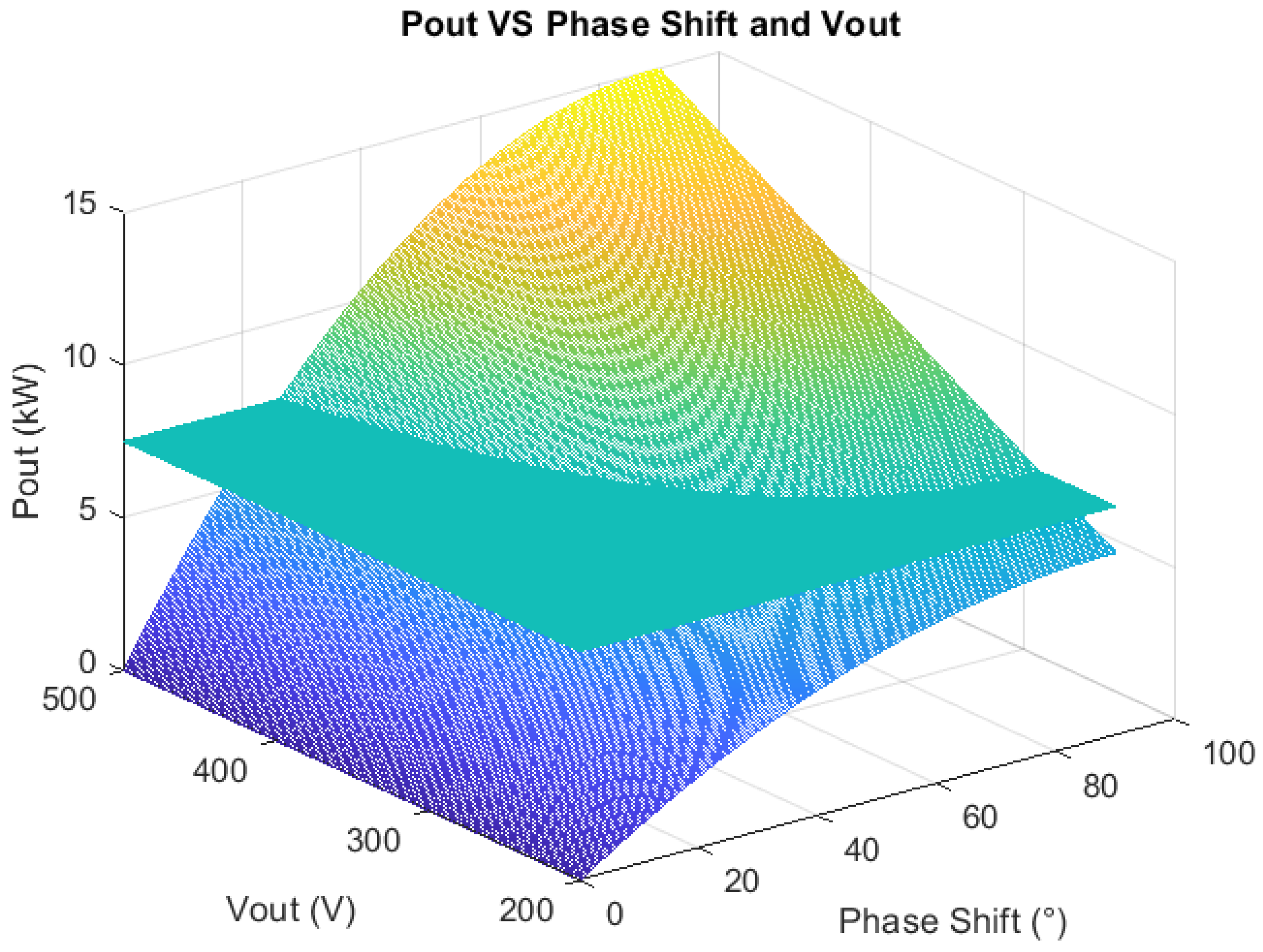
Figure 6, the output power is related to the phase shift and output voltage with a threshold plane at 7.5 kW .
Once these parameters were selected, the converter was modeled and simulated in the PSIM simulation environment. These simulations were also used for the correct selection and sizing of the other components of the converter. Concerning the identification of the DC-link capacitors of both bridges, by allowing a 10 V voltage ripple with the maximum current value flowing in the switches ( 50 A ), the resulting computed capacitance value was 12.5   μ F. Values in the range of tens of microfarads allow the employment of film capacitors, which have a higher voltage rating and less parasitics than electrolytic technology. The DC-link capacitor RMS current, ESR, and ESL must be carefully assessed in DAB converter design because of the high values of circulating currents in SPS modulation, along with unfiltered RMS currents in both the input and output ports. The most stressful operating point is when both the current and power are at their maximum values, and this happens for V o u t = 267 V , where constant current and constant power regions collide. In this condition, the time-domain PSIM simulations showed how the RMS currents on the output and input capacitors are 19.8 A R M S and 28.2 A R M S , respectively. These values set a condition for the maximum ESR of the capacitors. Regarding the ESL, this also must be minimized to avoid high-voltage spikes due to the very fast commutations of the GS66516B switch, with the corresponding d i / d t being as high as 1.3 A / ns . These considerations lead to the use of multiple film capacitors in parallel in order to share the RMS current and obtain a lower equivalent ESL. Three TDK B32776P6226K000 polypropylene film capacitors are used: their main characteristics are C = 22 μ F , V m a x = 630 V , I R M S = 17.5 A R M S ,   and   E S L = 13.2 nH . Even with a wise selection of capacitors, the voltage spikes and ringing on the output voltages are not compatible with the direct connection to a battery in a battery-charging operation. Thus, an additional light LC filter was inserted at the output to remove the voltage spike and ringing and to facilitate an output current control strategy.
A high-frequency (i.e., 200 kHz ) transformer in planar technology was custom made by Himag Planar, Quedgeley, England with a 1:1 turn ratio. In contrast with a wound transformer, the planar architecture provides easier thermal management, the low profile perfectly suits the typical charger form factors, and its realization increases the reliability and the precise control and repeatability of parasitics as the leakage inductance.
The total selected input series inductance L = 8.35 μ H was obtained as the sum of the transformer leakage inductance and external power inductor in series to the primary. The realized component is depicted in Figure 7: the external inductor was realized in the same enclosure of the transformer, practically doubling the transformer volume. The transformer characteristics are shown in Table 5. The specified RMS current was obtained from the simulations. A transformer with a leakage inductance equal to the target value of L = 8.35 μ H would have minimized the dimensions and maximized efficiency (the estimated inductor power loss is 34 W against the 27.6 W of the transformer for full power operations) but was not possible because, to obtain such leakage inductance, the deterioration of the magnetizing inductance would have been too large. Nonetheless, the transformer + inductor component was still very compact (94 mm × 53 mm × 65 mm), and its predicted efficiency at full power was very high ( 99.2 % ) .

3.2. Simulations of Relevant Working Points and Efficiency Evaluation
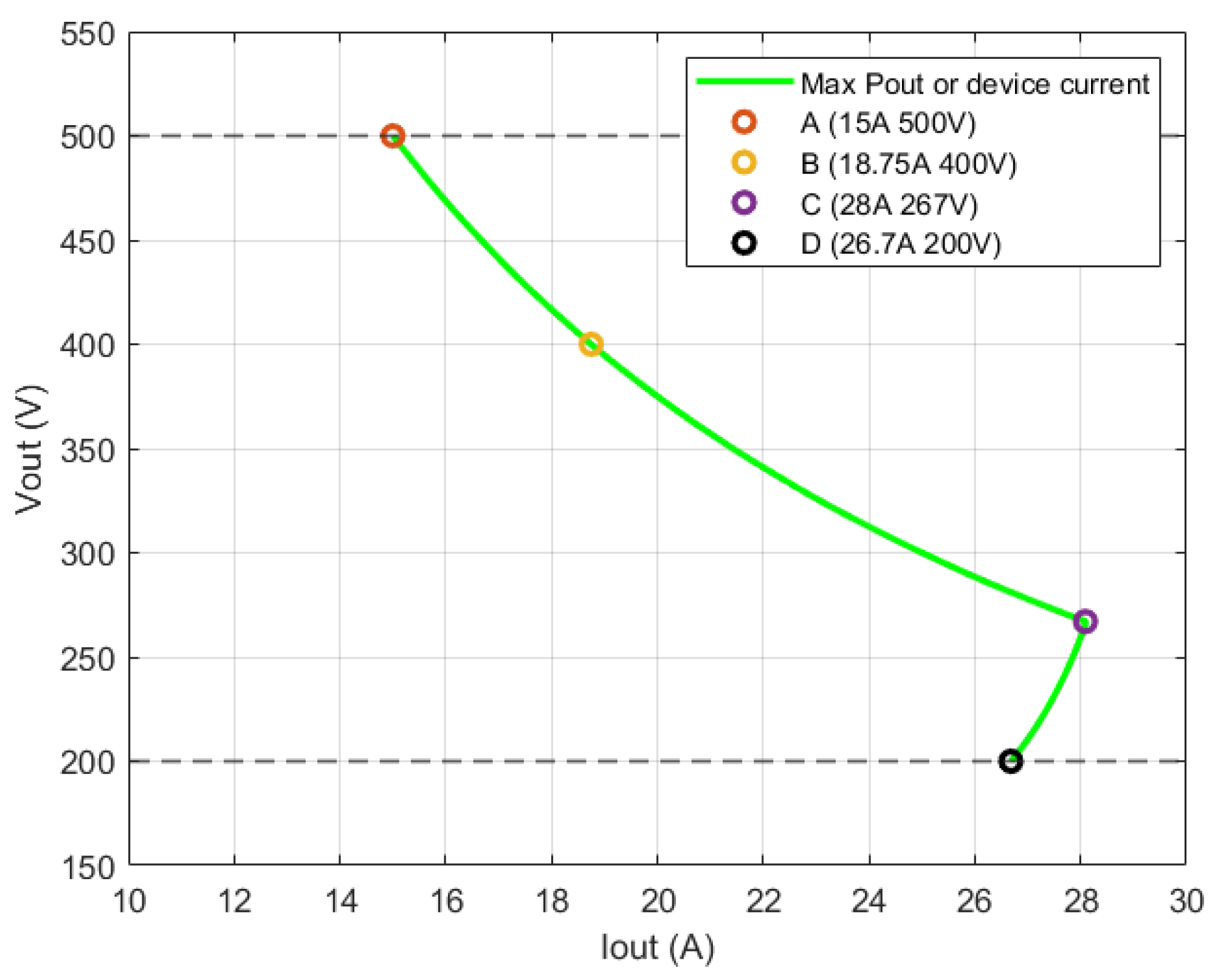
In Figure 8, the computed relationship between the output voltage and output current of the converter is shown. Different relevant operating points are highlighted and were selected for simulations. As discussed before, points A, B, and C are at maximum output power, whereas in D, the output power is limited by the maximum peak current on the switches ( 50 A ). As shown in 
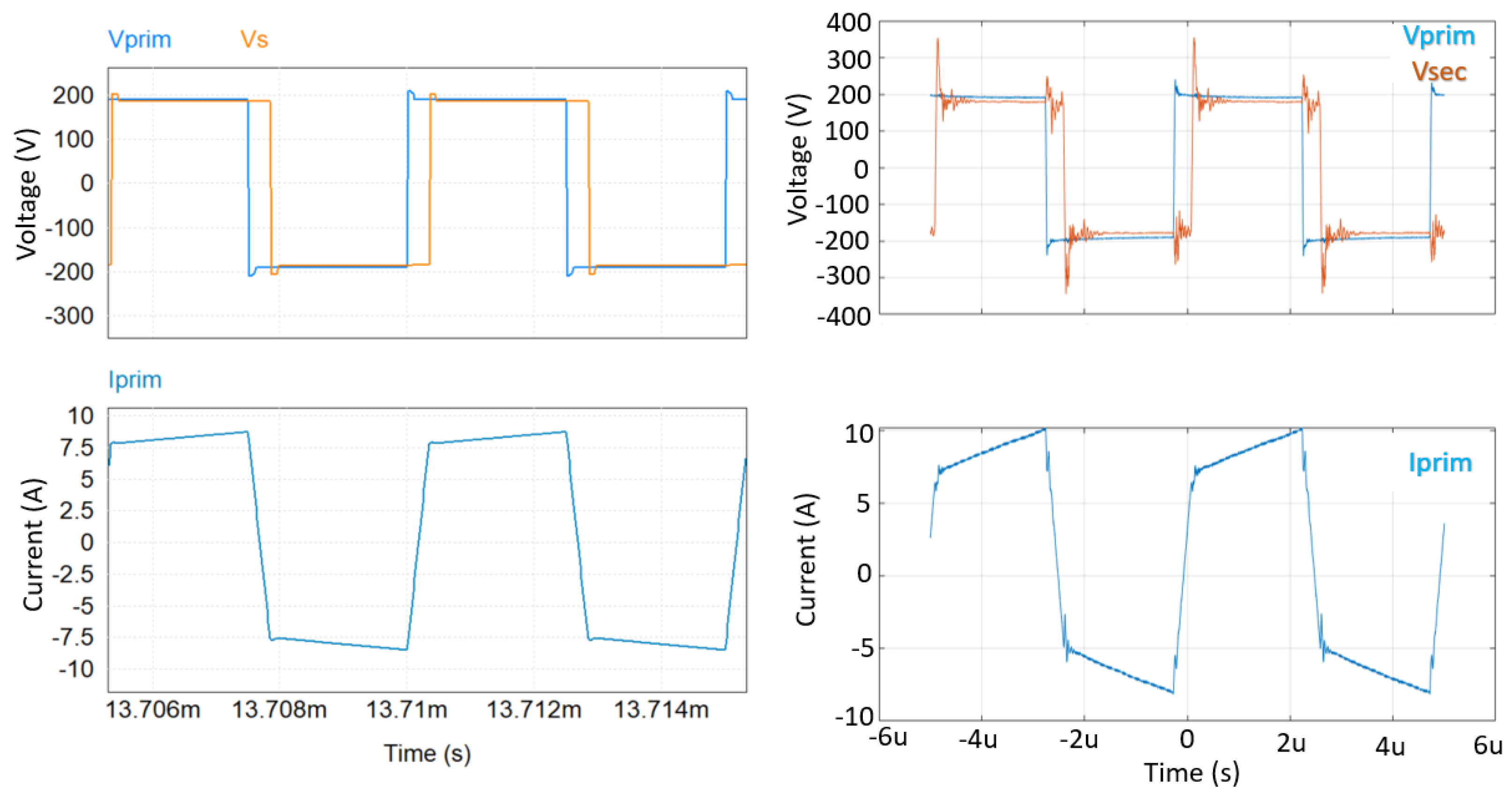
Figure 9, the primary current and the voltages across the primary and secondary windings were obtained through PSIM simulations for each operating point. The different shape of the current allows distinguishing buck mode (points B and C), boost mode (point A), and nominal (i.e., V p r i m = V s e c , point B) conditions. The main results are summarized in Table 6: as expected, the RMS and the peak device current values were the highest in the point C case. Clearly, point B is the most convenient point in terms of RMS currents, controllability, and efficiency; on the other hand, point C is the most stressful operating condition for the converter due to the high circulating currents.
The thermal/efficiency assessment of the converter in the steady-state condition was also computed in PSIM simulations, because the switches were modeled by using “thermal modules” models. These models allowed us to evaluate both the conduction and switching losses of the switches, exploiting a look-up-table approach, thus avoiding long waveform integration during switching events as in Spice-like simulators. Conduction losses were calculated using the I D S vs. V D S characteristics, referred to as the first and third quadrants at different temperatures ( P d i s s , c o n d = V D S I D S during switch conduction). Switching losses were retrieved by inserting E o n , E o f f values for different I D S and V D S switching conditions and the adopted gate resistance ( P d i s s , s w = ( E o n + E o f f ) f s w ). The junction temperature of the switches was computed because the models also accounted for temperature increases due to power dissipation and the thermal impedance of the switch in the actual set up (i.e., also taking into account the isolation layer beneath the devices, the heat sink of the IMS board for each leg, and the forced air velocity of 3 m / s of the cooling system, as described in the next section).
In Table 7, the computed power dissipation values of all the eight GaN devices (four in the primary-side bridge and four in the secondary-side bridge) and their maximum junction temperatures are listed with the losses of the main passive components within the power stage (capacitors, inductance, and transformer, considering all their known parasitics). The ambient temperature used in the simulations was 40 C .
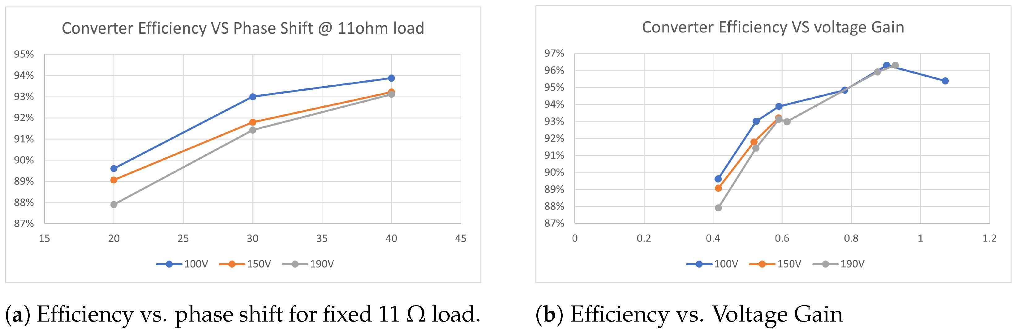
The efficiencies reported in Table 7 are in line with the state-of-the-art efficiencies of DAB converters in GaN technology for charging applications reported in [9,10,11]. The main difference is that the proposed converter delivers twice the power with respect to the one described in [9,10,11]. The converter efficiency is is very high in the conditions close to the nominal one. Indeed, as expected, point B is the most efficient condition for the DAB converter due to the unit voltage gain, where the RMS current is minimized under the same power conditions. The maximum junction temperature reached in the worst condition (point C) is 116 C , which guarantees a large safety margin from the maximum rating of 150 C . The converter is designed to operate at full power at up to a 65 C ambient temperature. Particularly interesting is point D, where the switching losses in the secondary-side bridge are notably low. As described in 
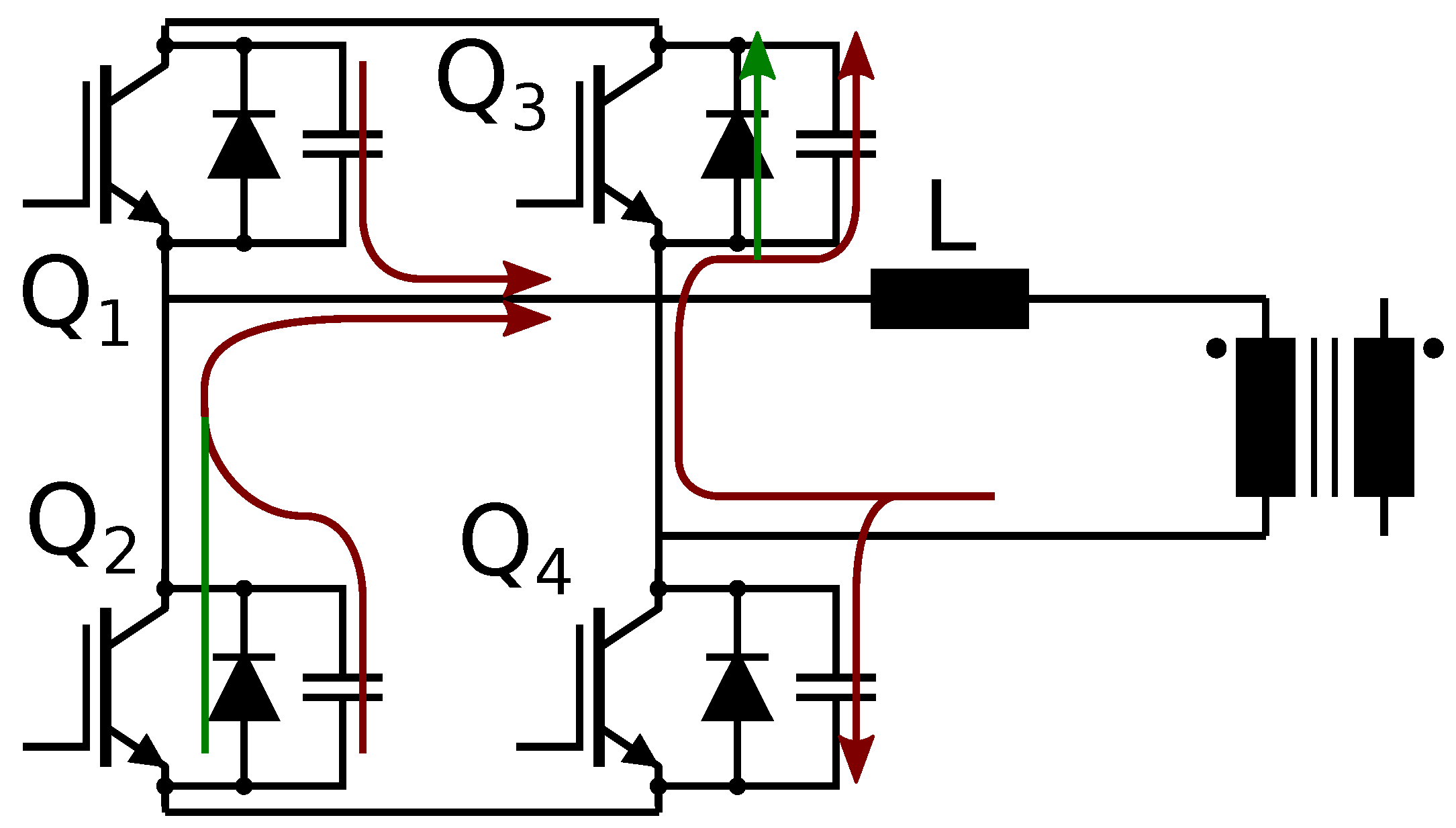
Figure 10, this is due to an almost ZCS behavior, because the drain current of switches Q5/Q8 is near to zero during the ON and OFF transition, whereas Q1/Q4 manage a higher current level at commutations.
Finally, Figure 11 shows how the losses are distributed on the overall system for point B. For these computations, the losses of device drivers and low voltage controlling and sensing circuitry that are described in the next section were considered in terms of budget. It is evident that transistor losses account for more than 70 % of total losses, where 2 / 3 is due to conduction losses, while the leakage inductor overcomes the transformer losses. If the inductance value can be directly embedded into the planar transformer, the efficiency gain would be significant. This graph also points out that the selection of a 200 kHz switching frequency is a good compromise between compactness and performance for this voltage and current levels: at lower current/voltage levels, this GaN technology can switch up to 500 kHz , but for the I/V levels of this circuit, the switching losses at such high frequency would significantly decrease the efficiency. Moreover, the core losses in the transformer would significantly increase at higher frequencies.
From the losses breakdown shown in Figure 11, it is evident that the ZVS condition is very important for converter efficiency maximization. Indeed, the elimination of the turn ON switching losses assured by ZVS makes the switching loss contribution about 1 / 2 of that of the conduction loss, even though the switching frequency is high. For an accurate evaluation of the actual ZVS commutations implemented by the selected components, the Spice model of the GaN transistor and a behavioral model of the drivers were employed to perform accurate time-domain nonlinear dynamic simulations in the Advanced Design System (ADS) simulation environment, which is a circuital simulation tool by Keysight Technologies. 
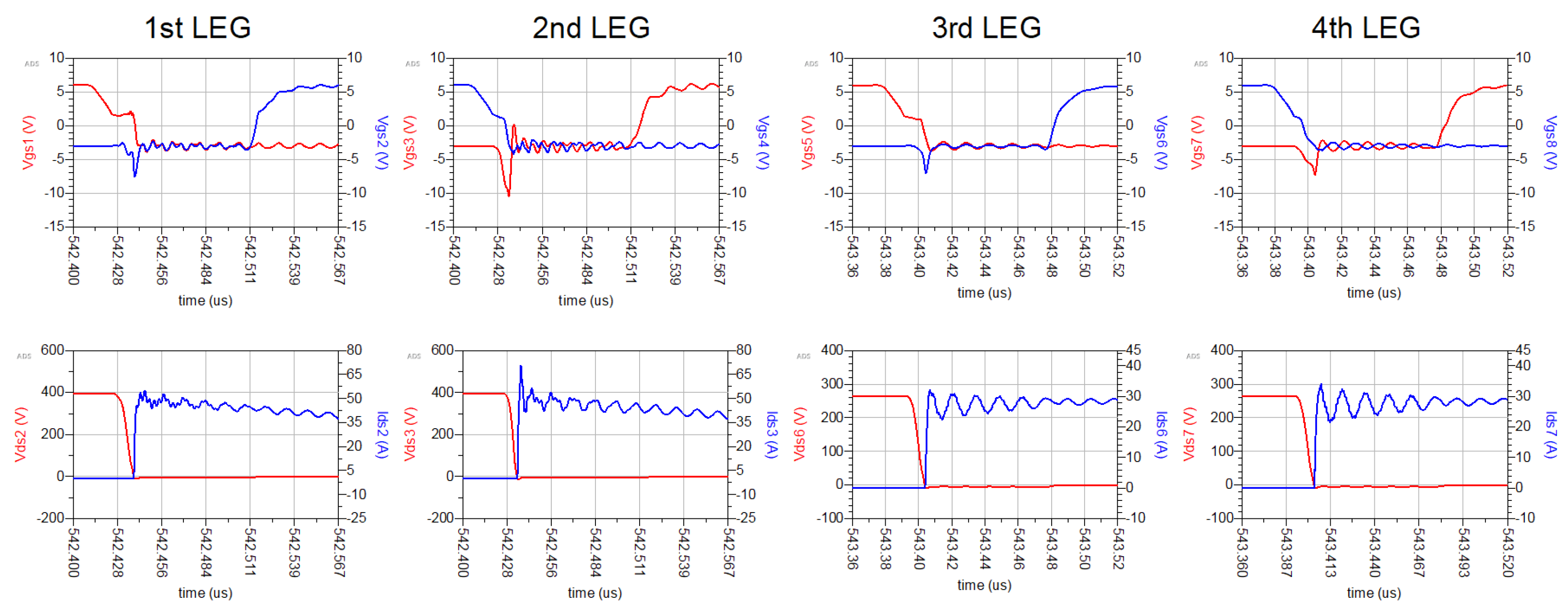
Figure 12 shows the voltage and channel drain-source current of the the switches (lower charts) and gate signals (upper charts) of each device in the DAB converter, during the turn-ON commutations for operative point C. It can be noted how for every switch of the DAB, at the switching off of the complementary transistor (i.e., during the dead time ( 100 ns )), the V D S drops to zero, allowing a lossless switch-ON commutation of the transistor: V D S and I D S (channel conductive current), and the transistors do not overlap in the lower charts.

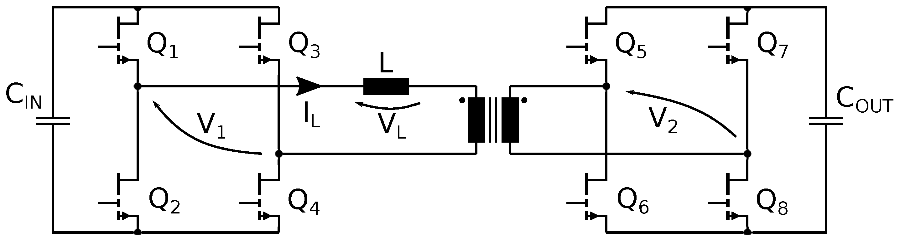
3.3. Architecture of the Prototype Converter

The converter was built following a modular approach and with a sparse component distribution in the main board in order to increase the prototype testability and eventual tweaking. This choice for the first development of the prototype obviously decreased the overall power density, which can be considerably increased in a successive design iteration. The three modules constituting the system were the mother board, control board, and GaN daughter module. The schematic of the entire converter is shown in Figure 13. The mother board was a 265 × 223 mm FR4 PCB with 2 mm thickness with 4 layers of 2 oz of copper to withstand the high current levels of the power section. In addition, a wide exposed copper area, either on top and bottom layers connected by thermal vias, was arranged for the better thermal conductivity of the transformer. The low voltage section was populated by sensors and conditioning circuits of analog signals and by PWM signal traces. Power and low-voltage sections reference grounds were kept separated by a commercial isolated DC/DC AE40-EW-S12 by CUI that acted as an auxiliary supply providing a maximum of 12 V and 3.3 A . This auxiliary supply was largely over-sized for this application and was mainly selected for its availability: the dimensions of this functional block can be widely reduced with a custom design. In the layout design, 1.6 mm and 4.5 mm for clearance and creepage distance, respectively, were applied in conformity with the IEC 61010-1 and IEC 60335-2-29 standards. The control board was a 4-layer 46.2 × 38.1 mm FR4 board specifically designed to implement the control law of the converter. The board received sensed signals from the mother board and output PWM signals. The main component was a UCD3138 [20] controller by Texas Instruments. The controller is a dedicated solution for power supplies characterized by a digital environment that manages a fast hardware state machine. This yielded less general-purpose microcontrollers than the typical C2000 family, with the advantage of being less energy-consuming. In this way, multiple feedback loops could be handled, sectioning fast paths for higher bandwidth response. An important feature is the possibility to generate 4 PWM signal couples at a higher time resolution ( 250 ps ) interlocked by an embedded phase-shift mechanism. The GaN daughter module consisted of two separated boards, a driver board and an IMS board. This solution was implemented to satisfy the need for enhanced thermal management together with minimal parasitics [21]. These boards are described in Figure 14 and Figure 15.
The IMS board was a 45 × 45 mm PCB, where two GS66516B transistors were placed to form a half bridge, while the insulated metal substrate was in charge of conveying the heat produced to the heat sink, minimizing the thermal resistance. The driver board was implemented in a 4-layer 43 × 69 mm FR4 PCB and was populated by isolated gate drivers, isolated DC–DC converters for power supply, and ceramic capacitors for the local DC decoupling of the DC link for the minimization of the power-loop stray inductance. Two isolated single-channel ADUM4121 [22] gate drivers by Analog Devices boosted the digital PWM signals from the microcontroller in two +6/−3 V gate signals with fast transitions and high peak/sink current capabilities, fundamental characteristics when driving WBG devices. Given a maximum skew of the delay time among two different ADUM4121 of 22 ns and the very fast commutation of the switches (delay time + rise/fall time < 40 ns ), a 70 ns nominal dead-time value was selected and implemented in the PWM command generation. The placement of the drivers in the board was optimized to reduce the distance between their output and the gate ports of the transistors as much as possible to minimize the inductance of the gate driving loop. To this aim, a short 2.54 mm connector toward the IMS board was used, and the connection was made with the transistor Kelvin-source.

Sensing

The controller acquired 10 analog signals: 4 currents, 2 voltages, and 4 temperatures, plus a flag signal for over-current protection.
Concerning the first characteristics, the primary current ( I p r i m ), the input current ( I i n ), and two output currents ( I f i l t e r , I o u t ) are sensed. As described in Figure 13, the difference between I o u t 1 and I o u t 2 is the position of the sensor with respect to the capacitance of the output filter in particular. For the current flowing through the primary and leakage inductor, the ACS732KLATR-75AB-T [23] Hall sensor by Allegro was employed. This sensor was able to sense a 75 A bidirectional current with a 1 MHz bandwidth. Its output was opportunely scaled by an OPAMP in differential configuration. The sensor provided a fast flag signal that was set to trigger when the peak current exceeded 65 A. For I i n and I o u t , the MLX91221KDC [24] Hall sensor by Melexis was used. Here, just the DC component was relevant, so high bandwidth was not required. The maximum current sustained was 38 A, which was sufficient to acquire a 28 A I o u t in the worst case ( P o u t = 7.5 kW , V o u t = 267 V ). Regarding I f i l t e r , an ACS724KMA Hall sensor by Allegro was used, which allowed 65 A bidirectional current sensing. Because the current before C o u t had a strong harmonic content, the use of a sensor with wider input range was required. One signal between I f i l t e r and I o u t sensing was provided to the uC by the position of a jumper. The choice could be made depending on the speed of the current feedback loop, because I o u t gives a slower response than I f i l t e r .
All the low-voltage output signals were conditioned by an OPAMP in differential configuration. Voltages at the input and output ports were sensed by two resistive dividers. Because electrical isolation must be kept between the high- and low-voltage sections, the output of divider was provided to an ACPL-C87A [25] Broadcom isolated OPAMP with dual power supply. The V o u t signal was used to close the voltage loop, while V i n was used for OVP and for the feed-forward operation.
The temperature signals provided information about the GaN transistors’ case temperature. A PT100 resistor was placed on each IMS board close to the power devices, giving a good approximation owing to the metal substrate. The variable voltage dropout on the PT100 was managed by a Wheatstone bridge designed on the current rating of the thermistor.

4. Converter Implementation and Experimental Results

In Figure 16, the converter prototype (230 × 348 × 107 mm 3 ) is displayed, highlighting the main hardware sections. As discussed before, the prototype design was not optimized for space saving but for ease of testing and tweaking. In the picture, a large part of the space is occupied by the bulky auxiliary power supply (largely over-sized), the fans (largely over-sized), and the heat sink of the GaN IMS board. All these components could be much smaller in a final implementation of the converter for on-board battery charging applications; in this case, the cooling could probably be liquid, and a more optimized 3D layout could be produced. The compactness of the key components, i.e., the GaN daughter boards, the magnetics, and the DC-link capacitors, is the important aspect in this regard. The functionality of the prototype was tested through the setup schematized in Figure 17a and implemented as shown in Figure 17b. This set up was power-limited, so the converter could not be tested at full power. Further testing will be performed in a future phase. The input voltage was provided by two DC supplies in series connection: an 840 W AIM-TTI CPX400D and a 1.54 kW Delta Elektronika SM 70-22. The maximum input power available was 1.33 kW due to the limitation of the input current ( 7 A ) of the CPX400D. The scope was a MSO-56 Tektronix, the load consisted of power resistors in series-parallel connection, while the master controller was a laptop directly connected to the control board via a PMBus interface forcing a fixed phase-shift value to perform tests in open-loop conditions. Regarding the acquisition of primary current, primary voltage, and secondary voltage, two differential active voltage probes (Aaronia DP1—DC to 40 MHz , and DP25 CHAUVIN ARNOUX—DC to 25 MHz ) and a wide-band DC/AC current probe (Keysight N2783A, 30 A R M S , DC to 100 MHz) were used.
Table 8 illustrates the measured prototype performance for three different conditions in terms of input/output voltages and load resistance. Additionally, in these operating conditions that were largely different from the nominal ones, the measured converter efficiency was remarkably high (even though some percentage points less than what would be expected in nominal conditions). Considering the last operating point in Table 8, in Figure 18, the measured primary/secondary voltages and primary current are in very good accordance with those in the PSIM simulations. This indication of the accuracy of the simulation predictions gave us confidence that the simulated performance in Table 6 and Table 7 at full power was actually delivered by the prototype. In the waveforms in Figure 18, it is noteworthy how the measured secondary voltage displays larger spikes during the transitions than the primary voltage. This was basically due to the effect of the intra-windings’ capacitance of the transformer at the secondary stage, while the effect of the same capacitance at the primary was filtered by the external series inductance. Nevertheless, the effect of such parasitic capacitance does not represent a concern for DAB operation, because the spike amplitude is limited and no time-extended oscillations are present in the high-frequency voltage and current waveforms.
Additional measured data are shown in Figure 19, where the trend in converter efficiency is assessed with varying phase-shift control. Performance improvements seem be linked to higher phase-shift values in Figure 19a; however, this is true only because under the tested conditions, higher phase shift coincided with a voltage gain ( V o u t / V i n ) closer to unity. As described in Figure 5b, unity voltage gain is the best working condition for the DAB.
Finally, it is also interesting to show some pictures provided by the infrared thermal camera that we used during the first prototype assembly and characterization to identify eventual hot spots that may indicate assembly issues or design shortcomings. Figure 20 corresponds to a converter operating in the V i n = 100 V , R o u t = 22 Ω condition, providing insight into the temperature incrases of different parts of the circuit for two different phase-shift control values. The transformer (comprehensive of external inductance) and bulk capacitors remained at ambient temperature, while the GaN modules (mainly their heat sinks are visible) showed a modest temperature variation. Looking at the magnification of the primary side FB in the lower part of the figure, it is possible to appreciate some additional thermal stress in the first leg compared with the second one. From this slight asymmetry in the temperature, it was possible to identify an issue in the layout of the ground loop of this leg in the mother board, which induced a higher stray inductance. This will be fixed in a future iteration of the board to further increase the performance.

5. Conclusions

A 7.5 kW DC–DC DAB converter was designed and implemented, exploiting 650 V GaN technology and planar transformer technology at 200 kHz switching frequency. The converter operates in full power mode from a nominal input voltage of 400 V to a variable output voltage in the range of 267–500 V. For the 400–500 V output voltage range, the efficiency is above 98 % . This efficiency is in line with that of the state-of-the-art DAB converters in GaN technology used for charging applications in [9,10,11], whereas the output power is twice that of the others. The proposed prototype converter is air cooled, and its overall layout has not been optimized for space, but the dimensions of the power bridge modules, magnetics, and DC capacitors show the potential of the selected technologies for very high volumetric power density. This makes this technological solution very attractive for automotive battery charging applications.

Author Contributions

Conceptualization, C.F., A.A., R.M.; methodology, A.A., C.F.; software, A.A.; validation, A.A., C.F.; formal analysis, C.F., A.A.; investigation, A.A., C.F.; resources, C.F, R.M., M.P.; data curation, A.A.; writing—original draft preparation, A.A., C.F.; writing—review and editing, A.A., C.F., R.M.; visualization, A.A.; supervision, C.F., R.M.; project administration, C.F., R.M., M.P.; funding acquisition C.F., R.M., M.P. All authors have read and agreed to the published version of the manuscript.

Funding

This research received no external funding.

Data Availability Statement

The data presented in this study are available in the article.

Conflicts of Interest

The authors declare no conflict of interest.

References

  1. New Registrations of Electric Vehicles in Europe. Available online: https://www.eea.europa.eu/ims/new-registrations-of-electric-vehicles (accessed on 5 March 2023).
  2. Khalid, M.R.; Khan, I.A.; Hameed, S.; Asghar, M.S.J.; Ro, J.S. A Comprehensive Review on Structural Topologies, Power Levels, Energy Storage Systems, and Standards for Electric Vehicle Charging Stations and Their Impacts on Grid. IEEE Access 2021, 9, 128069–128094. [Google Scholar] [CrossRef]
  3. Yuan, J.; Dorn-Gomba, L.; Callegaro, A.D.; Reimers, J.; Emadi, A. A Review of Bidirectional On-Board Chargers for Electric Vehicles. IEEE Access 2021, 9, 51501–51518. [Google Scholar] [CrossRef]
  4. Jung, J.H.; Kim, H.S.; Ryu, M.H.; Baek, J.W. Design Methodology of Bidirectional CLLC Resonant Converter for High-Frequency Isolation of DC Distribution Systems. IEEE Trans. Power Electron. 2013, 28, 1741–1755. [Google Scholar] [CrossRef]
  5. Krismer, F. Modeling and Optimization of Bidirectional Dual Active Bridge DC–DC Converter Topologies. Ph.D. Thesis, ETH Zurich, Zurich, Switzerland, 2011. [Google Scholar]
  6. Dusmez, S.; Cook, A.; Khaligh, A. Comprehensive analysis of high quality power converters for level 3 off-board chargers. In Proceedings of the 2011 IEEE Vehicle Power and Propulsion Conference, Chicago, IL, USA, 6–9 September 2011; pp. 1–10. [Google Scholar] [CrossRef]
  7. Keshmiri, N.; Pradhan, R.; Hassan, M.I.; Emadi, A. An Optimized GaN-Based DAB Converter for More Electric Aircraft. In Proceedings of the IECON 2022—48th Annual Conference of the IEEE Industrial Electronics Society, Brussels, Belgium, 17–2 October 2022; pp. 1–6. [Google Scholar] [CrossRef]
  8. Guan, Q.; Rubino, L.; Wang, Z.; Bozhko, S. Design and Implementation of GaN-based Dual-Active-Bridge DC/DC Converters. In Proceedings of the IECON 2020 The 46th Annual Conference of the IEEE Industrial Electronics Society, Marina Bay Sands Expo and Convention Centre, Singapore, 18–21 October 2020; pp. 2901–2906. [Google Scholar] [CrossRef]
  9. Siebke, K.; Giacomazzo, M.; Mallwitz, R. Design of a Dual Active Bridge Converter for On-Board Vehicle Chargers using GaN and into Transformer Integrated Series Inductance. In Proceedings of the 2020 22nd European Conference on Power Electronics and Applications (EPE’20 ECCE Europe), Virtual, 7–11 September 2020; pp. 1–8. [Google Scholar] [CrossRef]
  10. Schülting, P.; Winter, C.; De Doncker, R.W. Design of a High-Frequency Dual-Active Bridge Converter with GaN Devices for an Output Power of 3.7 kW. In Proceedings of the 2018 International Power Electronics Conference (IPEC-Niigata 2018—ECCE Asia), Niigata, Japan, 20–24 May 2018; pp. 388–395. [Google Scholar] [CrossRef]
  11. Xue, L.; Mu, M.; Boroyevich, D.; Mattavelli, P. The optimal design of GaN-based Dual Active Bridge for bi-directional Plug-IN Hybrid Electric Vehicle (PHEV) charger. In Proceedings of the 2015 IEEE Applied Power Electronics Conference and Exposition (APEC), Charlotte, NC, USA, 15–19 March 2015; pp. 602–608. [Google Scholar] [CrossRef]
  12. POWERSIM Inc. PSIM User’s Manual. 2021. Rev. 1. Available online: https://powersimtech.com/wp-content/uploads/2021/01/PSIM-User-Manual.pdf (accessed on 5 March 2023).
  13. Autodesk. Eagle Manuals. 2019. Available online: http://eagle.autodesk.com/eagle/documentation (accessed on 5 March 2023).
  14. Mi, C.; Bai, H.; Wang, C.; Gargies, S. Operation, design and control of dual H-bridge-based isolated bidirectional DC-DC converter. Power Electron. IET 2009, 1, 507–517. [Google Scholar] [CrossRef] [Green Version]
  15. Giuliani, F. DC-DC Power Converters Featuring Wide-Bandgap Devices. Ph.D. Thesis, Università di Parma, Parma, Italy, 2016. [Google Scholar]
  16. Song, L.; Ramakrishnan, H.; Navaneeth Kumar, N.; Bhardwaj, M. Bi-Directional, Dual Active Bridge Reference Design for Level 3 Electric Vehicle Charging Stations; Technical Report TIDA-010054; Texas Instruments: Dallas, TX, USA, 2019. [Google Scholar]
  17. Chi, S.; Liu, P.; Li, X.; Xu, M.; Li, S. A Novel Dual Phase Shift Modulation for Dual-Active- Bridge Converter. In Proceedings of the 2019 IEEE Energy Conversion Congress and Exposition (ECCE), Baltimore, ML, USA, 29 September–3 October 2019; pp. 1556–1561. [Google Scholar] [CrossRef]
  18. Bottom-Side Cooled 650 V E-Mode GaN Transistor; Rev. 211025; GaN System: Richardson, TX, USA, 2021; Available online: https://gansystems.com/wp-content/uploads/2018/04/GS66504B-DS-Rev-180422.pdf (accessed on 5 March 2023).
  19. Tria, L.A.R.; Zhang, D.; Fletcher, J.E. High-Frequency Planar Transformer Parameter Estimation. IEEE Trans. Magn. 2015, 51, 1–4. [Google Scholar] [CrossRef]
  20. UCD3138 Datasheet; Texas Instruments: Dallas, TX, USA, 2021.
  21. High Power IMS Evaluation Platform; GaN Systems: Richardson, TX, USA, 2021.
  22. ADuM4121/ADuM4121-1 Datasheet; Analog Devices: Wilmington, MA, USA, 2016.
  23. ACS732 and ACS733 Datasheet; Allegro Microsystems: Manchester, NH, USA, 2021.
  24. MLX91221 Datasheet; Melexis: Ypres, Belgium, 2020.
  25. ACPL-C87 Datasheet; Broadcom: San Jose, CA, USA, 2018.
Figure 1. DAB converter schematic.
Electronics 12 01280 g001
Figure 2. DAB waveforms, from top to bottom: the gate signals of Q1 and Q5, primary and secondary voltages, inductor voltage and current VL, IL.
Electronics 12 01280 g002
Figure 3. DAB ZVS mechanism.
Electronics 12 01280 g003
Figure 4. I m a x vs. phase shift at maximum power for different leakage inductances.
Electronics 12 01280 g004
Figure 5. Design characteristics.
Electronics 12 01280 g005
Figure 6. Output power vs. output voltage and phase shift; green threshold plane at P o u t = 7.5 kW .
Electronics 12 01280 g006
Figure 7. Planar transformer with external power inductor.
Electronics 12 01280 g007
Figure 8. DAB converter Vout vs. Iout chart.
Electronics 12 01280 g008
Figure 9. Primary current and primary/secondary voltages for the four operating points specified in Figure 8.
Electronics 12 01280 g009
Figure 10. Junction temperatures, switching power losses, and drain current of Q1 and Q5, with a 40 C ambient temperature at point D Pout = 5.33 kW.
Electronics 12 01280 g010
Figure 11. Distribution of power losses in the overall system at Pout = 7.5 kW; point B.
Electronics 12 01280 g011
Figure 12. ZVS turn-ON condition is met for every transistor in the worst-case scenario of point C.
Electronics 12 01280 g012
Figure 13. Simplified schematic of the entire converter.
Electronics 12 01280 g013
Figure 14. GaN IMS board and driver board.
Electronics 12 01280 g014
Figure 15. GaN daughter module assembly: driver board + IMS board + heat sink.
Electronics 12 01280 g015
Figure 16. Dual active bridge prototype.
Electronics 12 01280 g016
Figure 17. Measurement setup for prototype functionality test at reduced power.
Electronics 12 01280 g017
Figure 18. Comparison between simulation (left) and measured (right) values of primary/secondary voltages and primary current in the V i n = 190 V and R o u t = 24.6 Ω condition.
Electronics 12 01280 g018
Figure 19. Efficiency results for V i n = 100 V , 150 V , 190 V .
Electronics 12 01280 g019
Figure 20. Thermal images of the prototype during V i n = 100 V , R o u t = 22 Ω working operation.
Electronics 12 01280 g020
Table 1. Proposed DC/DC converter specifications.
VinIout MaxSwitching Freq.PoutVout NomVout Min/Max
400 V18 A200 kHz7.5 kW400 V200 V/500 V
Table 2. Commercial WBG power devices potentially suitable for the design.
ProductManufacturerTechnology V DS I DS @ 100 C
IMW65R027M1HInfineonSiC650 V39 A
IMZA65R027M1HInfineonSiC650 V41 A
GS66516BGaN SystemGaN HEMT650 V47 A
R D S C o s s Q r C i s s
27 m Ω 244 pF 239 nC 2131 pF
25 m Ω 130 pF 0 nC 520 pF
Table 3. ϕ and I m a x values for L = 5.3 μ H and P o u t = 7.5 kW .
VoutLPhase ShiftImax
200 V5.3 μ H48.8 73.2 A
400 V5.3 μ H20 21.1 A
500 V5.3 μ H15.6 40.1 A
Table 4. ϕ and I m a x values for L = 8.35 μ H at P o u t = 7.5 kW .
VoutLPhase ShiftImax
200 V 8.35   μ H A
267 V 8.35   μ H 67 50 A
400 V 8.35   μ H 35 23.3 A
500 V 8.35   μ H 26 . 4 32.5 A
Table 5. Planar transformer specifications.
PoutFreqMagn. Ind.Total Input Ind.Turn RatioIn/Out CurrentIn/Out VoltageDimensions
7.5 kW 200 kHz 1.17 mH 8.5   μ H 8 : 8 36 A R M S 200 V 500 V 94 × 53 × 65 mm
Table 6. Main simulation results for the operating points specified in Figure 8.
PointPhase ShiftVoutIoutPout I L , max I RMS
A 24 . 6 500 V 15 A 7.5 kW 33 A 20.9 A
B 35 400 V 18.75 A 7.5 kW 24 A 21.9 A
C 67 267 V 28 A 7.5 kW 50 A 34.4 A
D 60 200 V 26.7 A 5.33 kW 50 A 30.4 A
Table 7. Main results of thermal simulations for the operating points specified in Figure 8. The power dissipations in columns one and two are comprehensive of the four switches of the input and output full bridge (FBs), respectively.
Point P diss , cond / P diss , sw Input FB P diss , cond / P diss , sw Output FB T j Device prim/s P loss Transformer P loss Inductor P loss CapacitorEfficiency
A 31.12 / 30.4 W 46.4 / 38 W 64 / 73 C 12.04 W 28.74 kW 0.44 W 98.1 %
B 39.6 / 22.4 W 42/ 21.6 W 64 / 65 C 12.52 W 29.53 W 0.4 W 98.2 %
C 139.6 / 56.4 W 124.8 / 17.32 W 116 / 95 C 20.24 W 42.17 W 1.9 W 95 %
D 101.2 / 53.6 W 102.8 / 7.20 W 100 / 74 C 17.5 W 37.69 W 1.47 W 94.7 %
Table 8. Measurement results for three different input voltages.
V in Phaseshift I in P in R out V out I out P out eff
100 V 30 3.84 A 384 W 22 Ω 90.2 V 4.1 A 369.8 W 96.3 %
150 V 40 5.03 A 754.5 W 11 Ω 88.4 V 7.96 A 703.6 W 93.2 %
190 V 25 6.43 A 1222 W 24.6 Ω 176.2 V 6.7 A 1176.6 W 96.3 %
Disclaimer/Publisher’s Note: The statements, opinions and data contained in all publications are solely those of the individual author(s) and contributor(s) and not of MDPI and/or the editor(s). MDPI and/or the editor(s) disclaim responsibility for any injury to people or property resulting from any ideas, methods, instructions or products referred to in the content.

