1. Introduction
The communication between neurons is carried out through action potentials (AP), transient changes of a trans-membrane voltage of about 100 mV
PP and few kHz bandwidth. High spatial resolution detection of AP signals (thousands of recording sites/pixels) opens an unthinkable scenario in neuroscience since it allows to observe simultaneously large populations of neurons and their communications [
1,
2,
3,
4]. For several years, the most common technique to observe neurons utilized needle-shaped probes that deeply penetrate the cells, reducing the average-life of the cells to few days due to the irreversible damage caused to the pierced neural membrane but can extract AP signals at high signal-to-noise ratio (SNR [
5,
6,
7]). Recently, state-of-the-art approaches have been widely exploiting minimally-invasive sensing techniques, which are based on CMOS microelectrode arrays (MEAs [
8,
9,
10]). This avoids penetration of the neural membrane and therefore greatly limits tissue damage, allowing months-long observations of neural cultures and opening the road to long-term implants [
1]. However, SNR is heavily reduced due to the lower signal power of extracellular signals.
For this reason, recorded signals are typically improved by advanced post-processing spike sorting algorithms that separate relevant neural spikes (deterministic events) from background noise (random fluctuations), even in presence of very low SNR [
9,
11]. Thus, they deeply analyze the behavior of neurons populations [
11], whereas a complete digital processing hardware implementation is needed to apply event-driven electrical stimulation techniques (e.g., deep brain stimulation) [
12].
Therefore, closed-loop neurons stimulation intrinsically needs advanced electronics systems composed by:
analog stages to acquire the biological signals and perform the conversion into digital domain;
advanced digital spike-sorting algorithms to separate in real-time AP signals from background noise;
electrical stimulation stages that interact with neurons in response to their activity
This work analyzes the digital spike-sorting hardware design. More specifically, a complete action potential detector has been implemented on a Xilinx Spartan 6 FPGA (XC6SLX45-2C, -2 speed grade) [
13] that includes a noise-rejection algorithm based on principal component analysis (PCA [
9]). The hereby proposed neural spike digital detector (NSDD) identifies single AP signals with amplitudes around 200–600 μV that are recorded with a 16 × 192 pixel-submatrix from a 256 × 384 pixel CMOS MEA with an average noise power per pixel of about 100 µV
RMS. It maps in real-time the neural culture electrical activity in terms of total AP number of events (over a time width of 15 s acquisition), AP frequency (enabling the detection of synchronous pattern), and noise power spatial distribution.
Hardware implementation of spike sorting algorithms is very important for implanted devices because of their intrinsic limited power budget. Performing neural activity recognition in situ greatly limits the bandwidth required to transmit data from the MEA and therefore the associated power consumption, at the cost of some additional digital circuitry which however consumes very little power in scaled technologies.
This paper is organized as follows.
Section 2 introduces the experimental setup composed by the neuronal cells culture, the electronics read-out for neural potential sensing/digitalization and the FPGA NSDD.
Section 3 illustrates how the digital spike sorting algorithm has been implemented on FPGA. Finally,
Section 4 provides experimental results in terms of neural network electrical activity mapping, noise spatial distribution and spatial detection of synchronous neural activity. At the end of the paper, conclusions will be drawn.
2. Neural Spike Digital Detector (NSDD)
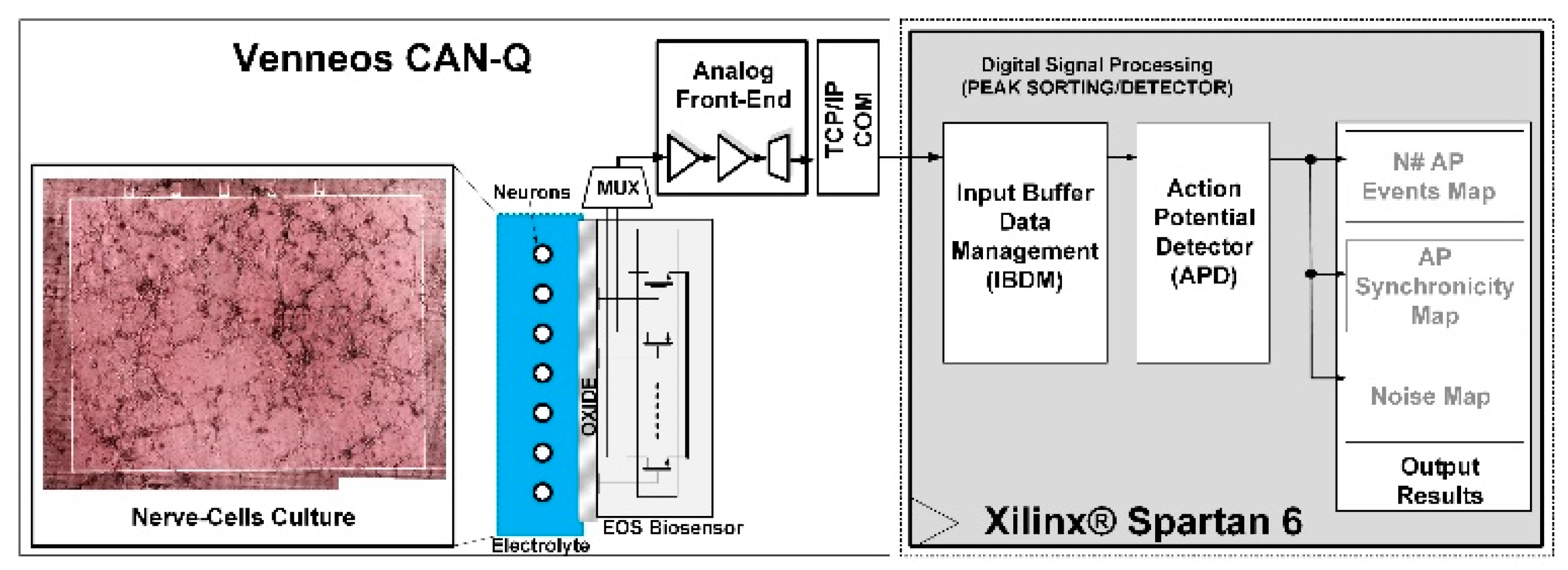
Figure 1 illustrates the top-level block-scheme of the experimental setup described in this work. The neuronal cells dissociated from rat hippocampi are seeded on the CMOS MEA composed by two main stages: the sensor matrix (based on electrolyte-oxide–metal-oxide-semiconductor (EOMOS) transistors) that capacitively senses the neuronal cells electrical activity and the electronics signal processing stages (analog front-end in
Figure 1).
The CMOS MEA is organized in a matrix of 256 × 384 pixels (for an overall 98,304 pixels spatial resolution). The pixels are organized in a hexagonal grid with 6.5 × 5.8 µm pitch. 16 × 192 pixels are time-division-multiplexed to one of 32 analog output channels. The 32 output signals are off-chip digitized.
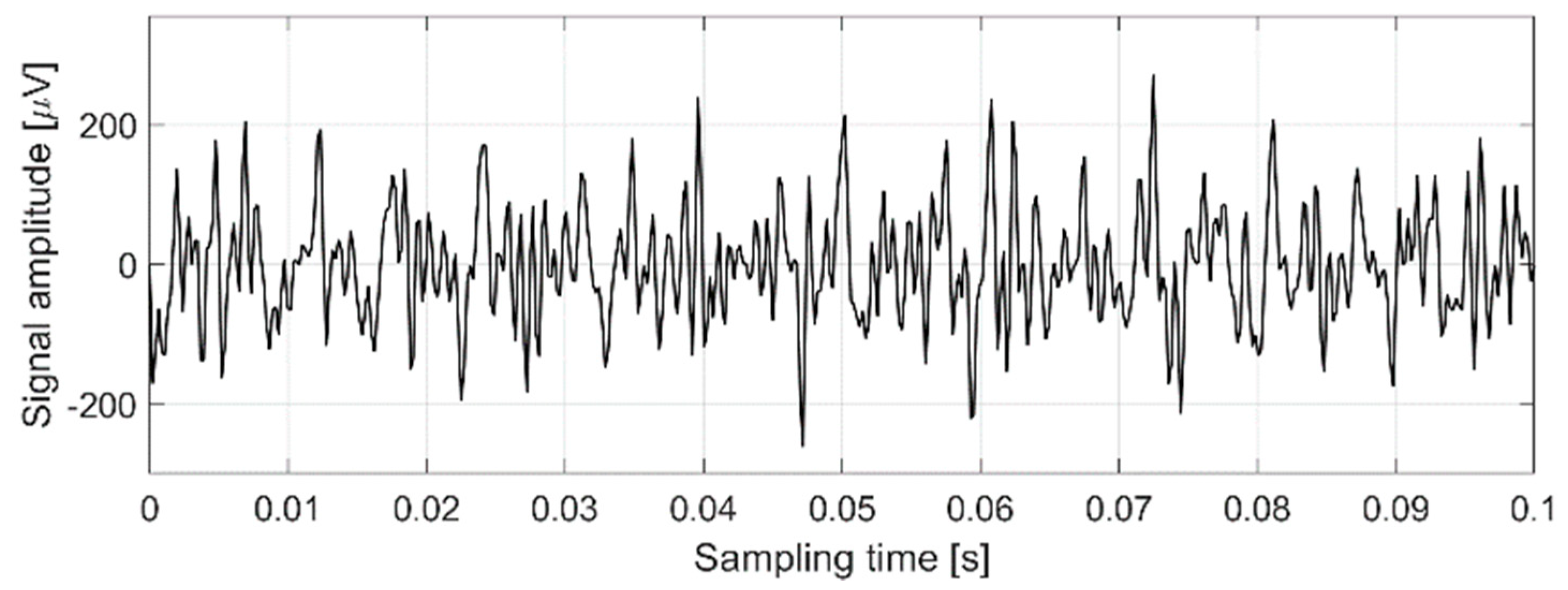
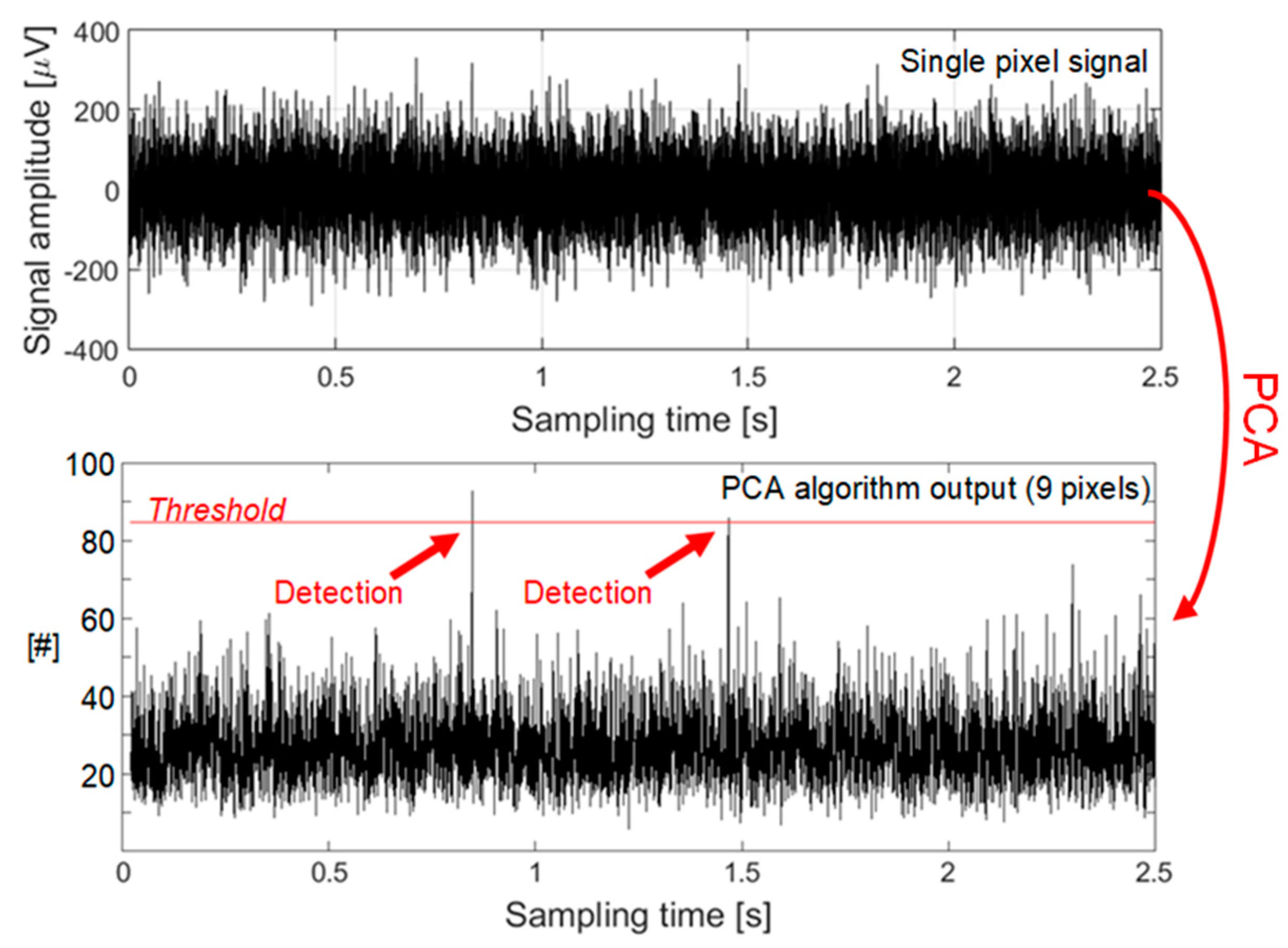
A communication interface (TCP/IP COM) forwards the digitized signals from one selected output to the NSDD FPGA at 14.1 MS/s. The single pixel signal time evolution is shown in
Figure 2 (0.1 s time window and at 4.6 kSample/s).
2.1. Neuronal Cell Culture
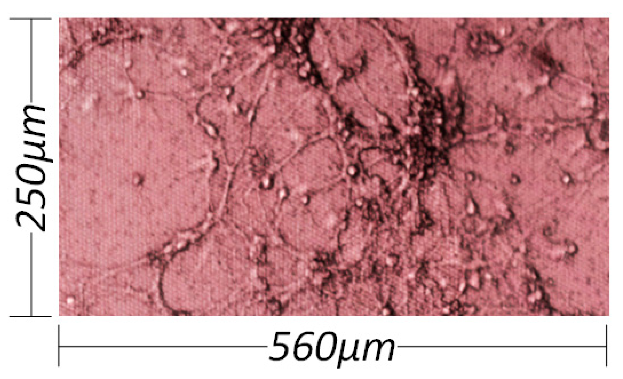
A top-view microscope image of the neuronal cells culture is shown in
Figure 3. After dissociation from the tissue, the hippocampal neurons in culture are able to reconstruct a vital network with specific connections, thus being useful in validating the performance of devices for electrophysiological signal detection.
Wistar rats (Charles River) are maintained in the Animal Research Facility of the Department of Biomedical Sciences—University of Padova. All the procedures involving animals are realized according to Italian and local regulation concerning animal welfare (OPBA Unipd and dL 26/2014). All the reagents and media are from Gibco (Thermo Fisher Scientific - Life Technologies Italia, Monza, Italy). Neuronal cells are dissociated from the hippocampi of E18–E19 embryos, as previously described [
10]. Briefly, the dissected hippocampi are digested in 0.125% Trypsin for 20 min at 37 °C and then dissociated to a single cell suspension in complete DMEM-GlutaMAX-1 (medium supplemented with 10% FBS, 1 u/mL penicillin and 1 μg/mL streptomycin). After centrifugation at 250 g for 10 min, the pellet is gently re-suspended in complete DMEM and pre-plated onto a cell culture dish for 2 h in an incubator at 37 °C and 5% (
v/
v) CO
2 to reduce the percentage of glial cells in the final culture. The collected supernatant is then centrifuged at 250 g for 10 min and the pellet re-suspended in complete DMEM. The surface of the sensors is coated with a proteic layer of poly-L-lysine, that helps neuronal adhesion and differentiation. About 150,000 neurons/cm
2 are seeded on the chip in L15 medium added with 5% FBS and 1% penicillin/streptomycin for 2 h and then maintained in the incubator in complete NeuroBasal medium (added with 2% B27 supplement and 1% GlutaMAX-1). Pyramidal (excitatory) neurons are usually more represented in culture than other type of neurons. The mature neuronal network presents an extensive branching with large amount of synaptic connections [
9]. The experiments are realized on mature cultures at DIV (days in vitro) 20–30.
2.2. Neural Interface Noise
The CMOS MEAs sense the extracellular voltage induced by neurons transmembrane ionic currents. This saves biological tissues from disruptive penetration, does not prevent biological regeneration and finally enable long-time cell observation. Unfortunately, extracellular signal amplitudes are two orders of magnitude smaller compared to more invasive techniques (i.e., intracellular needles probes) and therefore SNR is lower. Moreover, adhesion of cells to the surface increases the noise power [
6]. For this reason, accurate sensing of neural cells electrical activity needs an accurate spatial evaluation of the noise power.
The noise power of the signal has been obtained by analyzing the experimental data coming from a 2.5 s time window of the culture activity, obtaining the noise power spatial map vs. pixels in
Figure 4 (not in scale). It is possible to identify two principal areas, depending on the noise power level: areas without cells exhibit about 80 μV
RMS noise power (blue regions in
Figure 4), while the pixels beneath the cells have higher noise power (120 μV
RMS, yellow/red in
Figure 4).
The difficulty to separate the AP from noise is also evident in
Figure 2 that shows the single pixel time evolution.
Due to the high noise power, using a simple 5∙σ-threshold-crossing detector is not a viable option [
11], because it would lead to discarding most of the action potentials. In particular, with reference to
Figure 2, a 5∙σ-detector at 120 μV
RMS noise would lead to a 600 μV threshold voltage and hence jump over several relevant action potentials events.
2.3. Principal Component Analysis
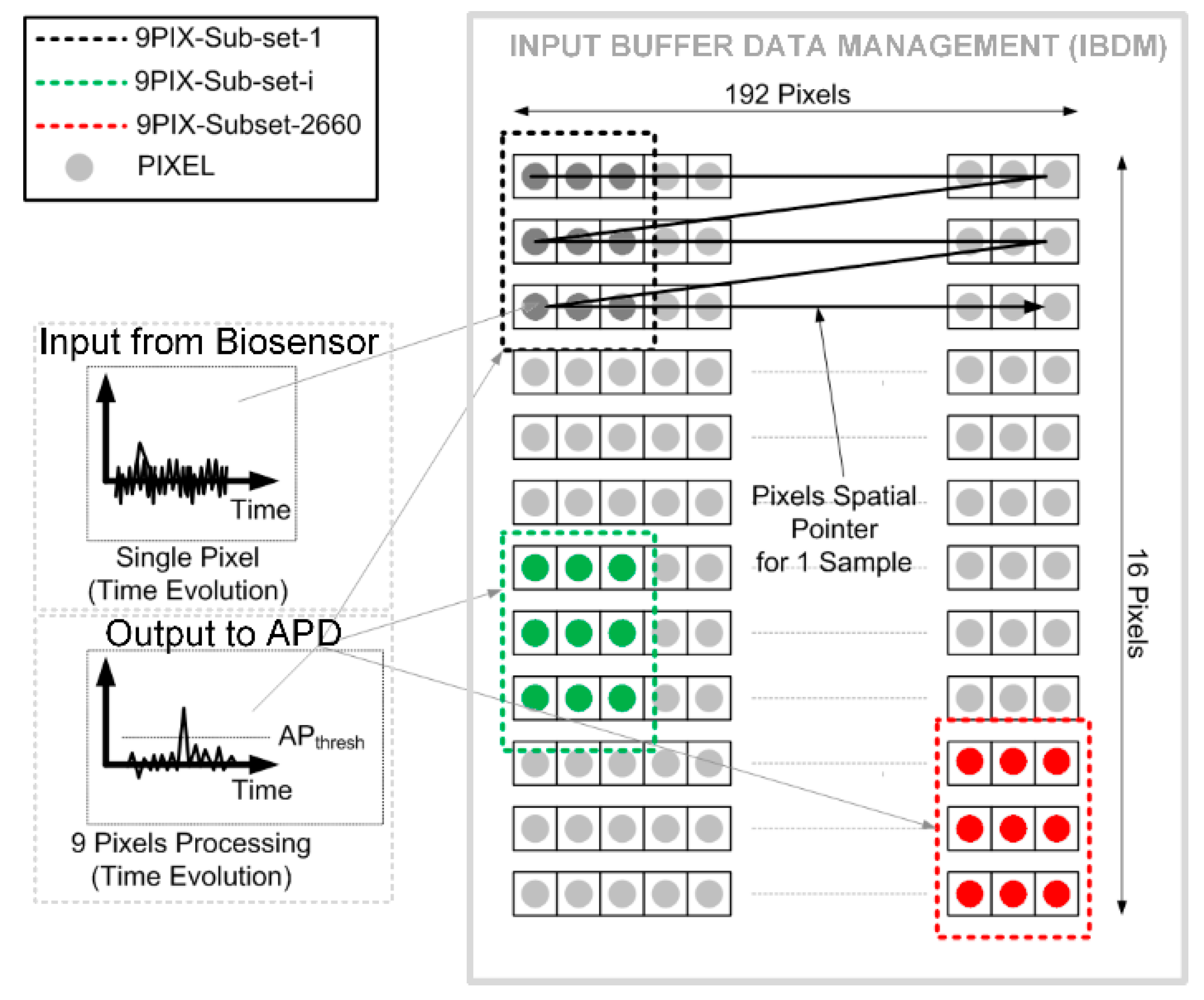
MEAs are characterized by high spatial and temporal resolution that can be exploited by correlation algorithms such as principal component analysis (PCA) [
11]. The pixel density and the sample frequency are sufficiently high that a single AP deterministic event can be detected by nine adjacent pixels for three consecutive time samples (3 × 3 pixel square, see 9PIX-Sub-Set in
Figure 5).
Thus, a single AP can be observed in a total of 27 samples in close spatial/temporal proximity. The PCA algorithm is used to calculate the probability to detect AP events in front of noise (statistical thermal fluctuations).
The AP detection implies to comply with the condition [
9,
11]
where
PIXj indicates the
j-th pixel (sampled at 3 different instants:
n,
n − 1 and
n − 2).
The signal is encoded in a digital word of 14 bits.
σNOISE,j2 is the calculated noise power over the 3 × 3 matrix. Therefore, to separate the eventual AP spike from noise, the algorithm takes nine-pixel sub-set (9PIX-Sub-set as indicated in
Figure 5).
The square sum of three consecutive time-samples of nine adjacent pixels is divided by the noise (i.e., ) and is then compared with the AP detection threshold (AP_Threshold). The AP_Threshold value is calculated imposing that the whole MEA produces one false positive event per second due to noise random fluctuation. Using a MEA subset of 16 × 192 pixels at 4.6 KS/s sampling rate per pixel, the calculated AP_Threshold is 84.6.
Such a technique can improve the global SNR for a sub-set of nine pixels, at the cost of a small spatial resolution reduction (the final spatial map will have 14 × 190 equivalent extracted pixels, since two generic nine-pixel subsets share two columns and are thus partially overlapped).
Figure 6 shows the PCA output for a specific sub-set of nine pixels, compared with the threshold value. After the PCA processing the SNR increases. It goes from 1 dB (without PCA) up to 7 dB (with PCA).
Thus, it is now more reliable to apply a threshold crossing approach (
threshold value is placed at 84.6) and to detect two AP events at 1.9 s and 2.2 s. On average, when no AP occurs, the signal RMS power for each pixel will be equal to σ
NOISE,j. Therefore, on average
will be equal to 1, and the combined 27-samples value
will be 27. The AP detection condition implies that an AP is detected when the PCA output signal (
Figure 6) is higher than 84.6. This leads to a minimum SNR value of at least 7 dB (2).
3. FPGA Neural Spike Digital Detector
The PCA algorithm has been implemented on FPGA by a dedicated digital design that is interfaced with the neurons culture in order to detect and separate APs spikes from noise. The system implementing the PCA is embedded in the NSDD system in
Figure 1 and it also manages the MEA output data rate performing a real time detection of the relevant APs. Thus, it operates by three main stages:
the input-buffer-data-management (IBDM) synchronously receives the data coming from the biosensor via the TCP/IP communication interface;
the action potential detector (APD), that is the digital circuit implementing the PCA algorithm;
a specific set of MATLAB functions that provide graphical representation of the on-going neural activity.
The main requirement for a real time processing of the signal coming from the MEA is that the NSDD data throughput must be equal or higher than the MEA sample rate.
This translates in the Equation (3) condition that correlates the MEA sample rate (
MEAOUT,RATE), the FPGA master clock frequency (
fCLK) and the total number of clock cycles needed to process one sample (
NCLK)
In this way, the APD throughput capability is able to manage the input data rate. This approach has the following advantages:
3.1. Input Buffer Data Management
The NSDD receives a stream of data from the Venneos-CAN-Q machine (VCQ [
14]) via an Ethernet connection using TCP/IP protocol. Data are acquired by the VCQ from the MEA matrix using a specific raster scanning algorithm, whose general procedure is shown in
Figure 5.
Each pixel of the MEA is sampled at 4.6 kS/s and data from the whole pixel matrix are then time-division-multiplexed into a single data-stream that is sent via TCP/IP COM to the input buffer data management stage. The multiplexed data-stream is obtained by transmitting the first time-sample acquired by each pixel, starting from the top-left pixel (first data) and scanning the whole matrix with a raster pattern, thus one-pixel-by-one from left to right and one-line-by-one from top to bottom. After the whole MEA is scanned for the first time-frame, the raster scan is repeated for the subsequent time frames.
The MEA is composed by 3072 pixels and therefore for the first 3072 clock cycles the NSDD receives the first time-sample of each pixel. During the second 3072 clock cycles the NSDD receives the second time-sample of each pixel and then the TCP/IP COM follows this procedure up to the last sample of the last pixel.
The IBDM manages the input data-stream by controlling the Ethernet interface and storing the received data in a dedicated buffer. Then, it sends a data-stream from the buffer to the APD stage to perform the PCA algorithm.
Effectively, Equation (1) establishes that three consecutive time-samples for nine adjacent pixels (27 samples in total) will be used for thresholding. Therefore, the APD can compute the PCA on the first nine-pixel sub-set (corresponding to 9PIX-Sub-set1 in
Figure 5) only after the MEA has been scanned completely two times (3072 + 3072 clock cycles) and the VCQ sends the third time-sample of each pixel of the first two rows (192 + 192 clock cycles) plus the third time-sample of the first three pixels of the third row. Therefore, the first output data comes after an initial start-up time of 447.3 µs (corresponding to a total of 6531 clock periods) that are needed to sense and transfer to the APD all the 27 samples from 9PIX-Sub-set1. After this start-up time, the PCA is performed on one 9PIX-Sub-set per clock cycle, and the 9PIX-Sub-set is moved on the MEA matrix in a raster scan pattern, synchronous to the input data-stream. Thus, after the start-up time latency, the system on FPGA will operate in real-time providing spike detection at the same TCP/IP sample rate (14.1 MHz).
3.2. Action Potential Detector Algorithm
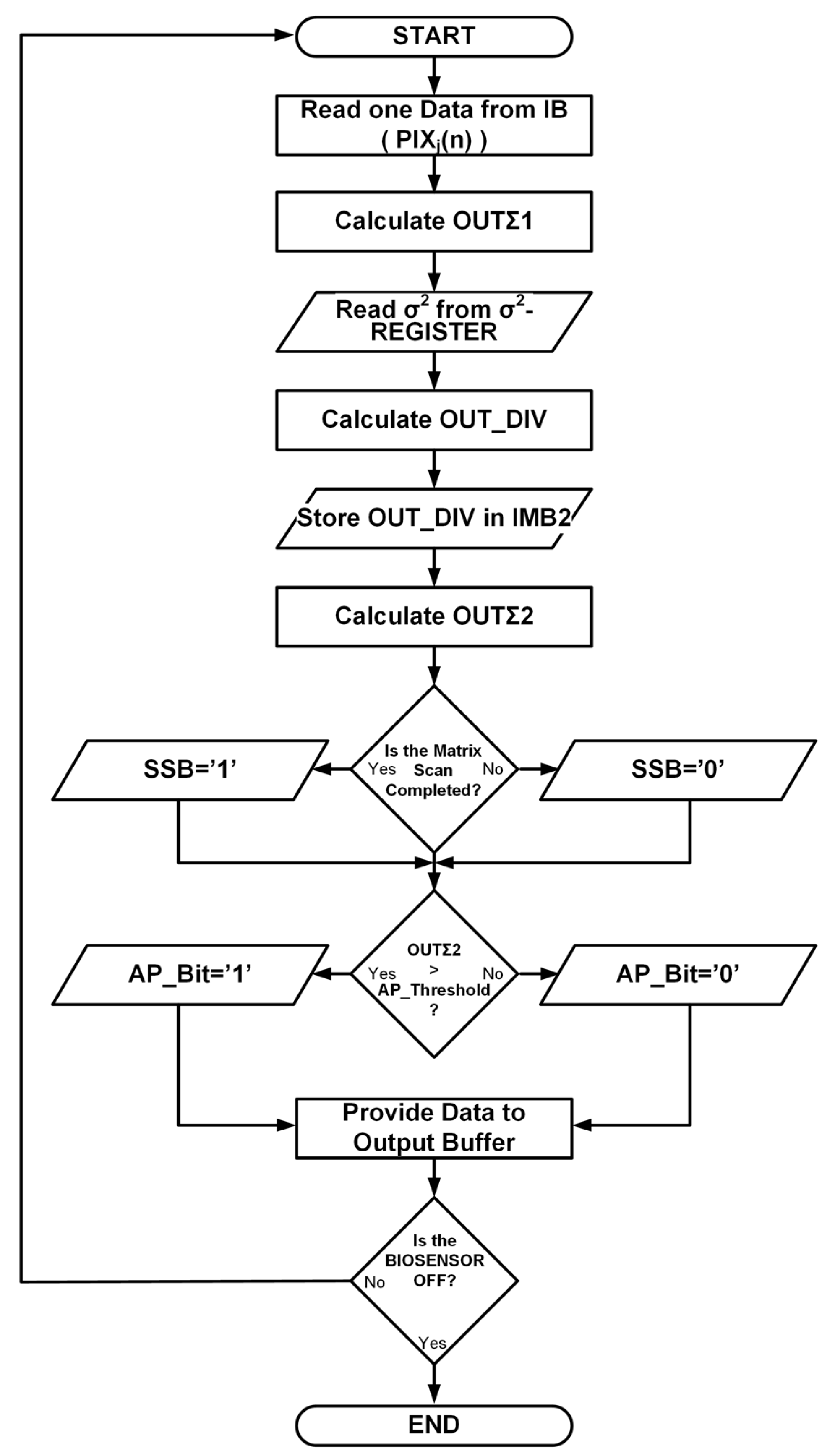
The action potential detector is that stage in the system implementing the PCA algorithm. A flowchart of the FPGA-APD operations is shown in
Figure 7.
Each time a new data (PIXj(n), is received from the MEA, the APD executes the operations illustrated in the flowchart. The algorithm starts reading the input data up to providing an output data. Output data encodes whether an AP has been detected in the n-th timeframe (time pointer) and in the j-th pixel (spatial pointer).
The APD performs all the operations that are required to verify the specific condition expressed in Equation (1). First it calculates the square sum of three consecutive time-samples from the same pixel
PIXj(n), PIXj(n − 1), PIXj(n − 2) are 16-bits data words coming from IBDM. They encode the n-th time-samples of the j-th pixel. Hence j is the pixel spatial pointer (j = 1, …, 3072).
Secondly, it calculates the
OUT_DIV number, which is the result of the division between the
OUT_Σ1 and the RMS noise (
σ2NOISE (
j)) of the
j-th pixel
σ2NOISE (
j) is offline calculated for every pixel, and stored in the
σ2-Register.
The
OUT_DIV data is then stored into an intermediate buffer (IMB) until all
OUT_DIV values of a nine-pixel sub-set are available. Then the sum of
OUT_DIV over nine adjacent pixels is calculated
The
OUT_Σ2 value is compared with
AP_Threshold (stored in a specific 16 bits register) to determine whether an AP has occurred or not
AP_Bit is at ‘1’ logic level if Equation (7) is true, meaning that an action potential has been detected on the 3 × 3 pixel sub-set in the three consecutive timeframes. Otherwise, it is at ‘0’ logic level and no neural activity has been detected.
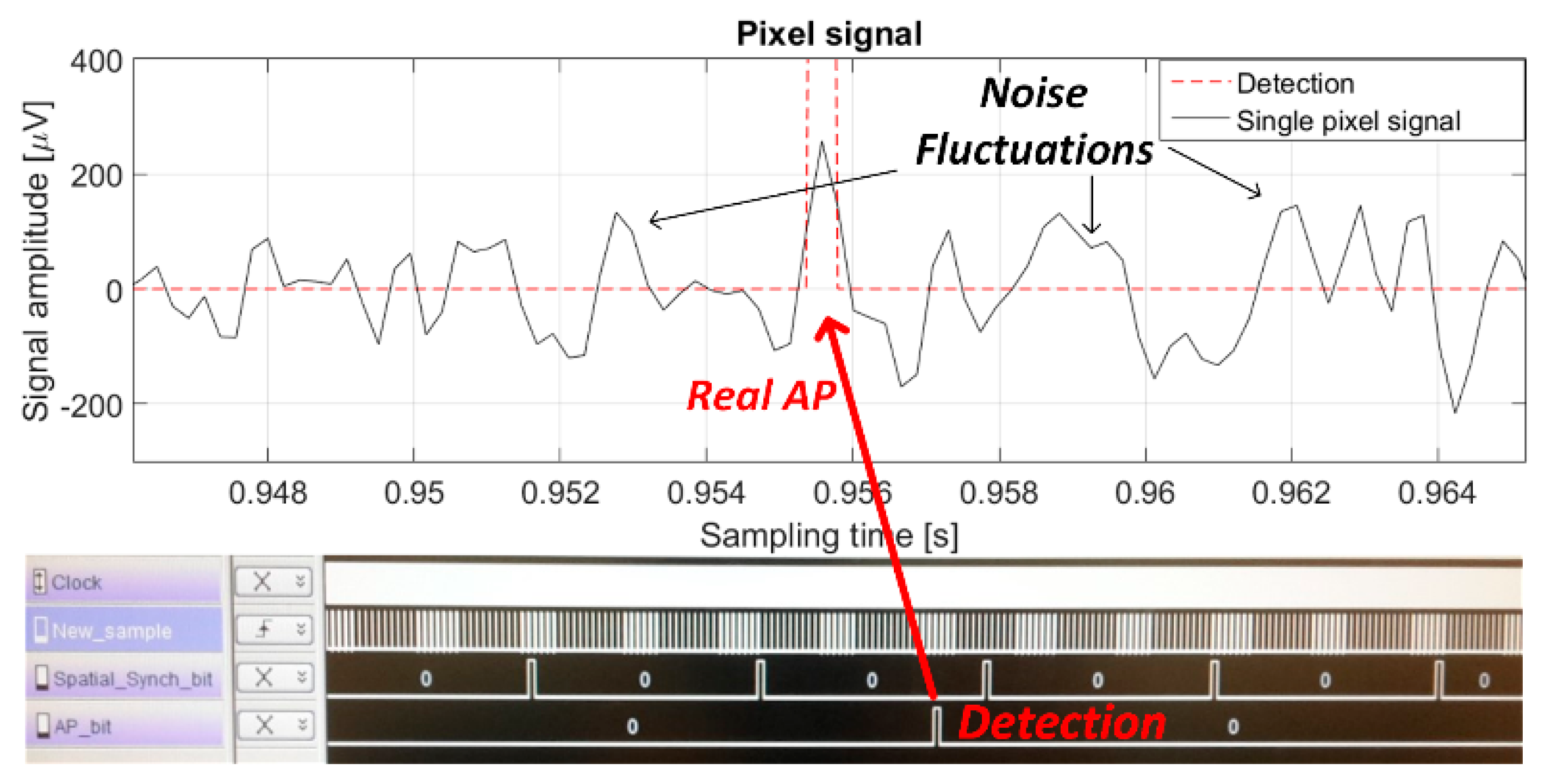
Notice that the algorithm uses a spatial bit/flag (called spatial synchronicity bit (SSB)) whose time evolution w.r.t. the MEA input data stream is qualitatively shown in
Figure 8. The SSB flag is high when the input sample comes from the first pixel of the matrix, otherwise it is low.
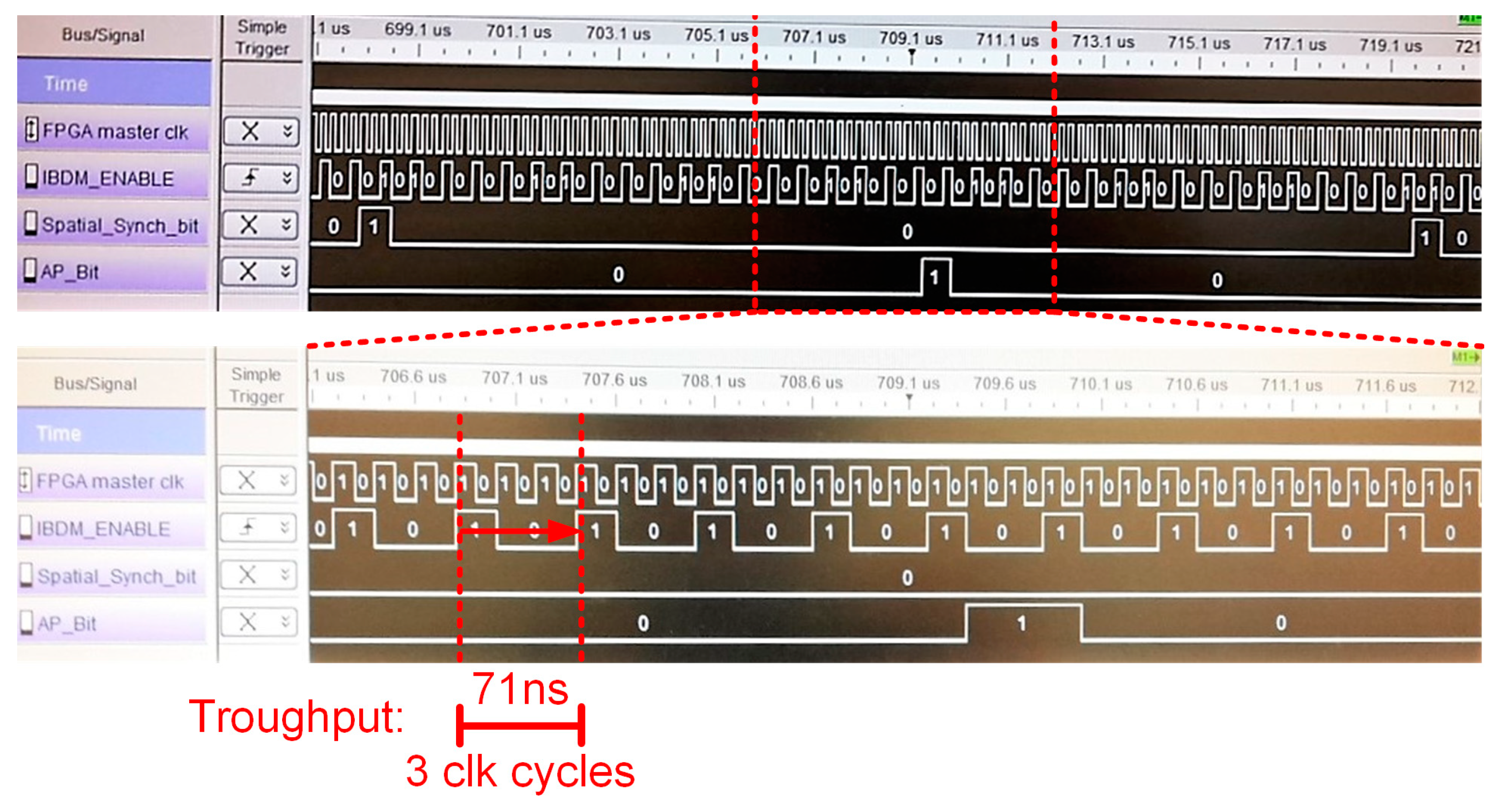
Figure 9 shows the AP_Bit and the SSB time evolution extracted from the FPGA output pins using Agilent 16821A logic analyzer [
15]. The input pattern signals have been directly taken from the experimental setup in
Figure 1.
From top to bottom, the signals recorded by the logic analyzer are:
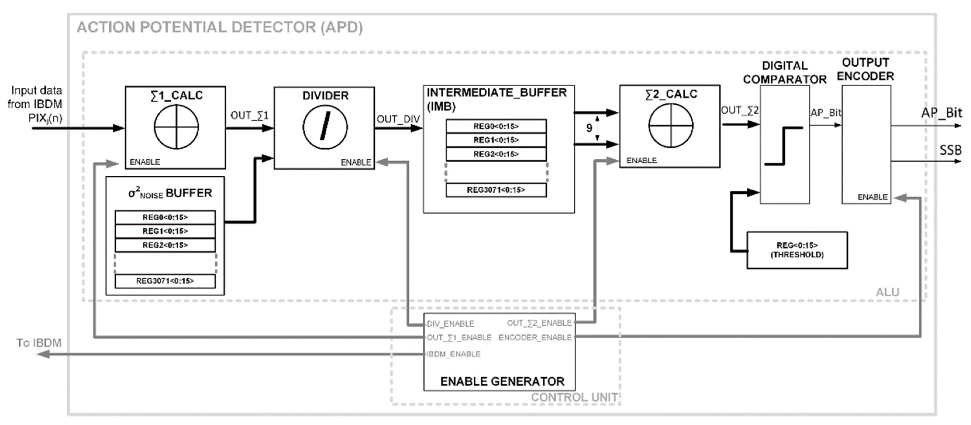
3.3. APD FPGA Hardware Implementation
The algorithm schematized in
Figure 7 has been implemented by a VHDL digital circuit, whose block diagram is shown in
Figure 10. The circuit consists of a control unit (CU) and an arithmetic logic unit (ALU).
The ALU consists of arithmetic, logic, and memory blocks that perform the operations given in Equations (4)–(7). Input data are encoded as signed 14-bit integers, but thanks to their limited dynamic range (cantered around zero and with maximum values around 150–200), can be re-coded with nine-bit resolution (−256 to 255) to limit the hardware requirement without introducing any error. The operations are then performed with unsigned integer arithmetic since after calculating the square value in Σ1_CALC all the values become positive. After each block of the ALU, data are again re-coded to be represented with the minimum resolution compatible with their dynamic range, thus minimizing hardware requirements. The only operation that introduces computational errors while performed with integers is the division, implemented with a Radix-2 algorithm and neglecting the reminder. To minimize this error to below 1%, the numerator (
OUT_ Σ1) has been multiplied by 256 by left-shifting before performing the division. The 256-fold increase in the
OUT_DIV value has then been compensated by increasing the
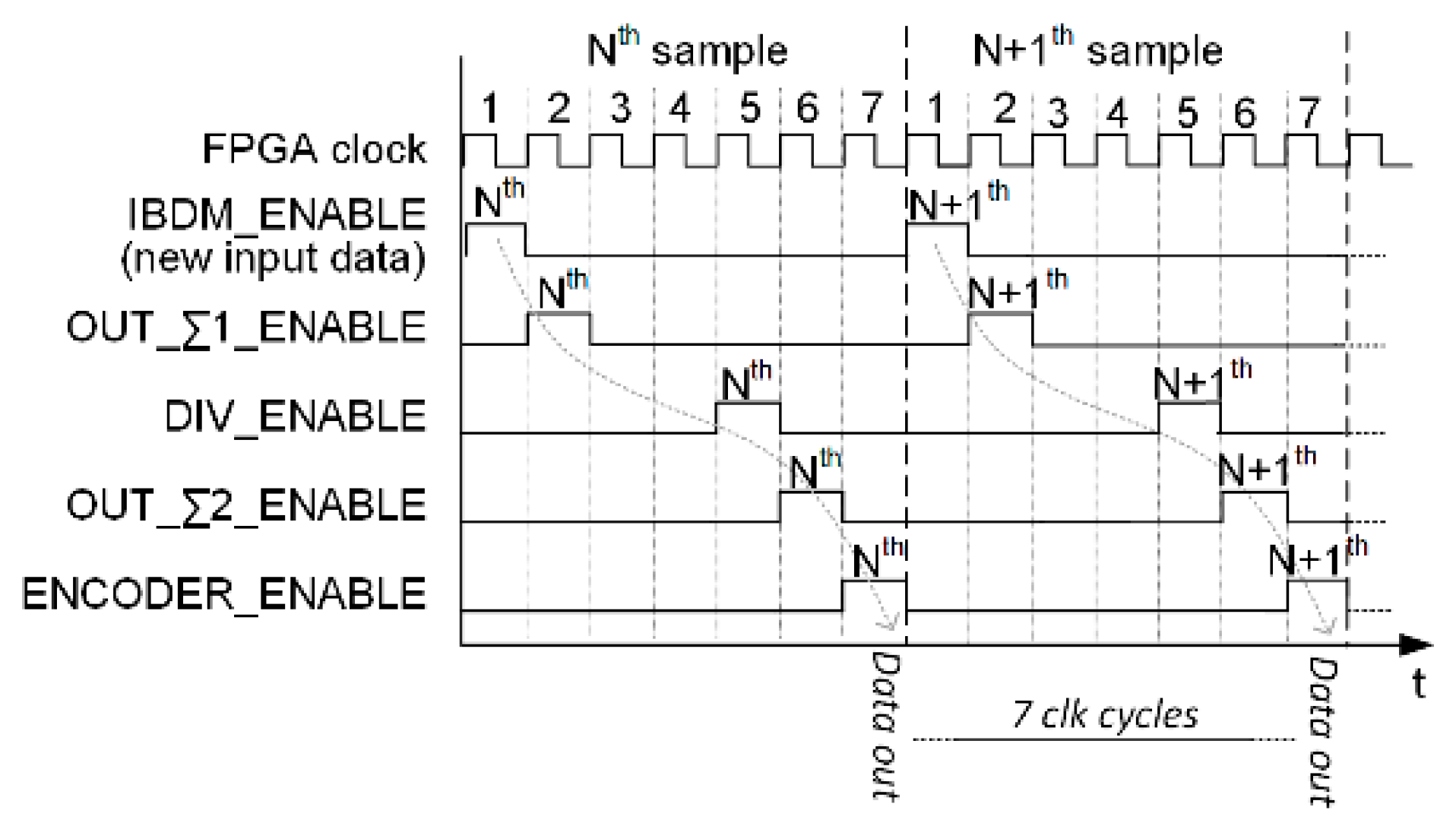
AP_Threshold value by 256 as well. The CU regulates the behavior of the ALU using specific enable signals and spatial pointers. The enable signals sequentially activate the stages of the ALU, controlling the evolution of the algorithm. The time evolution of the CU output signals is illustrated in
Figure 11. When the IBDM_ENABLE signal is high, new data is read from the input buffer in IBDM.
Afterwards the OUT_Σ1_ENABLE, the DIV_ENABLE, and the OUT_Σ2_ENABLE signals are progressively and synchronously activated. The last signal is the ENCODER_ENABLE whose main scope is to regulate the timing of the output signals (AP_Bit and SSB).
Thus, this circuit on FPGA achieves the fundamental objective to encode the entire spatial and temporal activity of the biological neuronal net in three single bits: AP_Bit (that gives the detection information), the FPGA master clock (temporal pointer), and the SSB (spatial pointer).
Each operation is performed during a single cycle of the FPGA master clock, except the division that lasts three clock cycles. Hence, to process a single data, seven clock cycles will be needed in principle. In order to reduce the required clock frequency of the hardware implementation, this design adopts a dedicated pipeline control of the ALU operation as follows. The most relevant FPGA resources utilized for this design are represented in
Table 1.
3.4. APD Control Unit Pipeline Approach
With reference to Equation (3), for a 14.1 MSample/s input data rate, the minimum frequency of the FPGA master clock for a proper control unit operation is 98.7 MHz.
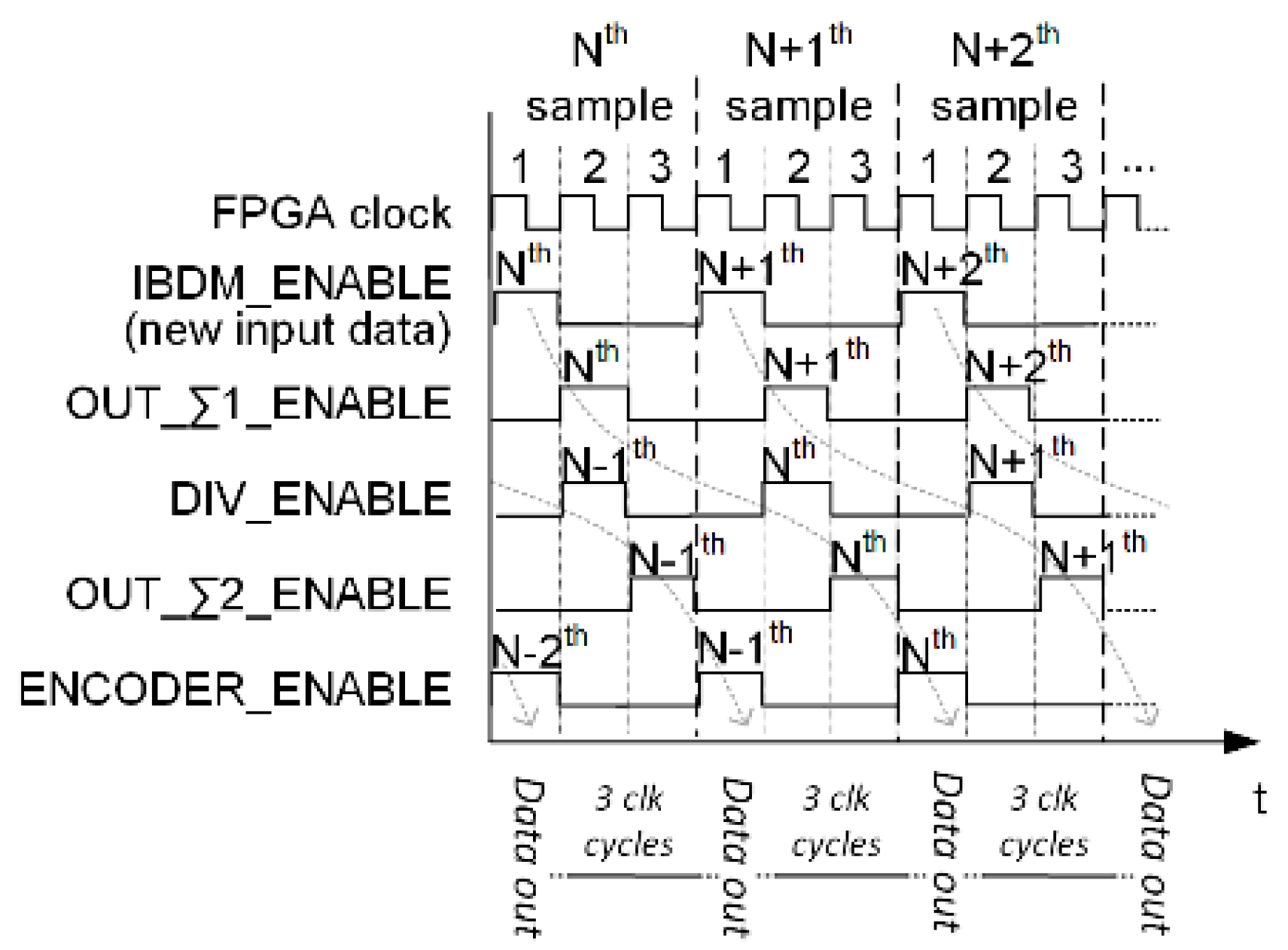
It is possible to achieve the same data throughput with reduced FPGA master clock frequency by using a pipeline approach. The operations in Equations (4)–(7) are scheduled in consecutive clock cycles and the results are stored in separate registers.
Thus, these operations can be executed in parallel, saving time and reducing clock frequency. In fact, when a certain sample (
N-th sample in
Figure 11 and
Figure 12) is processed by a specific stage (Σ1_CALC, DIVIDER, etc.) then such stage waits for six clock cycles for the next data ((
N + 1)-th) without performing an operation and practically entering in stand-by mode.
This intrinsic inefficiency can be mitigated by providing a new data input to the ALU as soon as the first stage (Σ1_CALC) has produced an output.
In this way, the system will accept a new input data every three master clock cycles. Thus, the minimum master clock frequency to handle 14.1 MS/s input data rate will be 42.3 MHz.
Figure 12 shows the CU enable time diagram used in the pipelined APD (P-APD). Each enable is now high once every three clock cycles instead of seven.
Figure 13 shows the output data stream for the pipeline APD. The signal in the second line shows the input data rate, which now requires only three clock cycles to perform all the PCA operations. The final clock frequency adopted in this design is thus 42 MHz.
4. Experimental Results
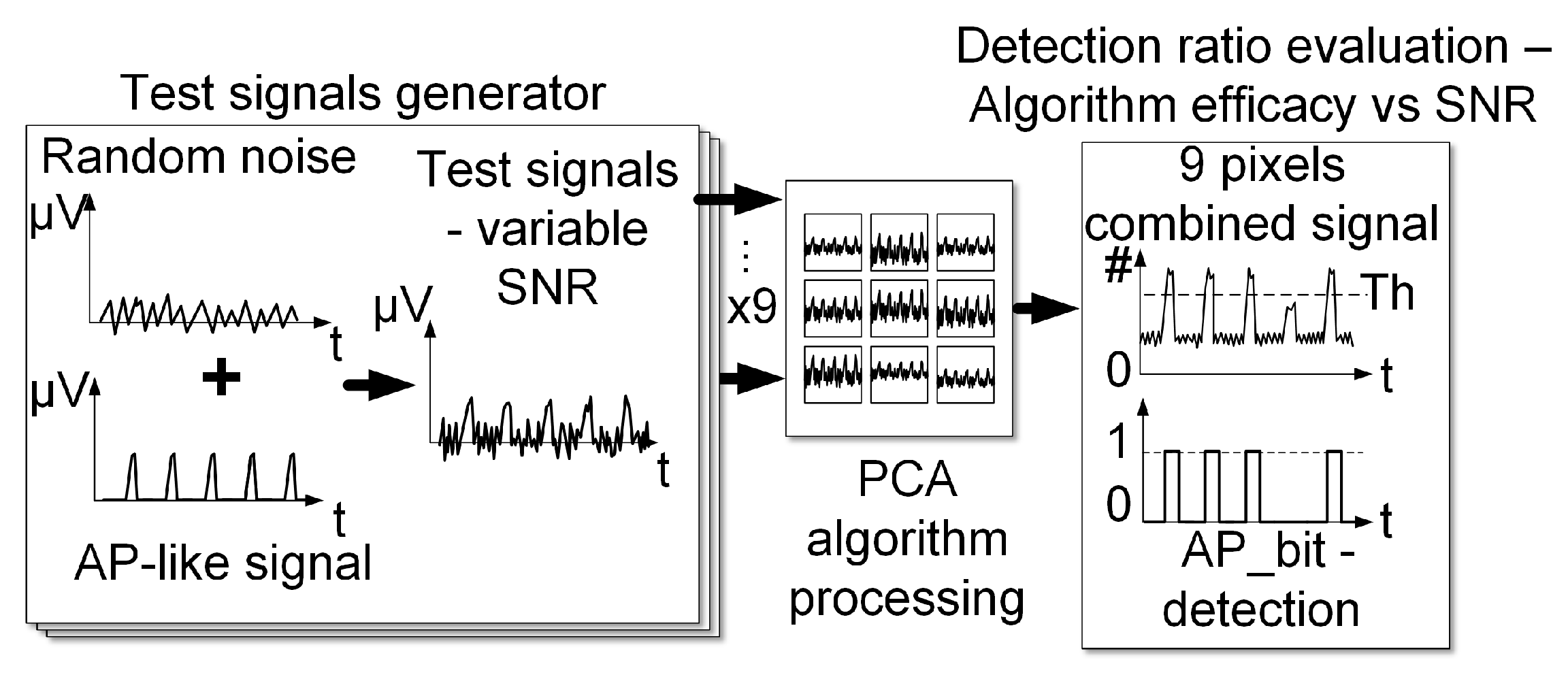
The NSDD for real-time detection of the neural spikes has been validated by two different setups: behavioral and biological. The behavioral setup is a dedicated test-bench schematized in
Figure 14 with the main aim to check the efficacy of the digital system vs. single pixel SNR. It is based on dedicated constructed pattern with a priori known SNR. This test can verify the false positive/negative AP events and quantifying the single pixel SNR range in which the NSDD is able to operate at minimum detection faults.
On the other hand, the biological setup is used in order to directly check the NSDD behavior under the signals coming from the CMOS MEA. This setup has the ultimate scope to detect AP signals under the real-life conditions and manage the effective noise spatial map of the MEA.
4.1. Behavioral Validation
The behavioral validation has been performed at two distinct levels: nine-pixel subset and the whole matrix.
A specific nine-signal pattern has been generated by MATLAB, where each pixel signal has a rate of 4.6 KSample/s and is composed by two main contributions: the noise and 250 AP-like signals spaced of 10 ms with 1 ms time-width.
The duration of each track is 2.5 s. Each spike in the subset has the same phase. The noise power is also the same in each pixel (120 μVRMS) whereas the SNR ranges from 0 dB up to 15 dB (i.e., the last SNR corresponding to a sinusoidal signal at 5∙σ power). This way, since the pattern (and thus the instant in which the AP-like signal will occur) is a priori known, it is then possible to compare the NSDD output bit with the input pattern and to evaluate the robustness of the system (i.e., the eventual fault vs. SNR).
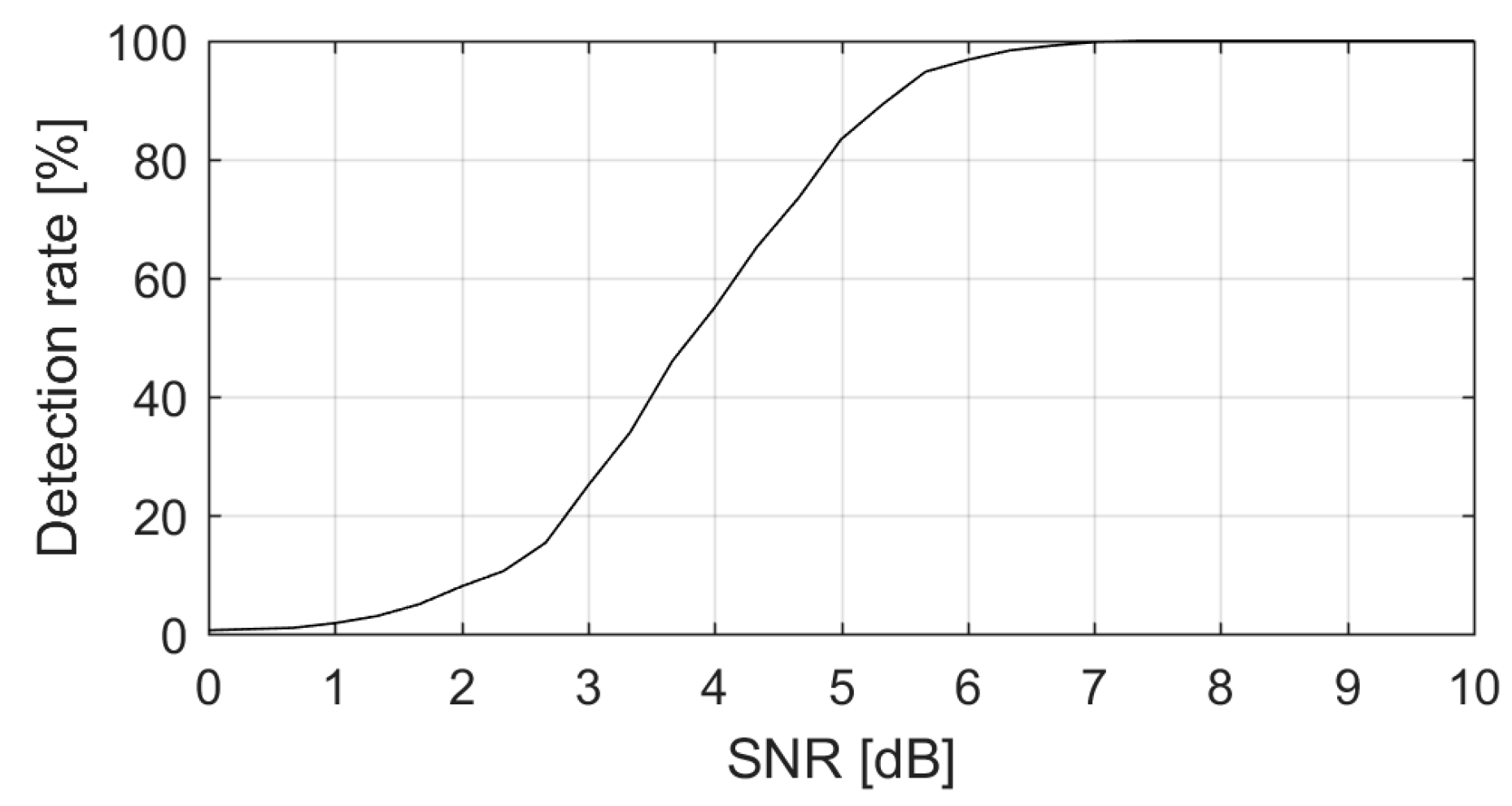
Figure 15 shows the percent value of the detected AP vs. the SNR. Obviously for high SNR (>7 dB) practically all the input APs will be detected by the hardware. At very low SNR the correlation algorithm features a certain detection fault (25% of detected APs at 3 dB SNR), losing several spikes.
Increasing the SNR of the single pixel up to 6 dB the NSDD has very high performance and detects 98% of APs, coherently with the error probability imposed in Equation (1).
APs with 250 μV0-peak amplitude are detected with 98% efficacy.
4.2. NSDD Biological Validation
The NSDD has been finally tested with the signals coming from the neurons culture. The hereby described system outputs in real-time (with 165 ns delay) a binary signal (AP_Bit) encoding spatial and temporal information about the detected neural spikes. This single-bit signal has two important features:
it enables event-driven communication, and/or it can be used for instantaneous control of the electrical stimulation signal;
it can be further processed by dedicated hardware and/or software algorithms in order to perform spatial and temporal mapping of the APs above the MEA.
More specifically, the NSDD system has been tested by monitoring the neurons culture for 15 s and using a dedicated set of MATLAB functions to extract AP information from the real-time generated AP_Bit.
This way, the data coming from FPGA-APD allows representing the neuronal cells culture electrical activity by:
neural spike spatial map, representing the cumulative number of AP vs. pixel for a given 15 s acquisition time;
noise power spatial map, showing the noise power spatial distribution within 2.5 s single pixel time evolution;
action potential bursting map, detecting eventual synchronous spikes activity over the entire MEA covered area (time window is again 2.5 s).
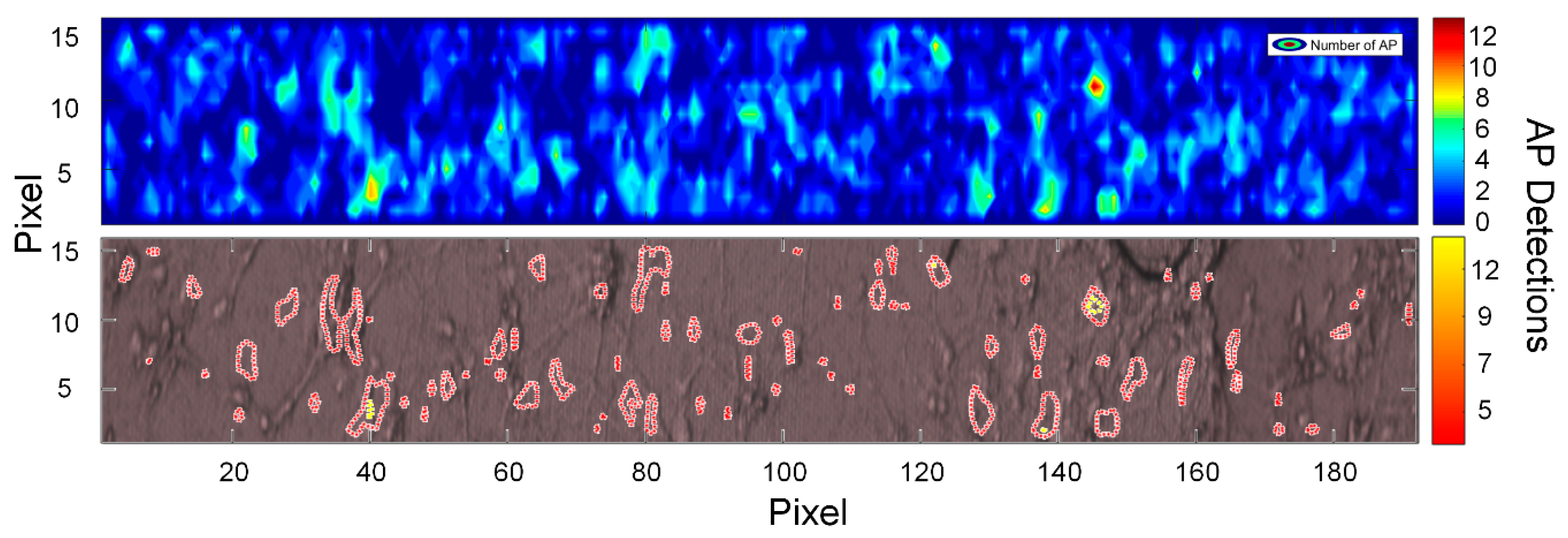
Figure 16 shows the neural spike spatial map where colour intensity is related to the local neuron activity detected by the NSDD in 15 s time window. Notice that yellow/red regions point out 6/12 spikes over 15 s, resulting in the highest AP rate over the given time window. It has been shown that hippocampal neuronal cell cultures exhibit spontaneous electrical activity with rates coherent with the ones observed by the NSDD [
10]. For sake of completeness,
Figure 16 also shows the neural spike map superimposed on the culture photo.
4.3. Action Potential Bursting
The AP_Bit can be used to detect whether any synchronous activity of the neuron population is happening at any given moment. Simultaneous spiking by multiple neurons could hint at particular medical conditions such as the beginning of an epilepsy seizure. In order to produce strong synchronous behaviours in cell cultures, external chemical/electrical stimulations are usually required [
16,
17]. However, for this experiment no external stimulus has been provided, and therefore only minor synchronicity levels have been observed. More precisely, by counting the total APs detected over 10 ms time-windows, few points over MEA area have shown at some point some (casual/random) synchronous spiking.
Figure 17 shows the total number of synchronous spikes referred to the whole MEA during a 10 ms time window. It is possible to observe that some pixels have disclosed some synchronous spiking, for example between 910 ms and 920 ms a total of four areas on the MEA produced some APs. The correspondent spatial map for this particular bursting event is also shown in the bottom part of the same
Figure 17. This demonstrates the capability of the proposed system to operate in complex cultures where a more pervasive synchronous activity is imposed. In fact, the NSDD minimizes the data volume produced by the MEA by efficiently encoding only the relevant information about actual neuron activity. This greatly simplifies the real-time implementation of subsequent higher-level algorithms such as AP bursting detection or, more generally, algorithms that can detect neural patterns and abnormal neural activity (i.e., epileptic seizures).
5. Conclusions
This paper presents the design of a complete FPGA-based digital circuit that monitors the electrical activity of a hippocampal neuronal cells culture over a micro-electrode array and detects action potentials from background noise. The system has been almost entirely implemented by dedicated hardware solutions that allow real-time detection of the on-going neural activity and encodes the temporal and spatial information using a dual bit stream at 14.1 MHz. The system is composed by the VHDL-based FPGA design and a proper set of MATLAB functions for data evaluation. A behavioral validation testbench has been developed and has been used to extrapolate the algorithm detection efficacy vs. SNR.
The system has been experimentally validated by producing a spatial map of the on-going electrical activity, which was shown consistent with spontaneous neural activity rates. The hereby proposed system can also provide the spatial distribution of the noise power over the biosensor, which is linked to adhesion/presence of cells over the MEA surface. Finally, the output bit-stream has been used to detect AP bursting events, highlighting synchronous neural activity over the biosensor.

 ,
, 


