Router-Integrated Cache Hierarchy Design for Highly Parallel Computing in Efficient CMP Systems

1
Graduate School of Information, Production and Systems, WASEDA University, Wakamatsu-ku, Fukuoka 808-0135, Japan
2
Electrical Academy, Jiangxi University of Science and Technology, Ganzhou 3410000, China
*
Author to whom correspondence should be addressed.
Electronics 2019, 8(11), 1363; https://0-doi-org.brum.beds.ac.uk/10.3390/electronics8111363
Submission received: 20 August 2019
/
Revised: 28 October 2019
/
Accepted: 15 November 2019
/
Published: 17 November 2019
(This article belongs to the Special Issue Low-Power Techniques for Embedded Systems and Network-on-Chip Architectures)
Abstract
:In current Chip Multi-Processor (CMP) systems, data sharing existing in cache hierarchy acts as a critical issue which costs plenty of clock cycles for maintaining data coherence. Along with the integrated core number increasing, the only shared cache serves too many processing threads to maintain sharing data efficiently. In this work, an enhanced router network is integrated within the private cache level for fast interconnecting sharing data accesses existing in different threads. All sharing data in private cache level can be classified into seven access types by experimental pattern analysis. Then, both shared accesses and thread-crossed accesses can be rapidly detected and dealt with in the proposed router network. As a result, the access latency of private cache is decreased, and a conventional coherence traffic problem is alleviated. The process in the proposed path is composed of three steps. Firstly, the target accesses can be detected by exploring in the router network. Then, the proposed replacement logic can handle those accesses for maintaining data coherence. Finally, those accesses are delivered in the proposed data deliverer. Thus, the harmful data sharing accesses are solved within the first chip layer in 3D-IC structure. The proposed system is also implemented into a cycle-precise simulation platform, and experimental results illustrate that our model can improve the Instructions Per Cycle (IPC) of on-chip execution by maximum 31.85 percent, while energy consumption can be saved by about 17.61 percent compared to the base system.
1. Introduction
In modern Chip Multi-Processor (CMP) systems, cache hierarchies are too large to support highly-parallel computing as the number of cores stacked in one chip is increasing rapidly. Since those cores and caches crowd into the single-chip area, data flows in many concurrent threads become too complicated to achieve the desired throughput [1]. Thus, the routing network is promising to efficiently solve the interconnection problem, which can transmit vast amounts of data among cores and caches [2]. Furthermore, the recently proposed stacked on-chip architectures can efficiently work by allocating cores and cache hierarchies into different layers, which leads to on-chip components in adjacent layers in 3D by Through Silicon Vias (TSVs) [3], thereby decreasing the physical routing distance and latency.
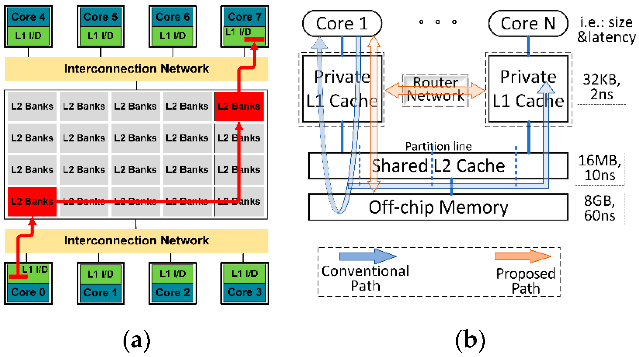
During highly-parallel computing, sharing data in cache hierarchy happen frequently and cause serious data coherence issue, where the sharing data are defined as the target data of the current private cache accesses while those data are already existing in the private caches of other threads. However, conventional CMP architectures (i.e., dance-hall structure) can maintain sharing data with the aid of complex and expensive device operating in the shared cache [4]. For example, as shown in Figure 1a, sharing data in two private caches requires very complex data maintenance operations if any alteration happens to those sharing data. And if an access request from some core encounters an access miss in both its private cache and partitioned bank group [5], but the target data are already existing in other bank groups, complex target data migrating operations are required (i.e., directory-based coherence protocol), thereby consuming plenty of clock cycles. Inspired by data interconnecting among Processing Elements (PEs) in the Network On a Chip (NoC), we are motivated to establish a specialized router network for detecting sharing data and maintaining data coherence. As shown in Figure 1b, if those detected sharing data can be handled in the private L1 cache level, a large proportion of access latency can be saved in the proposed path rather than the slow and expensive conventional path.
In our previous work [6], we proposed a filter router for an efficient stacked shared cache and further designed the router architecture to evaluate its performance and energy consumption in detail. However, limited improvements can be achieved because the amount of harmful shared cache accesses filtered by the previous router is far less than the one of private cache accesses on both emerging frequency and scale, where those harmful accesses in private caches cause much more serious performance degradation. Thus, in this work, we are motivated to propose a router-integrated private cache architecture to make a novel processing path on sharing data based on the previously designed router architecture. In our proposed system, firstly, the proposed router can dynamically identify some sharing data by spreading access requests in the router network. Then, detected data will be handled in the replacement logic for the purpose of maintaining data coherence. Finally, those data can be delivered to the targeted private caches by the router network. The latency of the longest path in the proposed router is tested as 0.82 ns, which is far less than the processing latency of the conventional path. Furthermore, the proposed router-integrated private cache architecture is implemented into a detail-emulated CMP simulator, and experimental results indicate a highly significant improvement on system performance.
To sum up, the proposed design makes contributions as follows:
- A novel access pattern analysis scheme is proposed which can identify crossed accesses and shared accesses to avoid plenty of clock cycles wasting.
- The router network is integrated into cache hierarchy to support data interconnecting among processing threads while some sharing data can be maintained by the proposed path.
- An enhanced router architecture is designed with the functions of sharing data detection, replacement, and transmission, that is, private caches are connected by a fast network.
The remaining parts of this paper are arranged as follows—Section 2 explains the issues and motivation of this work based on experimental analysis. Section 3 describes our system design, including access path design and router network design. In Section 4, we depict the implementation and layout reports in detail. Section 5 illustrates the experiment setups and results. In Section 6, we discuss why the proposed design works efficiently. Section 7 shows related works and Section 8 concludes this work.
2. Pre-Experimental Analysis and Motivations
2.1. Architecture Descriptions on Base System and Proposed System
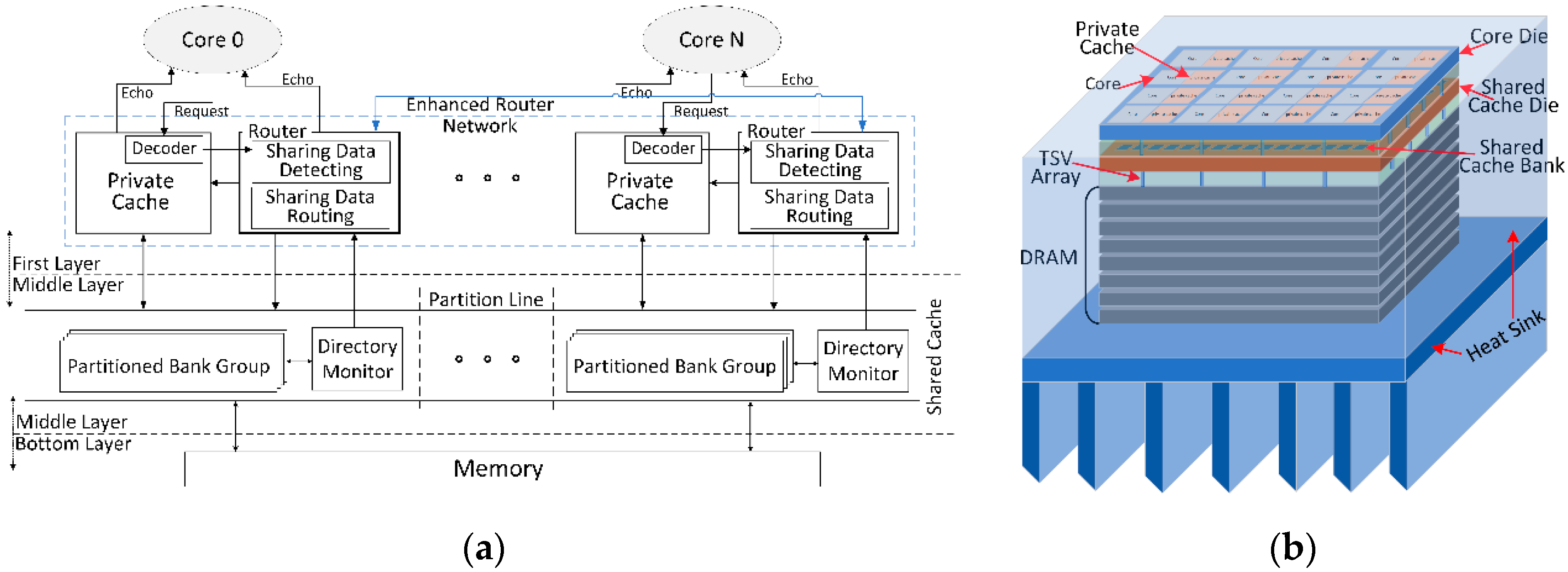
The 3D stacked CMP architecture has a unique feature that it can separate high-speed cores and private caches, shared cache and low-speed DRAM memory into different layers. Thus, we are motivated to employ such 3D stacked architecture for rapidly solving sharing data of private cache accesses in the core layer rather than across layers, thereby saving plenty of data maintenance cycles. And the throughput traffic on the TSV array can be reduced greatly. Thus, a 3-layer 3D stacked architecture is employed as the base system.
As shown in Figure 2a, the only hardware difference between base system and our proposed system is that in each private cache of our proposed design is integrated an enhanced router for detecting and routing sharing data. The shared L2 cache is maintained by MOESI_CMP_directory coherence protocol from Gem5 simulator [7], and write back strategy is employed. In order to explain architecture setups well, we make five key assumptions as follows:
- The shared cache is partitioned into several bank groups while each partitioned bank group only directly link to one private L1 cache and one processing core in the up-layer (like 2D dance-hall structure). In this work, we employ directory-based coherence protocol into the shared L2 cache for migrating sharing data among partitioned bank groups.
- The parameter of temperature has a profound influence on the static power and working condition of layout cells. Thus, we set the temperature parameter as a design constraint. During simulation tests in Gem5 platform, the static power is achieved by averaging seven overall static power values which are severally simulated under the temperature of 25 °C, 35 °C, …, 85 °C.
- Data interconnection between two layers relies on TSV arrays. As shown in Figure 2b, each private cache interlinks its partitioned bank group via a TSV array. Based on TSV modelling in [8,9], we assume that the request data can pass through the TSV array in a constant latency of 0.1 ns and 1.62 pJ/bit energy, while no delivering congestion and inaccuracy happen.
- Overheating issue in 3D stacked architecture acts as a key design challenge. As shown in Figure 2b, a 3D stacked 16-core 3-layer architecture is packaged in the heat sink. We consider two methods to solve this issue that one is an external cooling method by filling cooling materials between layers and imbedding the chip in heat sink, the other one is an internal cooling method by dynamically managing overheated chip components cooled down [10]. As shown in Appendix A, we conduct the thermal simulation to reveal that all chip components are working under a certain temperature constraint.
- The layout design of the base system refers to previous work in [11]. As shown in Appendix A, the area values of each layer are evaluated to assume that the design areas of all stacked components are suitable to pile up in the heat sink.
2.2. Re-Define Access Patterns of Private Cache
All private cache accesses, including read and write accesses, can be classified into seven access patterns based on where the target data of current access request is located, and each access pattern is described as follows:
- Pure Miss Accesses (PM-A). The target data of private cache access do not exist in both the private cache of the current thread and the private caches of other threads. For example, consider that Core0 requests to load or write DataX into its private cache, and all private caches, do not contain previous DataX. Thus, the pure miss accesses can be handled by loading DataX from shared cache or writing through DataX to cache hierarchy.
- Shared Write Accesses (SW-A). The target data of write access on private cache exists in both the private cache of the current thread and some private caches of other threads. For example, consider that Core0 makes requests to write DataX into its private cache while previous DataX copies are existing in the private cache of the current thread and also in the private cache of CoreN’s thread. In conventional path, the DataX should be written to its partitioned shared cache banks and then the new DataX is updating to the cache hierarchy of CoreN’s thread with the aid of directory controller logic while consuming hundreds of clock cycles.
- Shared Read Accesses (SR-A). The target data of read access on private cache exists in both the private cache of the current thread and some private caches of other threads. For example, consider that Core0 requests to load DataX from its private cache while previous DataX copies are existing in the private cache of current thread and also in the private cache of CoreN’s thread. In the conventional path, the DataX can be directly read from its private cache.
- Crossed Write Accesses (CW-A). The target data of write access on private cache does not exist in the private cache of the current thread; however, previous DataX copies are existing in some private caches of other threads. For example, consider that Core0 requests to write DataX into its private cache while previous DataX copies are existing in the private cache of CoreN’s thread. Similar to the process of shared write accesses, the DataX should be written to its partitioned shared cache banks and then the new DataX should be updated to the cache hierarchy of CoreN’s thread with the aid of directory controller logic while consuming plenty of clock cycles.
- Crossed Read Accesses (CR-A). The target data of read access on private cache does not exist in the private cache of current thread; however, previous DataX copies are existing in some private caches of other threads. For example, consider that Core0 makes requests to load DataX from its private cache while previous DataX copies are existing in the private cache of CoreN’s thread. In the conventional path, such access will bring about a miss in its private cache or even a miss in its partitioned bank group (private L2 slice), thereby consuming many clock cycles to load DataX.
- Repeated Write and Read Accesses (RW-A and RR-A). The target data of any repeated access on a private cache only exists in the private cache of the current thread. For example, consider that Core0 requests to access DataX at its private cache while no previous DataX copies are existing in the private cache of other threads. In the conventional path, such access can be directly handled by hitting at the private cache of the current thread.
In essence, crossed read and write accesses will finally shift as shared access types after the target data are delivered to the private cache of the current thread. As a result, DataX is indirectly shared by two copies in private caches which serve to different threads. Meanwhile, each data modification by any core (i.e., CoreN) will lead to shared data asymmetry, and in order to keep data coherence, the modified DataX needs to a written update for all other copies or all other copies are written invalidated, but these two methods need sophisticated hardware to detect all copies and then update them across private caches and partitioned banks of shared cache [4]. It can be observed that there are no straightforward access paths among private caches, and even among different partitioned bank groups of the shared cache. Thus, shared data existing in different threads are difficult to be transported directly, and the coherence protocol needs to do complex and costly operations across those threads. Thus, we intend to bridge each thread for disseminating information through the router network in the first layer, which can be acting as a far faster access path rather than the path in virtue of directory logic or even off-chip memory.
As shown in Figure 2a, decoded requests from each core can be spread to the linked router and further to other routers with the aid of enhanced router network. Once any sharing data is detected, data interconnection from any thread to any parallel thread can be easily implemented by the meshed router network. Quite sensibly, the router can act as a fast data repeater among those parallel threads. In other words, the data requested from CoreN to DataX can spread from RouterN to Router0 and then return the target data through the router network if Router0 has already stored the DataX. Besides, if each router can record some previous data, subsequent requests from CoreN to DataX can be fleetly returned as long as one of the routers has a copy. Hence, the conventional router should be enhanced with the ability to firstly record some previous sharing accesses, secondly maintain sharing data and finally transport target sharing data. Note that the router can only buffer some frequently requested data rather than all data due to hardware and latency costs. As a consequence, the access distributions of all private cache access patterns should be counted for feasibility analysis on the potential promotion of handling those accesses, and those distributions are represented as follows.
2.3. Private Cache Access Distributions
In order to calculate the distributions among all private cache accesses, we employ PARSEC benchmark suite [12] to run on the test platform. During each test, we employ 16 copy caches for one by one recording all contents in 16 private caches dynamically. Any private cache access should explore all copy caches to check which copy caches it will hit. Thus, all private cache accesses are classified into seven groups corresponding to each access pattern.
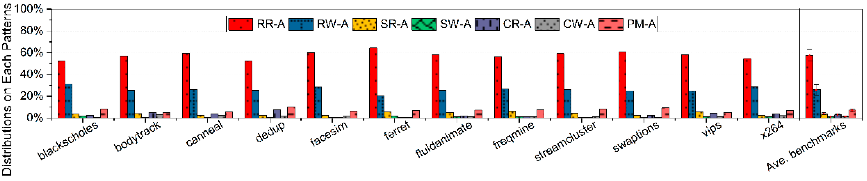
Figure 3 represents the hit distributions of each access pattern, where shared read and write accesses take up on average 3.82 percent and 0.95 percent of all private cache accesses, respectively. Typically in shared write accesses, the target data should be transported to other private caches for updating previous target data, and such processing path costs even a dozen times of clock cycles over the processing path on shared read accesses. Moreover, each shared read access acts as potential shared write access whenever there is a further modification on the shared data. Thus, shared read and write accesses retard the performance of data throughput in cache hierarchy.
In parallel computing threads, there are existing plenty of crossed accesses which are first identified as misses on the current thread and hits on other threads. Statistically, crossed read and write accesses can take up on average 2.98 percent and 1.31 percent of all private cache accesses, respectively. For a crossed read access, it tends to endure a miss on private cache or even partitioned bank group of shared cache in the conventional processing path, thereby consuming many cycles to load target data. For a crossed write access, the target data should be updated to relevant private caches of other threads while such updating process is similar to the one of shared write access. As a consequence, both crossed read and write accesses will bring about complex and costly operations in the conventional path, where extra misses and data non-coherence are concomitantly handled.
Hence, we are motivated to bridge all private caches for rapidly handling some harmful private cache accesses in a much faster way so that it is preferable to enable all private caches with data interconnecting ability by establishing an enhanced router network in caches. The network is enhanced with the ability of detection particular access, data replacement, and data transportation, whereby many harmful accesses can be rapidly handled. Ideally, target data of shared write accesses can be quickly updated to other private caches through the router network rather than the conventional processing path; Any modifications on the target data of shared read accesses can be easily spread to all appropriate destinations; The access misses in crossed read accesses can be rapidly handled by loading target data from other relevant private caches with the aid of proposed network; The new data generated in current private cache can be fleetly written to all related caches by means of bypassing target data across the network. As a consequence, the private caches integrated with proposed router network can achieve significant improvement on access latency if some harmful accesses are relieved with the aid of this network. The design details of the network are described as follows.
3. Stacked 3D Router Network Design
3.1. Base Router Design
In this work, the proposed router only delivers a number of sharing data and repeated read and write data which are existing at its history buffers. Thus, the main requirement of router design is to sacrifice some throughput performance for a very small integrating scale, unlike throughput first in conventional routers [13]. Thus, we make a tradeoff decision on buffer and Virtual Channel (VC) scales. Our five-port router supports fifty flits of buffering operation (65-bit flit, one packet contains five flits), and those flits are allocated to five VCs where each VC serves to two input buffers of each port. Under the design constraint of requested throughput (guarantee a maximal flow of sharing data), the above decisions on allocating input buffers to VCs are set as minimal hardware overhead. For the VC allocator, we build a free VC table and a reserved VC table to arbitrate VC occupations.
3.2. Router-integrated Cache Architecture Design
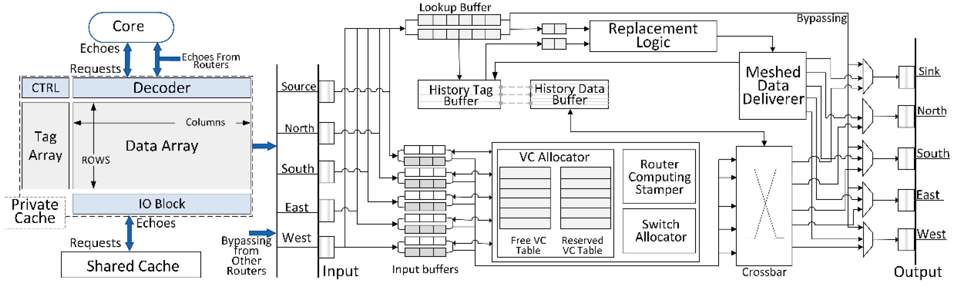
Figure 4 represents the router-integrated cache architecture, which consists of conventional up-down core-private cache-shared cache structure and enhanced router structure. The core sends out access requests including write and read accesses to private cache, and once the address information (i.e., tag bits) of any access request is decoded in the private cache, such information is concurrently employed for exploring in the private cache and as well as delivered to the lookup buffer of linked router for exploring previous existence location of target data among entire router network. Thus, in case of write access, the new target data can easily be written to any previous location through transporting within router network, and in case that read access encounters a miss on private cache, the target data can be loaded from any previous location with the aid of router network.
To proceed with cache accesses efficiently, proposed router architecture is enhanced based on a previous router design [13]. Based on the base network architecture, our proposed design supports three extra functions as follows:
- Target accesses exploration. Our proposed router is integrated with history data buffers for saving the recent private cache accesses, and any decoded request can explore in the lookup buffer (only records several entries) and further this request is spreading in the router network for detecting all previous accesses. If there is an access request sent to a router, two concomitant access mechanisms are triggered—one is to deliver the access package to the next layer inconsistent with conventional routing path, the other one is to spread the access request in the router network to explore whether the history buffer of current router contains the previous target data, or whether the history buffers of other routers contain the previous target data. Thus, such request can be identified to mark any crossed access or shared access out. Furthermore, this access request can be efficiently handled through redesigned processing path corresponding to each access type.
- Data replacement. The history buffer should be updated with the recent access results, and furthermore, some current results will be retired based on the Least Recently Used (LRU) replacement algorithm. Concerning each alteration on the history buffer of one router, altered data should be spread into four locations: private cache, the partitioned bank group connected to this router, the history buffers of other routers which contain the shared target data, and further both private caches and partitioned groups linked to other routers.
- Data delivery. The data deliverer is proposed to selectively export both target data and tag information to different destinations concurrently. Firstly, the data delivery should support echo target data back to the linked core. Meanwhile, any sharing data should be updating all related copies for data coherence, and any address information should be fleetly bypassing all other routers [14]. Finally, stored history data should be retired out old data and also be updated with new data.
To sum up, the proposed routers can be featured in a concurrent path. As the conventional shared cache access path (including data routing path) is much longer over the concurrent processing path, access latency on many filtered accesses can be significantly shortened. Moreover, the proposed routing path only works well when each access type can be detected fleetly, in addition to handling them in very few cycles. Thus, we propose a novel router architecture based on the above function descriptions, and the router hardware will be described in the next subsection.
3.3. Enhanced Router Architecture
The routing pipeline of our proposed router is formed based on the conventional routing path, where the enhanced path and conventional path are integrated to work concurrently. The enhanced path contains three key components which demonstrate one to one correspondence to the function descriptions in the last subsection, and the internal details of each component are depicted in the subsequent subsections.
3.3.1. Target Explorer Design
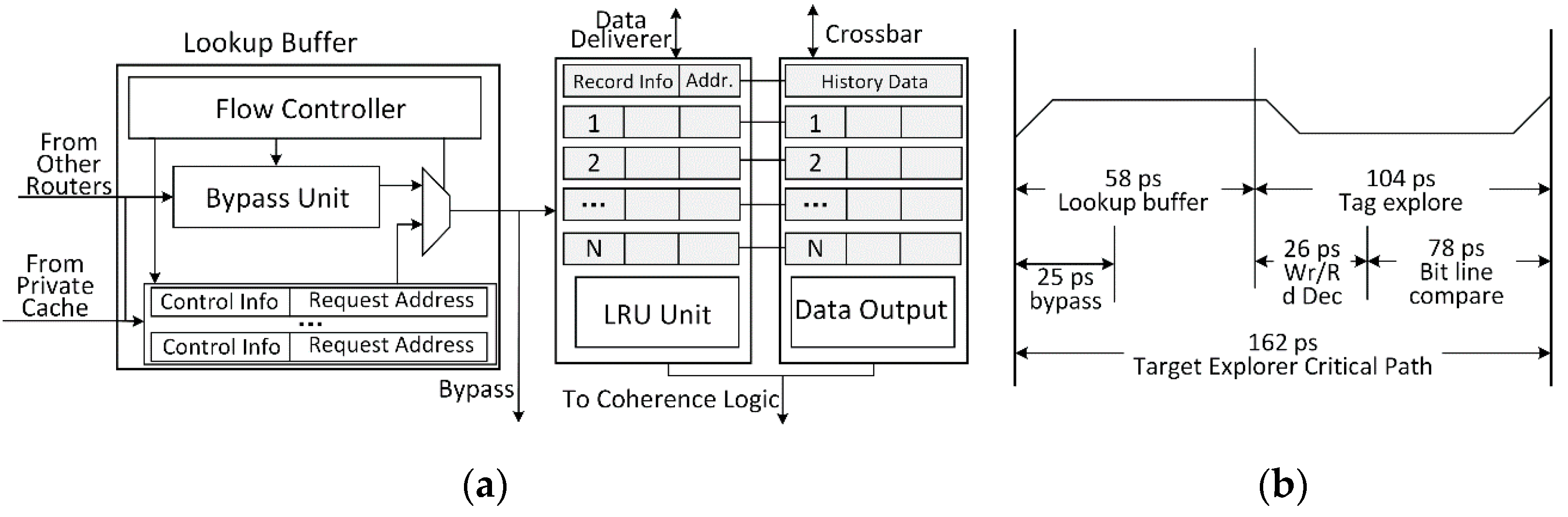
Figure 5a represents the Target Explorer (TE) architecture, which is employed to handle two kinds of data inputs from the linked private cache and other routers [6]. For each decoded request from private cache, the address information is compared with a tiny but fast lookup table (i.e., four entries) to detect prior accesses, and concurrently this address is spread forward to other routers through broadcasting across the routing network. Then, this address is further compared with the history tag buffer (maintained under LRU replacement policy) for exploring previously-stored target data which had been identified as sharing data, and if there is a hit on the current buffer, the last target data can be rapidly echoed to the processing core unit (Read access), or the new target data can be written to the history data buffer and further to other related routers (Write access). In case of a miss on current buffer but hit on other routers, the target data can be loaded from other routers or the new target data is written to other routers. Otherwise, if any sharing data misses at history buffers, this data will be maintained by the directory logic of the shared cache, and further this data will be loaded to update history buffer. Once a target data is detected as sharing data, this data will be saved in the history tag and data buffers. Additionally, those buffers only store the latest access results which are generated from any concurrent access detected in lookup buffers or are echoed from directory monitor of shared cache. Furthermore, the retired sharing data will be delivered to data replacement logic to update all related copies in the router network.
Figure 5b describes the approximate critical path latency of target explorer logic, where each latency is counted by calculating the access delay from source_CLK to sink point of each component in the IC Compiler. The address information of private cache accesses can bypass across the target explorer within 25 ps, and further can arrive at all routers by three times routing on an interlinked4x4 router network. Concurrently, such address information needs to explore in the lookup buffer and then is controlled to output within 58 ps. Furthermore, this information will be compared to the history tag buffer for identifying previous sharing data with 104 ps. The longest critical path of target explorer consumes 162 ps latency while the most prolonged latency of identifying one access from the time point of request address arriving to the end of finishing target exploration in the outermost router can be calculated as n times bypass * (25 + 17 output latency) + 162 = 162+42n ps (n stands for the router number of bypassed routers), which is far less than the latency of private cache access.
3.3.2. Data Replacement Design
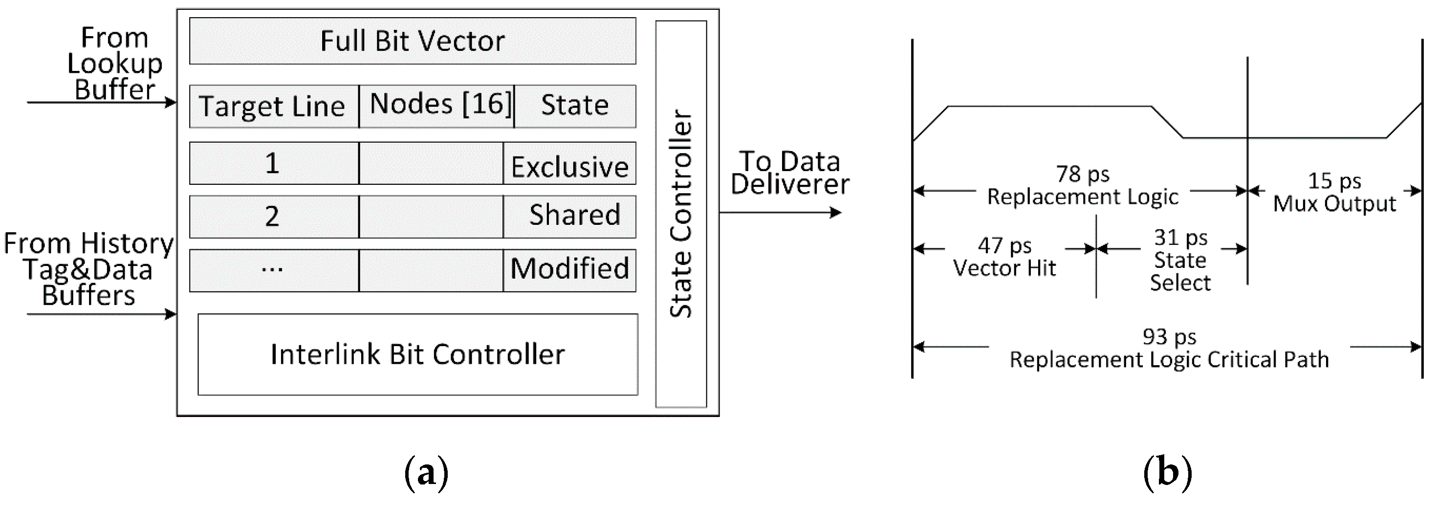
Figure 6a shows the internal architecture of Data Replacement (DR) logic [6], which is designed for maintaining data coherence on detected sharing data. In case of detecting sharing data in lookup buffers, this data will be loaded into history buffers with shared state, and further several extra bits are generated to link related routers. Meanwhile, each tag address should search for the history tag buffers across router network and any hit on those buffers will trigger data replacement check for data coherence. Moreover, the sharing data which are detected by the directory-based coherence logic of shared cache will be echoed to private cache and history buffers of related routers, and further, those data should import to data replacement logic for integrating extra interlink bits. Finally, marked address information should be sent to data deliverer for also updating sharing data on related routers. Figure 6b represents the critical path latency of DR logic. The address information of sharing data will be exploring to the directory within 78 ps, and then the state transition is conducted within 15 ps. Counting in the output latency, the overall latency of data replacement path is about 93 ps.
3.3.3. Data Deliverer Design
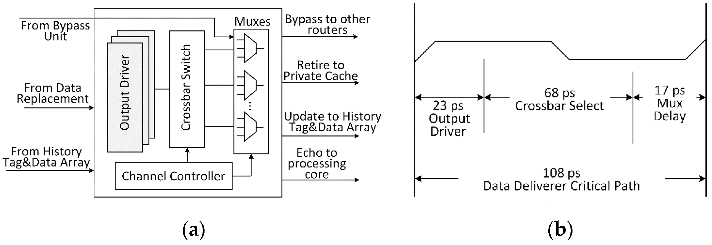
Figure 7a shows the internal architecture of Data Deliverer (DD) logic [6], where the crossbar switch is extended from the crossbar of the conventional router. The DD logic can handle three kinds of input data, including bypass data, treated shared data, and retired history data. As the bypass data need to be quickly spread to all routers, the DD logic is designed to directly export those data by Muxes logic while the output delay is about 17 ps. Moreover, treated shared data will be selected to echo back to the processing core or bypass to other routers based on output signals of the channel controller. As to retired data from history tag and data buffers, they will be sent to private cache and further to the shared cache for data coherence. Especially, the target data delivered from other routers to the current router, which have been handled by DR logic, should be updating to history tag and data buffers by data switching. Figure 7b shows the critical path latency of DD logic. The data can be bypassed within 17 ps. Meanwhile, the output data can be driven to the crossbar for data switching within 68 ps, and then those data are driven to export within 23 ps, thereby the overall latency of DD path is about 108 ps.
3.3.4. Coherence Protocol Modifications.
Beyond the baseline coherence protocol of MOESI directory, we only do modifications on two situations: a) Updating the already-handled sharing data from the first layer until to memory; b) Retiring sharing data from L1 cache level. In the first situation, if a write request to sharing datum is handled in the first layer, the cache line state in requester’s L2 slice should be changed to ‘Owned’ state and state in sharer’s L2 slices are changed to ‘Shared’ state. If a read request to sharing datum is handled in the first layer (i.e., a crossed read access), the cache line state in both requester’s L2 slice and other sharer’s L2 slice should be changed to ‘Shared’ state. In the other situation, if the cache line of a sharing datum is retired from L1 cache level, relevant cache line state in its L2 slice should be changed to ‘Shared’ state.
3.4. Routing Path and Topology Design
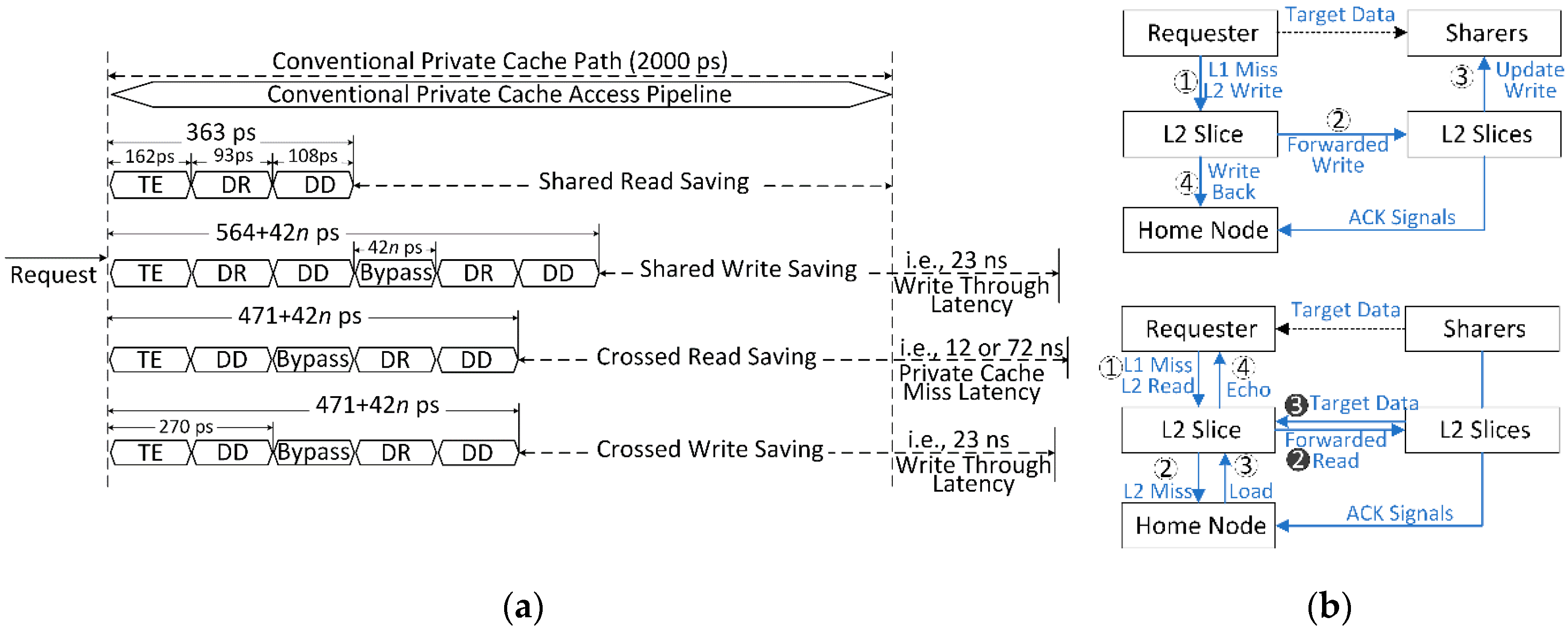
In this section, the routing path details of proposed router network are depicted, and also the potential latency savings of each path are calculated corresponding to each access type of detected private cache accesses. As shown in Figure 8a, four access types, including shared read/write and crossed read/write accesses, are handled in the proposed path as follows:
- Shared read access. For shared read access, its address information will be spread in the router network, and then the previous read can be detected in TE stage within 162 ps. Then, the target data stored in history tag buffer should be sent to DR logic for marking interlink bits within 93 ps. Finally, the current DD logic will export the target data to processing core within 108 ps. As a result, the shared read access can be handled with 363 ps, which is far less than the latency of the conventional path
- Shared write access. Once shared write access arrives, its address information will be spread in the router network for locating previous target data addresses at history tag buffers of both other routers and current router while those operations are done in TE stage. Then, the address of this write access should be sent to DR logic for marking interlink bits. Thus, the current DD logic will export the target address and related data to the present history tag and data buffers. Meanwhile, the target data of this write access will be bypassed to the relevant routers, and further, the target address of this write access marked with interlink bits should be sent to DR logic. Finally, both target address and data will be exported to update the last target data stored in history tag and data buffers of related routers and furthermore update the previous data existing in the private caches corresponding to those related routers. As a result, the new data of shared write access can be easily replaced to all old data existing in different threads within 564 + 42n ps rather than the significant latency (approximate to 23 ns) of writing through processing threads
- Crossed read access: In conventional path, a crossed read access will miss in private cache and also possibly would get missed in partitioned shared cache banks, thus, a shared cache access is required with about 12 ns latency, or even an off-chip memory access costs approximately 72 ns latency, or a series of complex directory matching operations are needed to handle this access. However, in the proposed path, the address information of this access will be explored in lookup buffer and current history tag buffer in TE stage. Meanwhile, such address information will be directly exported in DD logic, and then that information will be bypassed across the router network for detecting previous read data existing in other routers. Following that, the target address will be sent to DR logic, and subsequently, the target data will be exported to the current router in DD logic. Finally, the target data can be echoed to the processing core, and the history tag and data buffers of the current router will be updated with the borrowed data from other routers. As a result, the crossed read access can be handled within 471 + 42n ps, which is far less than the latency of the conventional path
- Crossed write access: The address information of crossed write access will be firstly spread in the router network for locating previous target data addresses at history tag buffers of other routers in TE stage. Then, the address of this write access should be sent to DR logic for marking interlink bits. Thus, the current DD logic will export the target address and related data to the present history tag and data buffers. Meanwhile, the target data of this write access will be bypassed to the relevant routers, and further, the target address of this write access marked with interlink bits should be sent to DR logics of other routers. Finally, both target address and data will be exported to update the previous target data stored in history tag and data buffers of other routers, and also, to update the old target data existing at private caches. Hence, the new data of shared write access can be easily spread to replace the last data living in other threads with the latency of 471+42n ps rather than the significant latency (approximate to 23 ns) of writing through processing threads
Figure 8b represents sharing data read and write examples. For a detected access, target data can be allowed to route between sharers and requester. Thus, complex and expensive steps routing in low cache level can be saved. As those access types take a portion of private cache accesses by on average 3.82 percent, 0.95 percent, 2.98 percent and 1.31 percent, respectively, many potential improvements can be achieved because the access latency on handling detected sharing data in proposed path is dozens of times less than the latency in conventional path. Moreover, the meshed XY routing topology is employed with our 4x4 router network, where routing data in the horizontal direction have high priority, and the data in vertical direction contain low priority. In the case of a many-core situation, other routing topologies are selectable on the proposed router network, which is beyond the scope of this work.
Moreover, the proposed router network can only detect a portion of sharing data accesses as there is a trade-off between integration scale and working speed on history tag and data buffers. Thus, the quantity of buffer entries is preferable under the principle of the highest Instructions Per Cycle (IPC) won. As to sharing data access misses in the router network, the directory controller of the shared cache will be triggered to handle those accesses and further, the handled target data will be saved into related history tag and data buffers for data reuse.
4. VLSI Implementation
4.1. Setups on Router Architecture Layout
Our proposed router architecture is implemented through a series of operations including Verilog modeling, timing analysis in ModelSim 10.4, synthesis and implementation with IC Compiler, which employs process as our previous work [6]. Based on CACTIv6.5 cache model [15], we use sixteen 32KB caches as the private cache and a 16MB/128 bank cache as the shared cache in a 16-core platform. Meanwhile, the proposed router architecture is enhanced based on the conventional router design [13], and all input and output ports of the proposed router are described as follows:
- Target Explorer. 45-bit address hits in lookup buffer. The record entry table receives 69-bit address (45-bit address, 8-bit flow control, 13-bit interlink bits including 4-bit coherence bits and 3-bit miss status) from data deliverer, and retires 69-bit address to the replacement coherency logic. The linked data buffers also exchange 256-bit data blocks in step with the history data buffer.
- Data Replacement. Both detected shared data and retired data are handled to be transported to the data deliverer at 69-bit address length and 256-bit block length (325 bits in total).
- Data Deliverer. The deliverer allows data output to the network or updates linked history buffers at 325-bit length, and exports data to the current thread at the 301-bit length.
4.2. Area, Power and Latency Reports
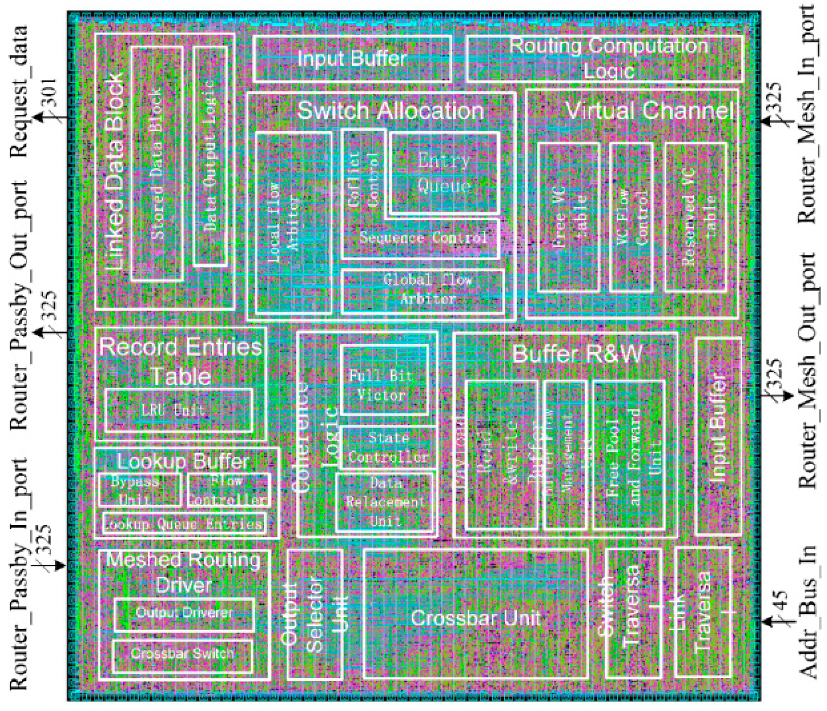
Figure 9 represents the physical design, in which critical components of the router are highlighted with frames to show their probable area details. As shown in Table 1, the proposed router contains 2237 ports, and there are 153944 gates counted in a five-level logic frame while those gates occupy approximately 0.68 mm2 design area and consume about 48.61 mW dynamic power and 5.17 mW leakage power. As to access latency, the longest path in the router is counted as 0.262 ns under 2865 clock sinks. When the router is tested to route a vast amount of no-load data, the maximum throughput speed in the proposed router can reach at 1.37 Tbits/s at 10 percent activity under 2.0 GHz clock frequency.
Compared to a 32 KB private cache [15], the design area of our proposed router only takes up about 8.93 percent area overhead. Furthermore, compared to a recent-released commercial chip named Intel Xeon E5-2683v4 (14 nm) which has 16 cores, 45 × 52.5 mm2 package area and 120 W power as an example [16], the overall area overhead of 16 proposed routers is about 16 × 0.6815 = 10.9 mm2, which takes up 0.58 percent of the on-chip area (assume package ratio of intel chip as 1.25). And the overall power overhead of those routers is about (48.6053 mW + 5.1749 mW) × 16 = 0.86 W, which takes up 0.72 percent of the on-chip power. As a consequence, the hardware overhead of our proposed router is small and insignificant compared to on-chip integration scale.
Moreover, the relationship between the integration scale of the history buffer and performance of the proposed router is investigated as follows. In case of small buffer scale, it has small access latency but can only detect a small amount of sharing accesses; however, in case of large buffer scale, it can detect a large amount of sharing accesses but handling each sharing access in proposed router costs significant access latency. Thus, the access latency values of history buffer whose size ranges from 16 entries to 1K entries are calculated through counting the access delay from source_CLK to sink point of history buffer hardware in IC Compiler. As shown in Table 2, the latency values are rapidly increasing along with the allocated entry scale, where 16-entry buffer only has 97 ps access latency, but 1K-entry buffer contains the insufferable access latency of 476 ps. As a consequence, there is a trade-off existing on allocating the optimal scale of the history buffer, which can be set as 32 entries based on performance and energy consumption evaluations described in the next section.
5. Experimental Evaluation
5.1. Platform Setups
Simulation platform: The accurate gem5 simulation model is employed to form a 16-core simulation platform which has three on-chip layers [7]. Table 3 lists the detailed parameters of processing cores, private cache, shared cache, off-chip memory and router architecture. As to the private cache and shared cache, they are established based on the CACTI cache model [15]. Furthermore, the simulator can integrate PIN tool for tracing instruction-driven simulation flowing in each customized model, thereby both performance and energy consumption values can be rapidly calculated in detail [17].
Router model: The layout results including path latency, area and power details are integrated into the conventional router architecture for establishing the enhanced router based on mesh_XY topology. As the integration scale of history tag and data buffers is highly related to the number of detected accesses (more massive size, more accesses detected) and also the latency of handling each access, seven kinds of entry numbers including 16, 32, 64, …, 1K entries are simulated for selecting the optimal scale based on the overall on-chip performance values.
Benchmarks: The PARSEC benchmark suite covers up different application domains and supports large-scale multi-threaded simulations [12], meanwhile its contained benchmarks have large working set, diverse locality and data sharing. Thus, those benchmarks are suitable to be our simulation workloads. During the simulation, each workload is allocated to sixteen threads while each processing core contains only one thread. Moreover, the initial one billion dynamic instructions are skipped for warming up, and the next ten billion dynamic instructions executed in all threads are counted uniformly for fair evaluations.
Comparisons: All values of the proposed system on throughput, performance and energy should be normalized with related values of the base system for the purpose of revealing improvements. Meanwhile, values of the base system with 64KB private cache size is compared with related values of base system to represent some improvements on allocating larger private cache, and the values of Proactive Resource Allocation (PRA) mechanism which acts as a related work over the proposed system are compared with related values of proposed system [18].
Evaluating metrics: In order to normalize the performance speedup and energy saving across those methods, three evaluation metrics defined as private cache throughput, speedup IPC and energy consumption are employed for counting runtime details during the period of executing fixed ten billion dynamic instructions, mean that each simulation test should start when the first one billion dynamic instructions are skipped, and the simulation must be stopped if the amount of dynamic instructions executed in all threads reaches ten billion dynamic instructions. Equation (1) represents the average throughput of private cache accesses, which is defined as the average number of handled private cache accesses counted in each thread per second (N stands for the number of concurrent threads). Equation (2) represents the speedup IPC metric, which is defined as the average IPC meant among all parallel threads, and Equation (3) shows that each energy consumption value calculated through counting overall energy consumed by all on-chip components during the period of executing ten billion dynamic instructions.
5.2. Experimental Results
Throughput improvement: To represent the throughput variations among benchmarks, Table 4 describes the average throughput values of private cache accesses within the base system and proposed systems with different history buffer entries. For different benchmarks executed in the base system, their throughput values range from 43.5 Gbps (dedup) to 120.7 Gbps (swaptions) while the average throughput value among all criteria is about 77.1 Gbps. Once the proposed router network is applied into the simulation platform, throughput values in all benchmarks are improved greatly, and the average value is about 100.5 Gbps with 16 history buffer entries allocated, and in case of 32 entries allocated, the average value reaches the peak throughput by 117.9 Gbps which is improved by 52.92 percent over the one of base system. As the integration scale of history buffer entries is ranging from 32 entries to 1K entries, the average throughput improvement tends to be decreasing from 115.3 Gbps (64 entries) to 89.2 Gbps (1K entries). In case of 1K entries allocated, only 15.69 percent of average throughput has been improved over the one of the base system.
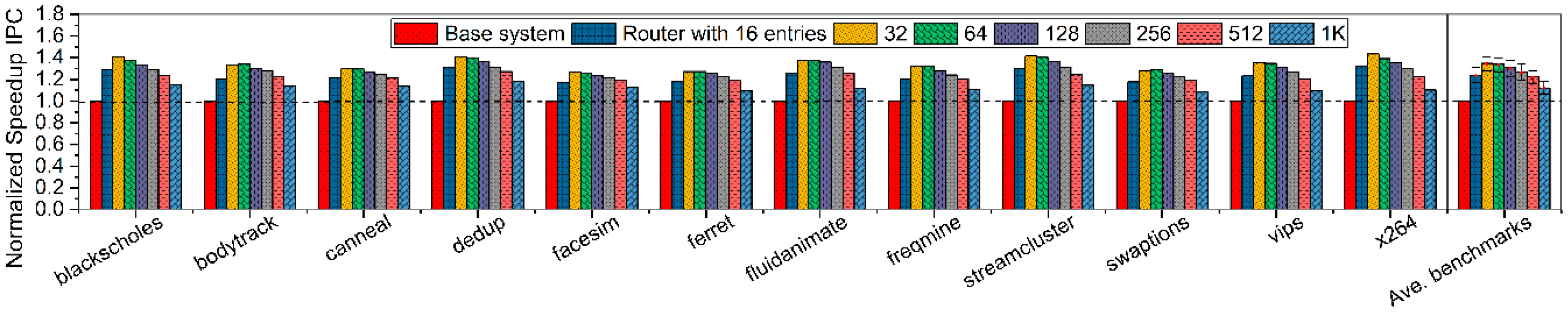
Performance improvement: Figure 10 represents the speedup IPC values while the history buffer scale of the proposed system ranges from 16 to 1K. Although there are 16 entries allocated to history buffer, proposed router-integrated system surpasses the base system in speedup IPC about 23.91 percent. When 32 entries are allocated to the history buffer, the average speedup IPC of proposed method outperforms the one of base system with the highest 31.85 percent. Then, the improvement on speedup IPC tends to be decreased along with allocated entries ranging from 64 to 1K, where 30.56 percent of speedup IPC improvement can be achieved by allocating 64 entries. However, in the case of allocating 1K entries, there is only 12.61 percent of speedup IPC improvement over the one of the base system.
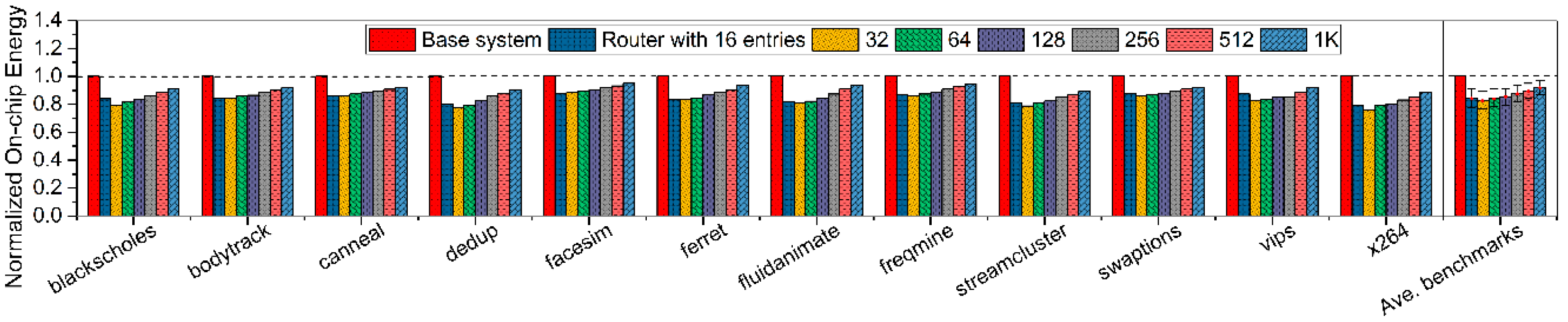
Energy-saving: Figure 11 represents the on-chip energy consumption values while the history buffer scale of the proposed system ranges from 16 to 1K. As all groups of simulation tests should be uniformed with the same amount of workload, each test on simulating any benchmark must count ten billion dynamic instructions during the executing period between the one-billionth instruction and the eleven-billionth instruction. Thus, the energy consumption of the proposed system can be improved over the one of base system, because that proposed system consumes far less executing time than the base system with the same workload. Experimentally, the energy values counted in our proposed system (allocated with 32 history buffer entries) can be saved about 17.61 percent over the ones of base system. Along with allocated entry scale increasing, the amount of energy saving tends to be decreasing from 15.93 percent (64 entries) to 7.85 percent (1K entries) over the base system.
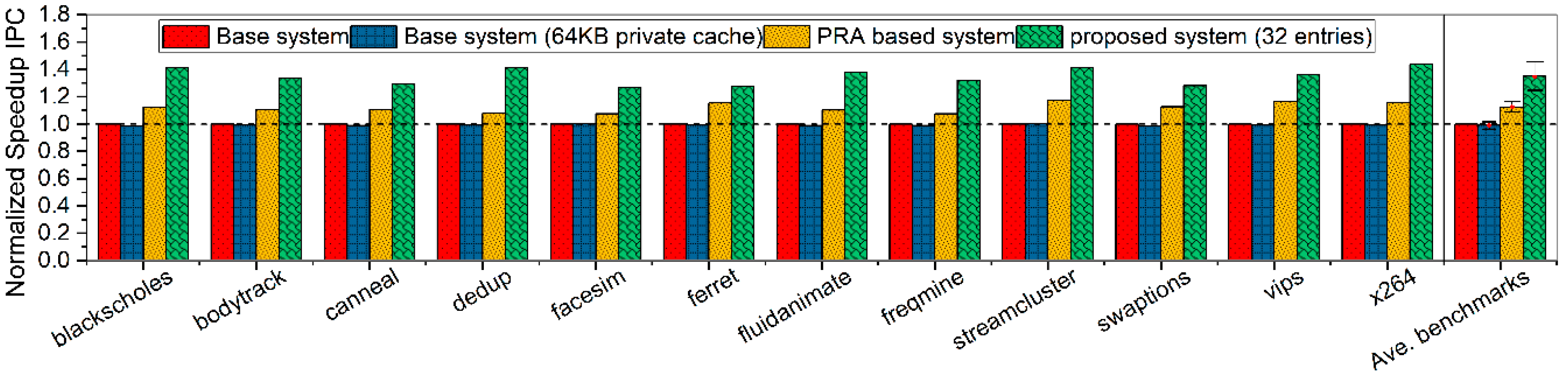
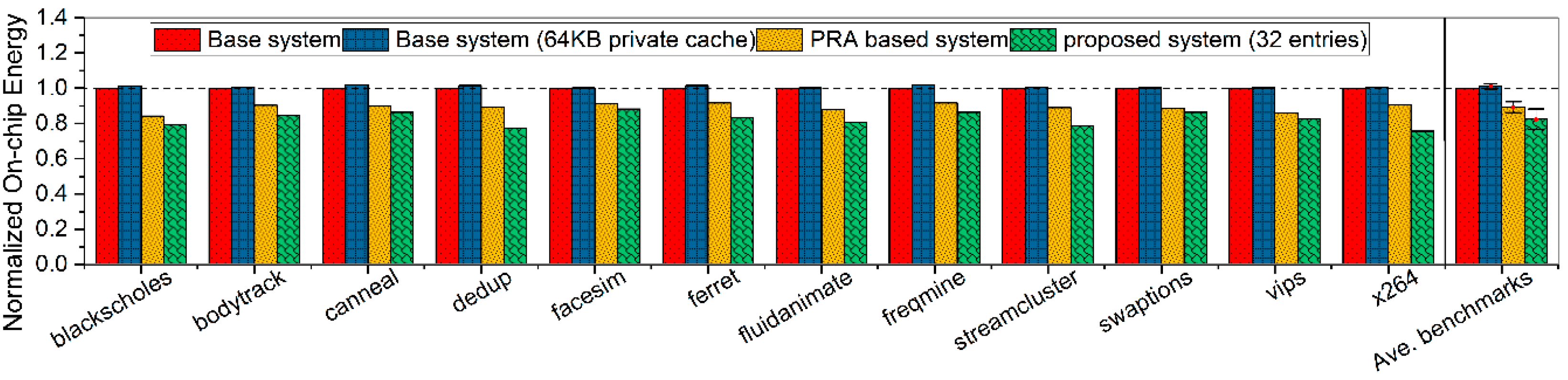
Related work comparison: Figure 12 represents the speedup IPC comparisons on four methods. And the PRA based system is compared with our proposed system (32 history buffer entries) to show significant improvement achieved by the proposed design. As the performance of private cache is highly related with the cache scale trade-off between hit rate and hardware cost, the speedup IPC values of the base system (64 KB private cache size) are marginally inferior to the values of the base system with an average of 0.82 percent. Meanwhile, PRA based system can achieve about 11.62 percent speedup IPC improvement. However, our proposed scheme can achieve about 31.85 percent improvement over the base system. Figure 13 represents the energy consumption values of those methods, where PRA-based system can save some on-chip energy by an average of 10.93 percent, while about 17.61 percent improvement is attained in the proposed system. However, allocating large private cache from 32KB to 64KB results in a proportion of 0.95 percent energy overhead. Note that PRA based system is necessitated to predict the cache accesses with extra hardware, and to predict precisely, this system requires a large scale of additional hardware which leads to the limitation of both speedup IPC improvement and energy saving in this system.
6. Discussion
Initially, two trade-offs on selecting the optimal private cache size and history buffer scale should be clearly discussed as follows:
- Trade-off on private cache size. As the hit rate of a private cache is increasing along with allocated cache size rising, the access latency of each private cache hit is also increasing as well. However, enlarging private cache size can gain some improvements only when the benefits from increased hits outperform the losses due to increased access latency. Moreover, large cache size will cost extra energy consumption on hardware overhead
- Trade-off on history buffer scale. With larger buffer scale allocated, more sharing data which are in larger reuse distance can be detected and further handled by router network. However, the enlarged scale will bring about extra latency on handling each detected sharing data. Similar to the former trade-off, the history buffer scale can also be enlarged when the benefits outweigh losses
Thus, the optimal private cache size can be tuned based on both speedup IPC and energy consumption comparisons, and 32 KB size is reasonably selected as the optimal one. Similarly, the history buffer scale can be determined as 32 entries based on the comparisons of private cache throughput, speedup IPC and on-chip energy consumption.
As described in Section 2.2, four kinds of access patterns, including shared accesses and crossed accesses together take up only an average of 9.06 percent of all private cache accesses. Moreover, both lookup buffers and history buffers can only detect recently reusable sharing data with limited hardware scale, and undetected accesses are handled by the shared cache. Thus, the amount of detected sharing data must be less than 9.06 percent of all private cache accesses, because that the history buffer scale is limited. However, for each detected access on shared data, the shared read access can be handled in the proposed router network within 363 ps rather than 2 ns latency of processing conventional read access. And shared write access can be processed within 564 + 42n ps (n ≤ 6 in 4 × 4 network) rather than 23 ns latency of a conventional write-through operation (up to 40 times faster). And crossed read access can be handled within 471 + 42n ps rather than 12 ns latency on processing shared cache access. And crossed write access can be handled within 471 + 42n ps rather than approximate 23 ns latency on processing a write-through operation. As a consequence, even if there are only small amount of shared data handled in the proposed router network, plenty of clock cycles consumed on those shared data can be saved considerably to a great extent with the proposed router network, thereby the throughput on a private cache is improved by 52.92 percent on average, and the speedup IPC is enhanced by 31.85 percent on average over the ones of the base system.
For fair comparisons, all simulation tests are unified to count the same amount of workload. Thus, the energy consumption with the proposed system can be reduced about 17.61 percent over the base system, due to the cause that, the execution time of the proposed system is far less than the base system even though the power of the proposed system is larger than the base system. The proposed system contains extra hardware overhead, but it is ignorable.
7. Related Works
The stacked 3D architectures flourishing in recent years tend to be the next generation on-chip architectures as they combine the good parts of parallel computation in CMP architectures and high-density integration in 3D architectures together. And emerging TSV techniques [3] actualize fast and wide, transferring bandwidths between layers in the vertical dimension. Thus, many researchers are motivated to employ stacked 3D architectures for easing the ‘Memory Wall’ issue in different angles. Some researches aim at boosting throughput performance by solving cache write overhead in 3D network level [1], or managing cache migration to reduce access latency [19]. Some researchers try to reduce energy consumption by applying the dynamic voltage and frequency scaling technique to manage the shared cache network [20], or proposing novel tree-based directory to bridge plenty of shared cache portions in 3D network [21]. The research in [22] proposed a novel narrow-width-value based stacked 3D cache architecture for both energy saving and yield improvement. The research in [23] tried to use thermal information in the shared cache to adaptively balance runtime status. Based on many mature 2D techniques, lots of attempts are propelling for the purpose of throughput performance, energy saving, thermal reduction and so on, implementing at the shared cache, private cache, router network or other combined on-chip components.
To simulate proposed designs precisely, cycle-accurate simulators are desired to build on-chip models. The updated SIMICS platform [24] can support the full system simulation with various instruction sets, but all built modules only can be plugged in this closed-source simulator integrally and unalterably. For open-source simulators, both MARSSx86 simulator [25] and Gem5 simulator [7] support cycle-accurate full system simulation, and the MARSSx86 simulator works well in particular CMP implementation. However, the Gem5 simulator integrates the excellent CMP simulator from M5 and the excellent cache memory simulator from GEMS together, which is suitable for studying cache network designs.
8. Conclusions
In this work, an enhanced router network is efficiently integrated into the private cache level for bridging parallel processing threads in the first layer of a stacked 3D on-chip system. The proposed router can rapidly detect all sharing data existing in different threads, and then those data can be maintained for data coherence by delivering target data across threads with the aid of a router network, thereby saving plenty of clock cycles on sharing data management. Moreover, the proposed router is implemented to evaluate a hardware overhead like area, power and integration scale. Resultantly, those overheads are ignorable. Finally, the simulation system integrated with the proposed router network can outperform the base system about 31.85 percent on the improvement of IPC and about 17.61 percent on the improvement of energy consumption.
Author Contributions
Conceptualization, H.Z. and W.T.; methodology, H.Z.; software, H.Z. and X.J.; validation, H.Z. and W.T.; formal analysis, H.Z. and X.J.; investigation, H.Z.; resources, X.J. and W.T.; data curation, H.Z.; writing—original draft preparation, H.Z.; writing—review and editing, H.Z. and W.T.; visualization, H.Z. and X.J.; supervision, W.T.; project administration, W.T.; funding acquisition, H.Z. and W.T.
Funding
This research was partly funded by the Science Foundation for Young Scientists of Jiangxi Education Department, grant number GJJ180486, and JSPS KAKENHI, grant number 18K11226.
Conflicts of Interest
The authors declare no conflict of interest.
Appendix A
The appendix consists of three parts: thermal evaluation of proposed 3D architecture, area evaluation of stacked 3D layers and area evaluation on TSV array.
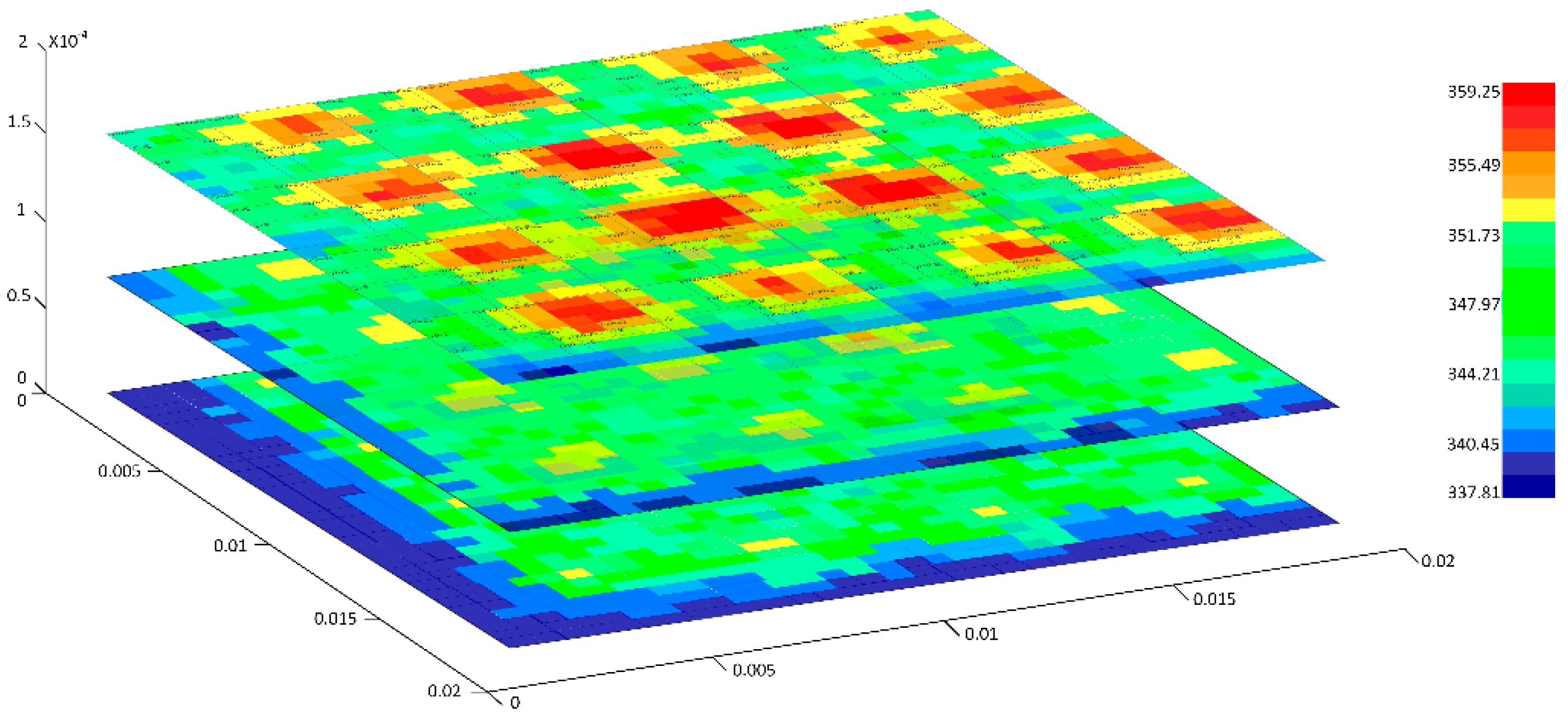
Thermal evaluation: in order to analyze the reliability under a thermal constraint, we employ the HotSpot 6.0 tool [26] for simulating proposed 3D architecture. Table A1 lists key parameter configurations in thermal models, and we achieve the trace power on three layers from Gem5 simulating platform and then insert to HotSpot tool for conducting grid model simulation. As shown in Figure A1, the steady temperature in three layers ranges from 337.81 K to 359.25 K which is lower than the temperature threshold of 363.15 K. Typically in the top layer, the processing cores contribute a lot of heat, where efficient heat dissipation methods are desired to apply in this layer.

Table A1.
Parameter configurations in HotSpot thermal model.
| Parameter | Value | Parameter | Value |
|---|---|---|---|
| Chip thickness | 0.00026 m | Specific heat capacity | 1.75 MJ/(m3-K) |
| Thermal conductivity (Si) | 110 W/(m-K) | Initial temperature | 328.15 K |
| Stacked layer number | 3 | Ambient temperature | 298.15 K |
| Heat sink thickness | 0.0039 m | Temperature threshold | 363.15 K |
| Thermal conductivity | 350 W/(m-K) | Model grid | 32 × 32 |
Figure A1.
Thermal profile of proposed 3D three-layer architecture (steady temperature evaluated, size scale in Meter, temperature in Kelvin).
Figure A1.
Thermal profile of proposed 3D three-layer architecture (steady temperature evaluated, size scale in Meter, temperature in Kelvin).

Area evaluation on layers—we summarize the core model from Gem5, cache and memory models from CACTI tool, router model from layout report and TSV model from previous work in [3,8,9]. As listed in Table A2, components stacked in each layer are evaluated. In the first layer, 16-core integration area can be calculated as 291.04 mm2. The middle layer occupies 153.61 mm2 and the bottom layer takes up 214.34 mm2. The area ratio among three layers is about 1.36:0.72:1. Moreover, the middle layer remains some margin area for further extending the shared cache scale.
Table A2.
Area evaluations on three stacked layers.
| Layer | Quantity | Value (mm2) |
|---|---|---|
| First layer | Core die | 9.29 |
| L1I+ITB | 3.47 | |
| L1D + DTB + W/RQu | 4.16 | |
| Router + TSVs | 1.27 | |
| Second layer | L2 tag + array + output | 79.49 |
| Directory logic | 35.17 | |
| Cache controller | 18.63 | |
| Router + TSVs | 1.27 | |
| Third layer | Memory (×4 stacked) | 194.02 |
| Router + TSVs | 1.27 |
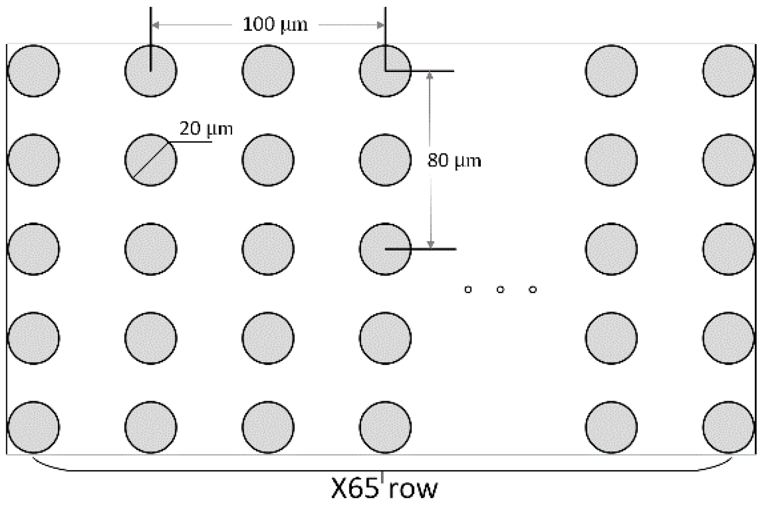
TSV area evaluation: our TSV array, which contains 5 × 65 TSVs, refers to the TSV model in [9]. Each TSV is set as 20 μm diameter and 80 μm pitch in scale, and those TSVs are distributing at the area shown in Figure A2. We can calculate the layout area of one TSV array to be 0.59 mm2.
Figure A2.
A 5 × 65 TSV array example, vertical pitch (80 μm) and horizontal pitch (100 μm) are set.
Figure A2.
A 5 × 65 TSV array example, vertical pitch (80 μm) and horizontal pitch (100 μm) are set.

References
- Mishra, A.K.; Dong, X.Y.; Sun, G.Y.; Xie, Y.; Vijaykrishnan, N.; Das, C.R. Architecting on-chip interconnects for stacked 3D STT-RAM caches in CMPs. In Proceedings of the 38th Annual International Symposium on Computer Architecture (ISCA), San Jose, CA, USA, 4–8 June 2011. [Google Scholar]
- Kim, N.; Ahn, J.W.; Choi, K.Y.; Sanchez, D.; Yoo, D.H.; Ryu, S.J. Benzene: An Energy-Efficient Distributed Hybrid Cache Architecture for Manycore Systems. ACM Trans. Archit. Code Optim. 2018, 15, 1–23. [Google Scholar] [CrossRef]
- Lu, T.T.; Serafy, C.; Yang, Z.Y.; Samal, S.K.; Lim, S.K.; Srivastava, A. TSV-Based 3-D ICs: Design Methods and Tools. IEEE Trans. Comput.-Aided Des. Integr. 2017, 36, 1593–1619. [Google Scholar] [CrossRef]
- Sadasivam, S.K.; Thompto, B.W.; Kalla, R.; Starke, W.J. IBM Power9 Processor Architecture. IEEE Micro 2017, 37, 40–51. [Google Scholar] [CrossRef]
- Gupta, S.; Zhou, H.Y. Spatial Locality-Aware Cache Partitioning for Effective Cache Sharing. In Proceedings of the 2015 44th International Conference on Parallel Processing (ICPP), Beijing, China, 1–4 September 2015. [Google Scholar]
- Zhao, H.T.; Jia, X.; Watanabe, T. Filter Router: An Enhanced Router Design for Efficient Stacked Shared Cache Network. IEICE Electron. Express 2019, 16, 1–6. [Google Scholar] [CrossRef]
- Binkert, N.; Beckmann, B.; Black, G.; Reinhardt, S.K.; Saidi, A.; Basu, A.; Hestness, J.; Hower, D.R.; Krishna, T.; Sardashti, S. The gem5 simulator. ACM SIGARCH Comput. Archit. News 2011, 39, 1–7. [Google Scholar] [CrossRef]
- Kim, J.; Pak, J.S.; Cho, J.; Song, E.; Cho, J.; Kim, H.; Song, T.; Lee, J.; Lee, H.; Park, K.; et al. High-Frequency Scalable Electrical Model and Analysis of a Through Silicon Via (TSV). IEEE Trans. Compon. Packag. Manuf. Technol. 2011, 1, 181–195. [Google Scholar]
- Kim, J.S.; Oh, C.S.; Lee, H.; Lee, D.; Hwang, H.R.; Hwang, S.; Na, B.; Moon, J.; Kim, J.-G.; Park, H.; et al. A 1.2 V 12.8 GB/s 2 Gb Mobile Wide-I/O DRAM With 4×128 I/Os Using TSV Based Stacking. IEEE J. Solid-State Circuits 2012, 47, 107–116. [Google Scholar] [CrossRef]
- Xiao, H.; Yueh, W.; Mukhopadhyay, S.; Yalamanchili, S. Thermally Adaptive Cache Access Mechanisms for 3D Many-Core Architectures. IEEE Comput. Archit. Lett. 2016, 15, 129–132. [Google Scholar] [CrossRef]
- Xiao, H.; Yueh, W.; Mukhopadhyay, S.; Yalamanchili, S. Multi-Physics Driven Co-Design of 3D Multicore Architectures. In Proceedings of the International Conference on Nanochannels, Microchannels, and Minichannels (ASME), San Francisco, CA, USA, 6–9 July 2015. [Google Scholar]
- Bienia, C. Benchmarking Modern Multiprocessors. Ph.D. Thesis, Princeton University, Princeton, NJ, USA, 2011. [Google Scholar]
- Ben-Itzhak, Y.; Cidon, I.; Kolodny, A.; Shabun, M.; Shmuel, N. Heterogeneous NoC Router Architecture. IEEE Trans. Parallel Distrib. Syst. 2014, 26, 2479–2492. [Google Scholar] [CrossRef]
- Guo, P.; Liu, Q.B.; Chen, R.Z.; Yang, L.; Wang, D.L. A bypass-based low latency network-on-chip router. IEICE Electron. Express 2019, 4, 1–12. [Google Scholar] [CrossRef]
- Muralimanohar, N.; Balasubramonian, R.; Jouppi, N.P. CACTI 6.0: A Tool to Model Large Caches. Available online: https://www.hpl.hp.com/techreports/2009/HPL-2009-85.pdf (accessed on 20 August 2019).
- Sodani, A.; Gramunt, R.; Corbal, J.; Kim, H.S.; Vinod, K.; Chinthamani, S.; Hutsell, S.; Agarwal, R.; Liu, Y.C. Knights Landing: Second-Generation Intel Xeon Phi Product. IEEE Micro 2016, 36, 34–46. [Google Scholar] [CrossRef]
- Luk, C.K.; Cohn, R.; Muth, R.; Patil, H.; Klauser, A.; Lowney, G.; Wallace, S.; Reddi, V.J.; Hazelwood, K. Pin: Building customized program analysis tools with dynamic instrumentation. In Proceedings of the 2005 ACM SIGPLAN Conference On Programming Language Design And Implementation (PLDI), Chicago, IL, USA, 12–15 June 2005. [Google Scholar]
- Lotfikamran, P.; Modarressi, M.; Sarbaziazad, H. Near-Ideal Networks-on-Chip for Servers. In Proceedings of the 2017 IEEE International Symposium on High Performance Computer Architecture (HPCA), Austin, TX, USA, 4–8 February 2017. [Google Scholar]
- Zhao, B.; Du, Y.; Yang, J.; Zhang, Y.T. Process Variation-Aware Nonuniform Cache Management in a 3D Die-Stacked Multicore Processor. IEEE Trans. Comput. 2013, 62, 2252–2265. [Google Scholar] [CrossRef]
- Chen, X.; Xu, Z.; Kim, H.; Gratz, P.; Hu, J.; Kishinevsky, M.; Ogras, U. In-network Monitoring and Control Policy for DVFS of CMP Networks-on-Chip and Last Level Caches. In Proceedings of the International Symposium on Networks-on-Chip (NOCS), Washington, DC, USA, 9–11 May 2012. [Google Scholar]
- Jung, J.; Kang, K.; Kyung, C.M. Design and Management of 3D-Stacked NUCA Cache for Chip Multiprocessors. In Proceedings of the 21st Edition of the Great Lakes Symposium on Great Lakes Symposium on VLSI (GLSVLSI), New York, NY, USA, 2–4 May 2011. [Google Scholar]
- Kong, J.; Koushanfar, F.; Chung, S.W. An Energy-Efficient Last-Level Cache Architecture for Process Variation-Tolerant 3D Microprocessors. IEEE Trans. Comput. 2015, 64, 2460–2475. [Google Scholar] [CrossRef]
- Clermidy, F.; Dutoit, D.; Guthmuller, E.; Miro-Panades, I.; Vivet, P. 3D stacking for multi-core architectures: From WIDEIO to distributed caches. In Proceedings of the 2013 IEEE International Symposium on Circuits and Systems (ISCAS), Beijing, China, 19–23 May 2013. [Google Scholar]
- Magnusson, P.S.; Christensson, M.; Eskilson, J.; Forsgren, D.; Hallberg, G.; Hogberg, J.; Larsson, F.; Moestedt, A.; Werner, B. Simics: A full system simulation platform. Computer 2002, 35, 50–58. [Google Scholar] [CrossRef]
- Patel, A.; Afram, F.; Chen, S.F.; Ghose, K. MARSS: A full system simulator for multicore x86 CPUs. In Proceedings of the 48th Design Automation Conference (DAC), San Diego, CA, USA, 5–10 June 2011. [Google Scholar]
- Zhang, R.; Stan, M.R.; Skadron, K. HotSpot 6.0: Validation, Acceleration and Extension. Univ. Va. Dep. Comput. Sci. 2015. [Google Scholar] [CrossRef]
Figure 1.
Processing cache paths of sharing data on conventional and proposed methods: (a) Classic CMP architecture; (b) Efficiency comparison between conventional path and proposed path.
Figure 1.
Processing cache paths of sharing data on conventional and proposed methods: (a) Classic CMP architecture; (b) Efficiency comparison between conventional path and proposed path.

Figure 2.
Proposed CMP system architecture: (a) Schematic diagram of enhanced router network; (b) an example of 3D stacked 16-core 3-layer architecture, where the chip is embedded in heat sink.
Figure 2.
Proposed CMP system architecture: (a) Schematic diagram of enhanced router network; (b) an example of 3D stacked 16-core 3-layer architecture, where the chip is embedded in heat sink.

Figure 3.
Access distributions on seven types of private cache accesses. All benchmarks are simulated to calculate distribution values by counted number in a pattern/all accesses.
Figure 3.
Access distributions on seven types of private cache accesses. All benchmarks are simulated to calculate distribution values by counted number in a pattern/all accesses.

Figure 4.
Proposed router architecture which is enhanced with three key components based on a conventional router [6,13].

Figure 5.
Architecture design on target explorer logic: (a) Hardware structure including lookup buffer and history tag and data buffers; (b) Critical path latency of target explorer when the history buffers contain 32 entries.
Figure 5.
Architecture design on target explorer logic: (a) Hardware structure including lookup buffer and history tag and data buffers; (b) Critical path latency of target explorer when the history buffers contain 32 entries.

Figure 6.
Architecture design on data replacement logic: (a) Hardware structure including full bit vector based directory logic and interlink bit controller; (b) Critical path latency of data replacement logic.
Figure 6.
Architecture design on data replacement logic: (a) Hardware structure including full bit vector based directory logic and interlink bit controller; (b) Critical path latency of data replacement logic.

Figure 7.
Data deliverer logic: (a) Hardware structure; (b) Critical path latency of data deliverer logic.
Figure 7.
Data deliverer logic: (a) Hardware structure; (b) Critical path latency of data deliverer logic.

Figure 8.
(a) Access paths of four access patterns including shared read/write accesses and crossed read/write accesses, while approximate access latency values of proposed path and conventional path are compared. Where 42n stands for the latency of bypassing n routers and n is less than or equal to six for XY routing in a 4 × 4 router network; (b) Data exchange examples on proposed path and conventional path, where dashed line stands for data routing in proposed network and dark-filled steps represent directory based coherence path.

Figure 9.
Layout of router architecture. Each components are marked with frames to show their on-chip compositions (not drawn in scale, this structure is built based on our previous work in [6]).
Figure 9.
Layout of router architecture. Each components are marked with frames to show their on-chip compositions (not drawn in scale, this structure is built based on our previous work in [6]).

Figure 10.
Normalized IPC values of proposed router-integrated system with different history buffer scales ranging from 16 to 1K entries.
Figure 10.
Normalized IPC values of proposed router-integrated system with different history buffer scales ranging from 16 to 1K entries.

Figure 11.
Normalized on-chip energy of proposed router-integrated system with different history buffer scales ranging from 16 to 1K entries.
Figure 11.
Normalized on-chip energy of proposed router-integrated system with different history buffer scales ranging from 16 to 1K entries.

Figure 12.
Normalized Speedup IPC comparisons among four methods, while our proposed system is allocated with 32 history buffer entries.
Figure 12.
Normalized Speedup IPC comparisons among four methods, while our proposed system is allocated with 32 history buffer entries.

Figure 13.
Normalized on-chip energy comparisons among four methods, while our proposed system is allocated with 32 history buffer entries.
Figure 13.
Normalized on-chip energy comparisons among four methods, while our proposed system is allocated with 32 history buffer entries.

Table 1.
Layout reports on integration scale, area and power details 1.
| Report Type | Quantity | Report Value (ICC) |
|---|---|---|
| Setups | Clock frequency | 2.0 GHz |
| Supply voltage | 1.1 V | |
| Temperature | 55 °C | |
| Technology library | 45 nm | |
| Integration Scale | Levels of logic | 5 |
| Number of ports | 2237 | |
| Cell number coun | 14189 | |
| Gate number count | 113944 | |
| Area Report | Combinational area | 0.2996 mm2 |
| Non-combinational area | 0.1182 mm2 | |
| Cell area | 0.4179 mm2 | |
| Net area | 0.2637 mm2 | |
| Design area | 0.6815 mm2 | |
| Power Report | Cell internal power | 31.1685 mW |
| Net switching power | 17.4368 mW | |
| Total dynamic power | 48.6053 mW | |
| Cell leakage power | 5.1749 mW | |
| Latency Report | Clock sinks | 2865 |
| Longest path | 0.262 ns | |
| CTBuffers | 729 |
1. The history buffer size is set as 32 entries.
Table 2.
Access latency values (ps) of history buffer with different entries allocated.
| Buffer Entries | 16 | 32 | 64 | 128 | 256 | 512 | 1K |
|---|---|---|---|---|---|---|---|
| Wr/Rd Decode | 26 | 26 | 27 | 29 | 33 | 43 | 59 |
| Bit Line Compare | 71 | 78 | 89 | 115 | 162 | 255 | 417 |
| Tag Explore Latency | 97 | 104 | 116 | 144 | 195 | 308 | 476 |
Table 3.
Parameter configurations on the simulation platform.
| On-Chip Component | Parameter Configurations |
|---|---|
| Processing Core | 2.0 GHz, 16 cores, single thread per core, 1.1 V supply voltage, 128 IW entries, 45 nm technology library, 30 cycle TLB miss latency. |
| Private Cache | 32KB for a core (private) including 16KB L1I cache and L1D cache, 4-way, 64 B line size, 4 cycle latency. |
| Shared Cache | 16 MB total size D-NUCA, 128 banks, 1 MB partitioned for a core (shared), 8-way, 128 B line size, 20 cycle latency. |
| Off-chip Memory | 4 GB Double Data Tate (DDR4 2133MHz, 1.2V), 8KB page size, 120 cycle latency. |
| Router Network | Mesh_XY Topology. 5 ports per router, 65-bit flit, 5 flits per package. |
Table 4.
Private cache throughput values of both base system and proposed system (Gbps stands for ×109 bits per second), where history buffer scale ranges from 16 to 1K entries 1.
Table 4.
Private cache throughput values of both base system and proposed system (Gbps stands for ×109 bits per second), where history buffer scale ranges from 16 to 1K entries 1.
| Benchmark\Sys. | Base | 16 | 32 | 64 | 128 | 256 | 512 | 1K |
|---|---|---|---|---|---|---|---|---|
| blackscholes | 70.8 | 96.5 | 111.5 | 107.2 | 103.6 | 97.9 | 91 | 80.5 |
| bodytrack | 82.6 | 104.6 | 125.9 | 123.8 | 119.5 | 112.1 | 104.7 | 95.8 |
| canneal | 62.9 | 82.6 | 99.1 | 93.7 | 90.4 | 85.6 | 80.9 | 73.2 |
| dedup | 43.5 | 62.1 | 79.7 | 75.1 | 71.8 | 67 | 62.3 | 56.7 |
| facesim | 83.7 | 101.1 | 122.5 | 119.8 | 114.5 | 105.9 | 99.7 | 89.2 |
| ferret | 63 | 81.7 | 95.6 | 93.4 | 90 | 86.3 | 80.5 | 71.2 |
| fluidanimate | 67.1 | 91.2 | 107.2 | 104.5 | 100.4 | 95.2 | 89.8 | 81.4 |
| freqmine | 92.1 | 116.5 | 135.5 | 134.5 | 129.8 | 124.3 | 118.4 | 106.8 |
| streamcluster | 71.8 | 98.5 | 114.1 | 113.2 | 109.3 | 103.9 | 95.7 | 83.9 |
| swaptions | 120.7 | 147.4 | 165.9 | 162.7 | 161.8 | 155.2 | 147.4 | 135.8 |
| vips | 88.9 | 114.2 | 131.3 | 129.6 | 125.2 | 120.6 | 113.8 | 103.6 |
| x264 | 78.2 | 109.6 | 126.2 | 125.8 | 121.7 | 107.2 | 100.3 | 91.4 |
| Ave. Value | 77.1 | 100.5 | 117.9 | 115.3 | 111.5 | 105.1 | 98.7 | 89.2 |
1. The proposed router only transports detected sharing data, so that the efficiency of proposed router is highly related on the history buffer scale, existing a tradeoff on detected data number and per-routing latency.
© 2019 by the authors. Licensee MDPI, Basel, Switzerland. This article is an open access article distributed under the terms and conditions of the Creative Commons Attribution (CC BY) license (http://creativecommons.org/licenses/by/4.0/).
Share and Cite
MDPI and ACS Style
Zhao, H.; Jia, X.; Watanabe, T. Router-Integrated Cache Hierarchy Design for Highly Parallel Computing in Efficient CMP Systems. Electronics 2019, 8, 1363. https://0-doi-org.brum.beds.ac.uk/10.3390/electronics8111363
AMA Style
Zhao H, Jia X, Watanabe T. Router-Integrated Cache Hierarchy Design for Highly Parallel Computing in Efficient CMP Systems. Electronics. 2019; 8(11):1363. https://0-doi-org.brum.beds.ac.uk/10.3390/electronics8111363
Chicago/Turabian StyleZhao, Huatao, Xu Jia, and Takahiro Watanabe. 2019. "Router-Integrated Cache Hierarchy Design for Highly Parallel Computing in Efficient CMP Systems" Electronics 8, no. 11: 1363. https://0-doi-org.brum.beds.ac.uk/10.3390/electronics8111363
Note that from the first issue of 2016, this journal uses article numbers instead of page numbers. See further details here.