Simulation-Based System-Level Conducted Susceptibility Testing Method and Application to the Evaluation of Conducted-Noise Filters

Abstract
:1. Introduction
2. System-Level Conducted Susceptibility Testing Standard
3. Proposed Simulation-Based Conducted Susceptibility Testing Method
3.1. BCI Probe Modeling
3.2. Calibration Jig Modeling
3.3. Noise Source Modeling
3.4. EUT Modeling
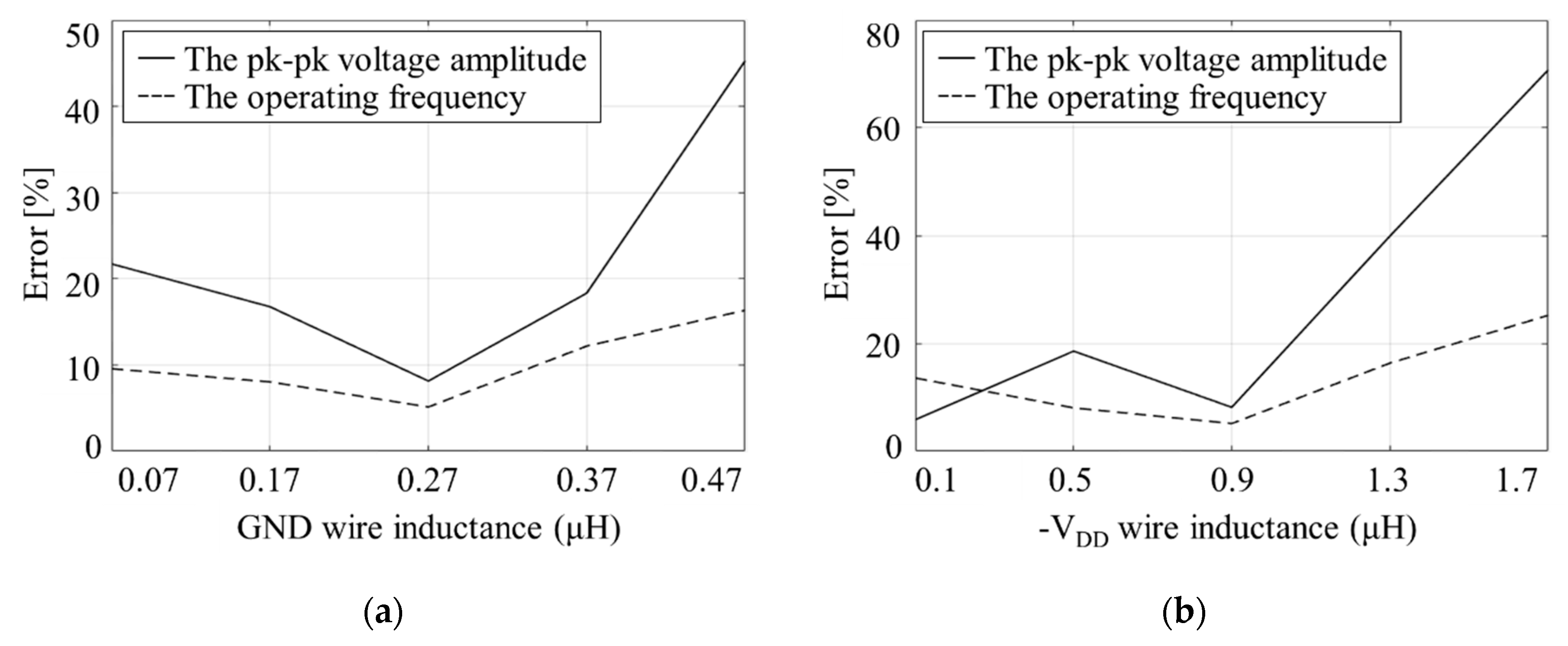
4. Experimental Verification
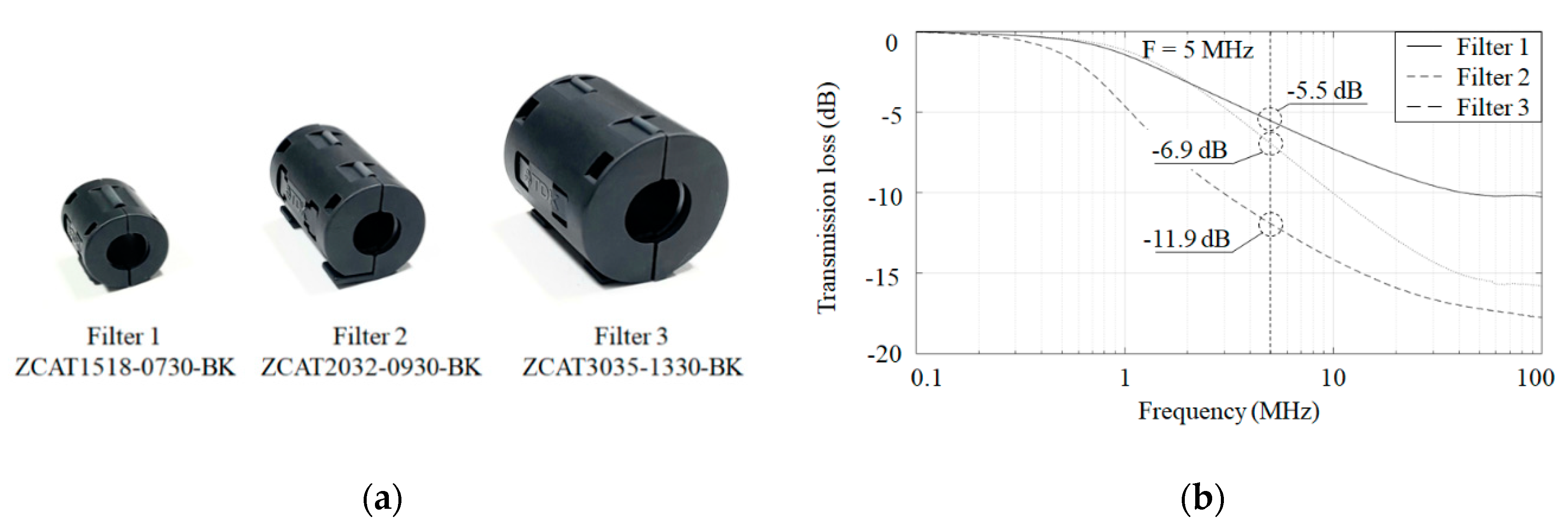
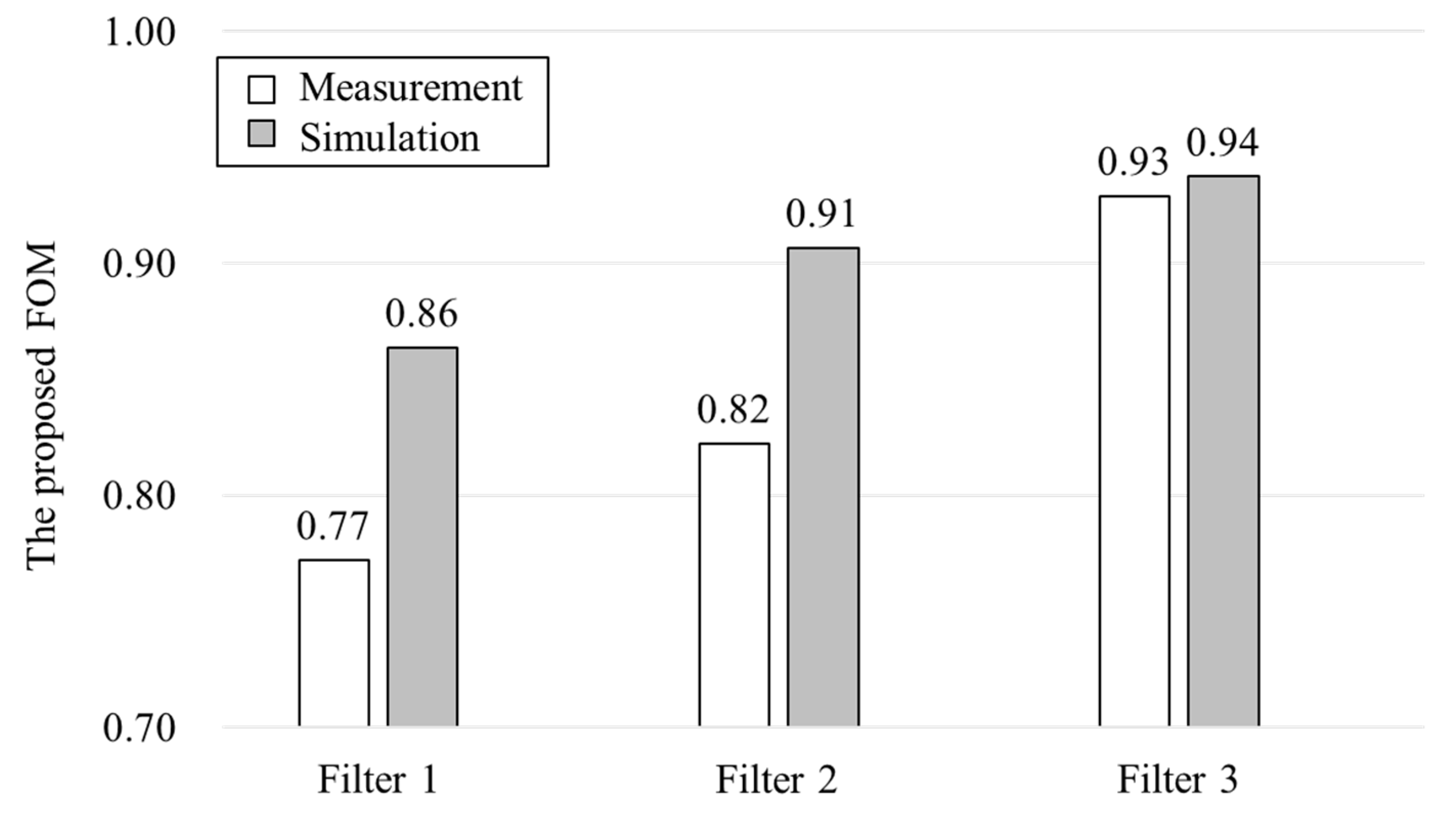
5. Application to the Evaluation of Conducted-Noise Filters
6. Conclusions
Author Contributions
Funding
Acknowledgments
Conflicts of Interest
References
- IEC. Integrated Circuits-Measurement of Electromagnetic Immunity, 150 kHz to 1 GHz-Part 3: Bulk Current Injection (BCI) Method IEC 62132-3; International Standard; International Electrotechnical Commission: Geneva, Switzerland, 2007. [Google Scholar]
- IEC. Electromagnetic Compatibility (EMC)-Part 4–6: Testing and Measurement Techniques-Immunity to Conducted Disturbances, Induced by Radio-Frequency Fields IEC 61000-4-6, 3rd ed.; International Standard; International Electrotechnical Commission: Geneva, Switzerland, 2008. [Google Scholar]
- Grassi, F.; Marliani, F.; Pignari, S.A. Circuit Modeling of Injection Probes for Bulk Current Injection. IEEE Trans. Electromagn. Compat. 2007, 49, 563–576. [Google Scholar] [CrossRef]
- Huynh, H.A.; Jo, J.; Nah, W.; Kim, S.Y. EMC Qualification Methodology for Semicustom Digital Integrated Circuit Design. IEEE Trans. Electromagn. Compat. 2016, 58, 1629–1641. [Google Scholar] [CrossRef]
- Kondo, Y.; Izumichi, M.; Wada, O. Simulation of Bulk Current Injection Test for Automotive Components Using Electromagnetic Analysis. IEEE Trans. Electromagn. Compat. 2018, 60, 866–874. [Google Scholar] [CrossRef]
- Lafon, F.; Ramdani, M.; Perdriau, R.; Drissi, M.H.; Daran, F.D. An Industry-Compliant Immunity Modeling Technique for Integrated Circuits. In Proceedings of the 2009 International Symposium on Electromagnetic Compatibility, Kyoto, Japan, 20–24 July 2009; pp. 357–360. [Google Scholar]
- Alaeldine, A.; Perdriau, R.; Ramdani, M.; Levant, J.; Drissi, M. A Direct Power Injection Model for Immunity Prediction in Integrated Circuits. IEEE Trans. Electromagn. Compat. 2008, 50, 52–62. [Google Scholar] [CrossRef] [Green Version]
- Miropolsky, S.; Frei, S.; Frensch, J. Modeling of Bulk Current Injection (BCI) Setups for Virtual Automotive IC Tests. Presented at the EMC Europe 2010, Wroclaw, Poland, 13–17 September 2010. [Google Scholar]
- Joo, J.; Kwak, S.; Kwon, J.; Song, E. Simulation-based Conducted Susceptibility Testing for Wireless Power Transfer (WPT) Systems. In Proceedings of the 2018 IEEE International Symposium on Electromagnetic Compatibility and 2018 IEEE Asia-Pacific Symposium on Electromagnetic Compatibility (EMC/APEMC), Singapore, 14–18 May 2018. [Google Scholar]
- Kondo, Y.; Izumichi, M.; Shimakura, K.; Wada, O. Modeling of Bulk Current Injection Setup for Automotive Immunity Test using Electromagnetic Analysis. IEICE Trans. Commun. 2015, 98, 1212–1219. [Google Scholar] [CrossRef]
- Grassi, F. Accurate Modeling of Ferrite-Core Effects in Probes for Bulk Current Injection. In Proceedings of the 2009 IEEE International Conference on Microwaves, Communications, Antennas and Electronics Systems, Tel Aviv, Israel, 9–11 November 2009. [Google Scholar]
- Shenhui, J.; Quanxing, J. An Alternative Method to Determine the Initial Permeability of Ferrite Core Using Network Analyzer. IEEE Trans. Electromagn. Compat. 2005, 47, 651–657. [Google Scholar] [CrossRef]
- TDK Product Center Ferrite Summary. March 2014. Available online: https://product.tdk.com/info/en/catalog/datasheets/ferrite_summary_en.pdf (accessed on 9 July 2019).
- Cheng, D.K. Fundamentals of Engineering Electromagnetics, International ed.; Addison-Wesley Publishing Company: Boston, MA, USA, 1993; pp. 162–166. [Google Scholar]
- Teseq: CIP 9136A. Available online: https://www.teseq.com/products/CIP-9136.php (accessed on 5 August 2019).


| Frequency Range (150 kHz~80 MHz) | ||
|---|---|---|
| Level | Voltage Level | |
| dB (uV) | V (r.m.s) | |
| 1 | 120 | 1 |
| 2 | 130 | 3 |
| 3 | 140 | 10 |
| X | Special | |
| Voltage Waveform | Measurement | Simulation | Error Rate [%] | ||||
|---|---|---|---|---|---|---|---|
| without Noise | with Noise | without Noise | with Noise | without Noise | with Noise | ||
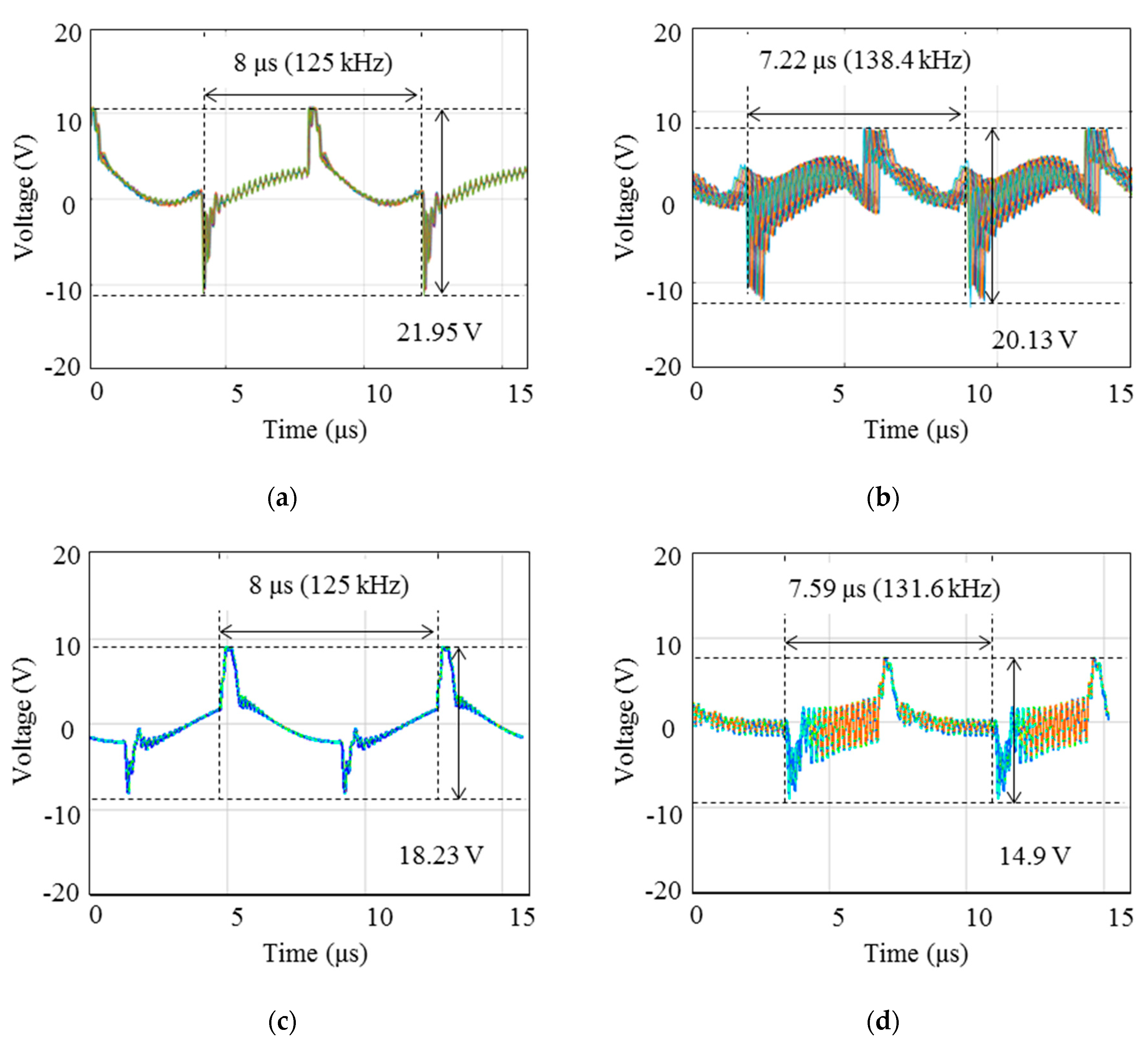
| Transmitted-voltage waveform | Frequency [kHz] | 125 | 138.4 | 125 | 131.6 | 0 | 5.12 |
| Pk-pk voltage [V] | 21.95 | 20.13 | 18.23 | 14.9 | 8.29 | 25.98 | |
| Received-voltage waveform | Frequency [kHz] | 125 | 138.4 | 125 | 131.6 | 0 | 5.12 |
| Pk-pk voltage [V] | 9.83 | 8.24 | 10.1 | 8.91 | 2.74 | 8.13 | |
| DC output | Amplitdue [V] | 4.28 | 4.16 | 4.63 | 4.35 | 8.17 | 4.57 |
| DC Output | With Noise | With Filter 1 | With Filter 2 | With Filter 3 | |
|---|---|---|---|---|---|
| Amplitude (V) | Measurement | 4.16 | 4.17 | 4.2 | 4.22 |
| Simulation | 4.35 | 4.47 | 4.48 | 4.51 | |
| Received-Voltage Waveform | Pk–Pk Voltage (V) | Frequency (kHz) | |
|---|---|---|---|
| Without noise | Measurement | 9.86 | 125 |
| Simulation | 10.1 | 125 | |
| With noise | Measurement | 8.24 | 138.4 |
| Simulation | 8.91 | 131.6 | |
| With noise (filter 1) | Measurement | 8.46 | 138 |
| Simulation | 9.1 | 130.4 | |
| With noise (filter 2) | Measurement | 8.78 | 131.5 |
| Simulation | 9.51 | 129.8 | |
| With noise (filter 3) | Measurement | 9.51 | 128.2 |
| Simulation | 9.71 | 128.2 | |
© 2019 by the authors. Licensee MDPI, Basel, Switzerland. This article is an open access article distributed under the terms and conditions of the Creative Commons Attribution (CC BY) license (http://creativecommons.org/licenses/by/4.0/).
Share and Cite
Joo, J.; Kwak, S.I.; Kwon, J.H.; Song, E. Simulation-Based System-Level Conducted Susceptibility Testing Method and Application to the Evaluation of Conducted-Noise Filters. Electronics 2019, 8, 908. https://0-doi-org.brum.beds.ac.uk/10.3390/electronics8080908
Joo J, Kwak SI, Kwon JH, Song E. Simulation-Based System-Level Conducted Susceptibility Testing Method and Application to the Evaluation of Conducted-Noise Filters. Electronics. 2019; 8(8):908. https://0-doi-org.brum.beds.ac.uk/10.3390/electronics8080908
Chicago/Turabian StyleJoo, Junho, Sang Il Kwak, Jong Hwa Kwon, and Eakhwan Song. 2019. "Simulation-Based System-Level Conducted Susceptibility Testing Method and Application to the Evaluation of Conducted-Noise Filters" Electronics 8, no. 8: 908. https://0-doi-org.brum.beds.ac.uk/10.3390/electronics8080908