Article

An Improved All-Digital Background Calibration Technique for Channel Mismatches in High Speed Time-Interleaved Analog-to-Digital Converters

1
Faculty of Radio-Electronic Engineering, Le Quy Don Technical University, 236 Hoang Quoc Viet Str., Hanoi 100000, Vietnam
2
Graduate School of Informatics and Engineering, The University of Electro-Communications, Chofu-shi, Tokyo 182-8585, Japan
*
Author to whom correspondence should be addressed.
Submission received: 27 November 2019 / Revised: 24 December 2019 / Accepted: 28 December 2019 / Published: 1 January 2020
(This article belongs to the Section Circuit and Signal Processing)

Abstract

:
The time-interleaved analog-to-digital converters (TIADCs), performance is seriously affected by channel mismatches, especially for the applications in the next-generation communication systems. This work presents an improved all-digital background calibration technique for TIADCs by combining the Hadamard transform for calibrating gain and timing mismatches and averaging for offset mismatch cancellation. The numerical simulation results show that the proposed calibration technique completely suppresses the spurious images due to the channel mismatches at the output spectrum, which increases the spurious-free dynamic range (SFDR) and signal-to-noise and distortion ratio (SNDR) by 74 dB and 43.7 dB, respectively. Furthermore, the hardware co-simulation on the field programmable gate array (FPGA) platform is performed to confirm the effectiveness of the proposed calibration technique. The simulation and experimental results clarify the improvement of the proposed calibration technique in the TIADC’s performance.

1. Introduction

With the remarkable growth of next-generation radio communication systems and the development of the new communication standards, the analog-to-digital converters (ADCs) become the essential components. They are responsible for converting the analog signal from the antenna and the high frequency processing unit to the digital signal processing unit. Thus, they are required to be high speed, high resolution, and energy efficient [1,2,3]. Using time-interleaved ADCs (TIADCs) is a promising solution to fulfill these goals [2,3,4,5]. It was first introduced by W. C.Black and D. A. Hodges in [3]. TIADC uses M sub-ADCs that have a low sampling frequency to sample the analog input signal in the time-interleaving mechanism, as depicted in Figure 1. The digital output of each ADC is then multiplexed together to get the overall digital output of TIADC. Theoretically, TIADC’s sampling rate increases to M times the speed of single ADC (where M is the number of single ADCs used for time-interleaving). However, the channel mismatches between sub-ADCs (offset, gain, and timing mismatches) severely decrease the performance of TIADCs [5,6]. Thus, an effective channel mismatch compensation technique is required to eliminate these channel mismatches in order to further boost the system performance.
There are many works coping with the channel mismatches in TIADCs. Some of these perform the channel mismatch calibration in either the all-analog domain or mixed-signal domain [7,8,9,10,11,12]. The all-analog calibration techniques have the drawbacks of very complicated analog estimation circuits, low accuracy, and CMOS technology unsuitability [13]. On the other hand, the mixed-signal calibration techniques require low power consumption and small chip area. However, the correction accuracy is low, and the mixed-signal calibration techniques require some additional analog circuits [14].
Taking the advantages of CMOS scaling and portability between technology nodes, all-digital calibration techniques eliminate the above analog and mixed-signal issues [13,14,15,16,17,18,19,20,21,22,23,24,25,26,27,28,29,30,31]. These techniques often focus on one or two types of mismatches among the gain and timing mismatches, without the offset mismatch [13,14,15,16,17,18,19,20,21,22,23,24,25]. The authors in [30] proposed a technique to calibrate all of three above mismatches. However, the main limitation of this technique is that there is an overlap between the basic function and desired signal when the input signal is single tone spaced at k π / M .
S. R. Khan et al. [31] proposed a method to compensate all offset, gain, and timing mismatches by combining a statistical model for offset calibration, the reference channel for gain compensation, and a derivative filter together with a fractional delay filter for timing skew elimination. However, the TIADC performance in [31] needed to be further improved. In our recent work [32], a calibration technique was proposed for all offset, gain, and timing mismatches with preliminary results without detail analysis, hardware validation, and state-of-the-art comparison. Moreover, in [33], channel deviations were corrected by a similar approach. However, the gain mismatch was calibrated by computing the power ratio between each sub-ADC and the first ADC. Hence, the calibration efficiency needed to be improved, and the hardware validation was not carried out.
Therefore, this work develops an improved all-digital background calibration technique for all offset, gain, and timing mismatches with field programmable gate array (FPGA) hardware validation to further enhance the calibration efficiency in TIADCs and provide a solution for designing high speed ADCs in emerging applications. In the proposed calibration technique, firstly, the offset deviation is calibrated by taking the average of sub-ADC outputs. Next, the gain and timing errors are calibrated by combining a Hadamard transform block and a bandpass derivative filter. Instead of using the ideal differential filter as in [16,32], this work proposes to use a bandpass derivative filter to improve the TIADC performance. This filter allows the proposed TIADC to be applied directly in the next generation direct sampling receivers such as software defined radios, broadband satellite receivers, and sub-sampling receivers. In these receivers, the TIADC can sample the band limited signals in the higher Nyquist band (NB). Moreover, by optimizing the adaptation step of the least mean squares (LMS) algorithm, the proposed calibration method can achieve higher performance and convergence speed compared with the previous techniques. The proposed calibration technique is also validated with an FPGA hardware platform.
The rest of this paper is organized as follows. Section 2 presents the proposed fully digital background calibration technique. Simulation and experimental results on FPGA hardware are analyzed and discussed in Section 3. Finally, Section 4 concludes the paper.

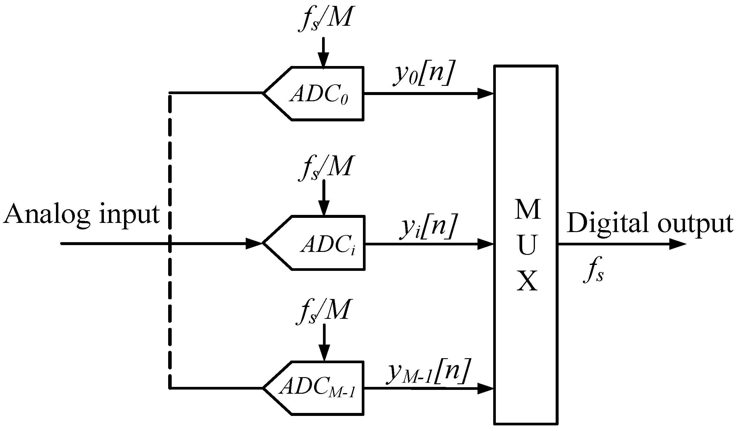
2. Proposed Fully Digital Background Calibration Technique

Consider that the M-channel TIADC model only includes offset mismatch o i , gain mismatch g i , and timing mismatch t i , as shown in Figure 2. With the band limited input and by ignoring the effect of numerical quantization, the i th channel sub-ADC digital output can be written as:
y i k = 1 + g i x k M + i T s + t i + o i
These outputs are then multiplexed together to produce the overall digital output of TIADC as follows:
y t = i = 0 M 1 k = + 1 + g i x t + t i + o i δ ( t ( k M + i ) T )
The proposed calibration technique includes two sequential steps to cope with all three above mentioned mismatches. The first step performs the offset calibration, and the second step calibrates gain and timing mismatches. The proposed calibration technique is illustrated in Figure 3, where F is the M-order Hadamard matrix with the omitted first row.
Firstly, for the offset calibration, let o ^ i be the estimated value of the offset o i for the i th sub-ADC. To calibrate the offset mismatch, the offset o i of the each individual ADC channel needs to be estimated. With the assumption of the wide sense stationary (WSS) input signal, the expected value of the input signal is zero, i.e., 1 N k = 0 N 1 1 + g i x k M + i T s + t i 0 . By averaging the output of each sub-ADC over N samples, the estimated offset of the i th sub-ADC is given as:
o ^ i = 1 N k = 0 N 1 y i k = 1 N k = 0 N 1 1 + g i x k M + i T s + t i 0 + o i o i
Once the estimated offset is known, the offset error can be subtracted from the output of each individual ADC to generate the corrected signal as displayed in Figure 3.
Moreover, for gain and timing mismatches’ calibration, the two steps of mismatch correction and estimation are required. The TIADC output after offset mismatch calibration is expressed by:
y i k = 1 + g i x k M + i T s + t i
As presented in [16,32], the pseudo aliasing signal and its derivative are written as:
x e n = F y n x e n = F y n h d n
where x e [ n ] and x e [ n ] are pseudo aliasing signal vectors caused by gain and timing mismatches, respectively; y [ n ] is the TIADC output. Conventional methods [16,21] used the ideal derivative filter to determine the derivative of the WSS band limited signal at the first NB. The impulse response of the derivative filter ( h d [ n ] ) is expressed as:
h d n = 0 cos ( n π ) n ( n = 0 ) ( n 0 )
Since the ideal derivative filter is effective for the input signal located inside the first NB only, it is not suitable for applications requiring higher NB sampling, i.e., software defined radios, broadband satellite receivers, and sub-sampling receivers. Hence, this work proposes to use another differentiator filter to calculate the derivative of the TIADC output. This filter can work with the input signal at any NB. It is called the bandpass derivative filter, as shown in Figure 4. It consists of a scaling factor dependent on the NB order ( k N B ) and two constant coefficient finite impulse response (FIR) filters including an FIR Hilbert filter h h [ n ] and an ideal differentiator h d [ n ] . The impulse response of Hilbert filter can be expressed as:
h h n = 0 2 π sin 2 ( n π 2 ) n ( n = 0 ) ( n 0 )
With a continuous-time WSS bandpass input signal inside the k N B th , its two frequency components must fulfill Shannon sampling conditions as follows:
k N B 1 f s 2 < f L f f H < k N B f s 2 , k N B 1
where f L and f H are the lowest and highest frequencies of the input bandwidth, respectively.
To avoid aliasing, the condition (8) must be satisfied. Therefore, the proposed structure uses the Hilbert filter to rotate the signal phase by 90 degrees.
The impulse response of the bandpass derivative filter is expressed by:
h b d [ n ] = h d [ n ] + h h [ n ] × ( 1 ) k N B k N B 2 2 π
By substituting h d [ n ] by h b d [ n ] , Equation (5) is rewritten as:
x e n = F y n x e n = F y n h b d n
The corrected signal can be calculated as:
y ^ n = y n c g x e n c t x e n
in which c g and c t are the coefficient vectors, which can be calculated as:
c g 1 M Fg , c t 1 M Ft
where g and t are mismatch vectors that contain values g i and t i , respectively. It is noted that the gain and timing errors are defined as the differences from the average, and the total mismatch of each channel is approximately equal to zero. Therefore, for M-channel TIADCs, it is necessary to reconstruct ( M 1 ) pseudo aliasing signals that cause the gain error and clock skew, respectively. These signals are multiplied by the mismatch coefficient vector and then subtracted from the nonlinear output of TIADC to generate the reconstructed output signal y ^ [ n ] in (11) and as shown in Figure 3. Obviously, the gain and timing mismatch coefficients, expressed in (12), are determined by the proposed estimation technique presented in the next part.
The proposed estimation technique is illustrated in Figure 3. It uses only a bandpass derivative filter as described in Figure 4 and the Hadamard matrix to create the pseudo aliasing signal vector y ^ e n and its derived signal vector y ^ e n . These signal vectors are then correlated with the output of the notch filter. The notch filter is used to eliminate the estimation error y ^ n at k π / M . Since the offset mismatch is removed in the previous step, the correlator works correctly. The proposed estimation technique uses the least mean squares (LMS) algorithm to define the coefficients of (12) as follows:
c ^ g n = c ^ g n 1 + μ g y ^ n y ^ e n
c ^ t n = c ^ t n 1 + μ t y ^ n y ^ e n
where μ g and μ t are the adaptation step sizes for c ^ g and c ^ t , respectively.

3. Results and Discussion

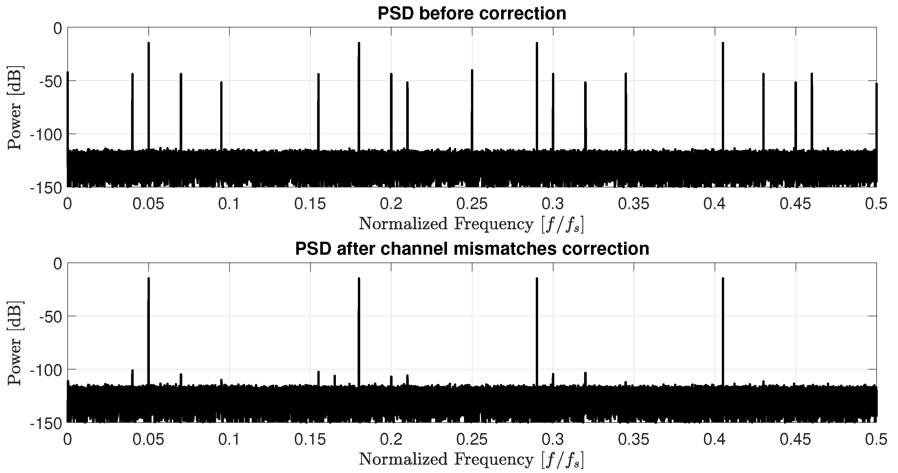
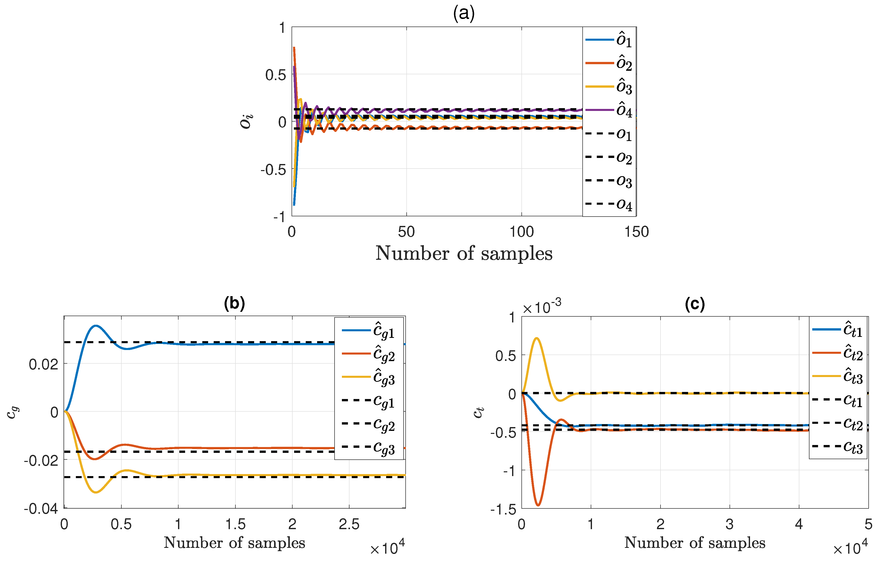
3.1. Simulation Results

To demonstrate the efficiency of the proposed calibration technique, a four channel, 60 dB SNR TIADC clocked at f s = 2.7 GHz with offset, gain, and timing mismatches as presented in Figure 3 was modeled and simulated in MATLAB software. The standard deviations of offset δ o , gain δ g , and timing δ t were 0.07, 0.05, and 0.33 ps, respectively [14]. A 33 tap fixed FIR filter was utilized in the simulations to make the derivative function for both the correction and estimation blocks. To reduce the truncation error, the coefficients of the bandpass derivative filter were determined by multiplying the exact coefficients by the Hanning window. The adaptive steps ( μ g and μ t ) of the LMS algorithm were 2 10 and 2 11 , respectively. A single tone sinusoidal signal with f i n = 0.45 f s was used as an analog input signal.
The simulation results in Figure 5 show that by using the proposed correction technique, the spurs in the output spectrum of TIADC due to three types of channel mismatches were mitigated completely. The TIADC performance was improved significantly. The SNDR after calibration was 59.6 dB, resulting in an improvement of 43.7 dB over the uncompensated output (15.9 dB). Similarly, with the spurious-free dynamic range (SFDR) after calibration being 92.2 dB, an improvement of 74 dB over the uncompensated output (18.2 dB) was achieved.
The TIADC output spectrum for multi-tone sinusoidal input signal before and after calibration for three types of channel mismatches is shown in Figure 6. The fundamental frequencies were 135 MHz, 486 MHz, 780 MHz, and 1094 MHz, respectively. As shown in this figure, the spurs were mitigated completely by employing the proposed technique.
The convergence behavior of the estimated offset, gain, and timing mismatch coefficients is shown in Figure 7a–c, respectively. As can be seen, the estimated offset o ^ i converged very fast, only after 50 samples. The estimated gain c ^ g and timing c ^ t coefficients converged after about 10,000 and 9000 samples, respectively. The calibration efficiency depended on the simulated variables such as channel mismatches, the input frequency, and the number of channels.

3.2. Hardware Implementation and Validation

To confirm the effectiveness of the proposed technique, the hardware validation for the calibration method on the FPGA platform was carried out. The FPGA implementation was to validate that the proposed calibration method could be implemented in hardware. The FPGA design and verification flow using hardware co-simulation with MATLAB/Simulink and Xilinx FPGA design tools were utilized in this framework so that a VHDL (Very High Speed Integrated Circuit Hardware Description Language) model of the TIADC was generated from the MATLAB/Simulink model. The hardware architecture of the proposed calibration technique was designed and optimized in terms of fixed point representation characterized by the signal ranges and signal word length optimized by the design tools.
The hardware based verification flow for the proposed technique with the System Generator tool in MATLAB simulation and the Xilinx FPGA in-the-loop (FIL) methodology is shown in Figure 8. With the TIADC output generated by the computer, both the conventional simulation by MATLAB and the hardware co-simulation with the FPGA board using the FIL methodology were performed. The TIADC output signal included all deviations as described in Section 1 generated by MATLAB 2019a software on the computer. These signals were then loaded into the FPGA board that had the proposed calibration technique embedded through the JTAG USB cable. The results after hardware execution were fed back into the computer for comparison with the simulation results in MATLAB/Simulink. The results included SNDR, SFDR, the output spectrum, and the convergence time. Figure 9 shows the experimental setup for our FPGA implementation consisting of the Xilinx ZYNQ-7000 SoC ZC702 evaluation board, JTAG USB cable, and PC using the FIL method and Xilinx Vivado HL System Edition 2019.1 tool. Figure 9a is the block diagram for the experiments. Figure 9b illustrates the settings and experimental results of the proposed technique in our laboratory.
The experimental results on the FPGA based hardware implementation of the proposed method are shown in Figure 10. The simulation results in Figure 5 and the experimental results in Figure 10 showed good agreement. The performance of TIADC before and after calibration on FPGA hardware implementation was also achieved close to the simulation results. Due to the difference between fixed point and floating point representations, there was still a slight bias in the experimental results.
The convergence behavior of the estimated offset, gain, and timing mismatch coefficients on FPGA hardware is shown in Figure 11a–c, respectively. As can be seen, the estimated offset o ^ i converged very fast, only after 50 samples. The estimated gain c ^ g and timing c ^ t coefficients converged after about 8000 and 9000 samples, respectively. These results were identical to the simulation ones, which again showed the good agreement between the MATLAB simulation and the FPGA hardware experimental results of the proposed technique.
More importantly, the FPGA hardware implementation results confirmed that the synthesized circuit operated properly and consumed small hardware resources of the FPGA chip, as shown in Table 1. Moreover, Table 2 presents the key performance comparison of the proposed calibration with state-of-the-art techniques. It was clear that the proposed calibration technique achieved better performance in terms of the convergence speed, SFDR, and SNDR compared with the previous works. In Table 1, the maximum clock frequency of 102.7 MHz was achieved for the FPGA implementation due to the technology limitation of the XC7Z020 device. For future work, this proposed calibration method will be implemented with an application specific integrated circuit (ASIC) library to obtain better results.

4. Conclusions

An improved all-digital background calibration technique to calibrate all offset, gain, and timing mismatches for TIADCs was presented. In this work, the offset mismatch was corrected by averaging the output samples of each sub-ADC. The gain mismatch and timing skew were compensated by employing the Hadamard transform and a bandpass derivative filter to reconstruct the error signal that was caused by these mismatches. The estimated error signal was subtracted from the output of TIADC to create the corrected one. Simulation and experimental results on FPGA hardware clarified the improvement of the proposed technique in terms of SNDR, SFDR, and convergence time with a little hardware overhead. In our future work, the bandwidth mismatch will be considered to further improve the TIADC performance. Moreover, the fixed point presentational optimization, ASIC synthesis, and chip fabrication for the all-digital background calibration method will be carried out so that it can be applied for next-generation direct sampling receivers.

Author Contributions

Conceptualization, V.-T.T. and V.-P.H.; methodology, investigation, and simulation, V.-T.T.; hardware implementation, V.-P.H., V.-P.P., and C.-K.P.; writing, original draft preparation, V.-T.T.; writing, review and editing, V.-P.H., V.-P.P., and C.-K.P. All authors have read and agreed to the published version of the manuscript.

Funding

This research is funded by Vietnam National Foundation for Science and Technology Development (NAFOSTED) under grant number 102.02-2016.12.

Conflicts of Interest

The authors declare no conflict of interest.

References

  1. Melamed, I.; Toledo, S. A robust, selective, and flexible RF front-end for wideband sampling receivers. ICT Express 2017, 3, 96–100. [Google Scholar] [CrossRef]
  2. Maloberti, F. High-speed data converters for communication systems. IEEE Circuits Syst. Mag. 2001, 1, 26–36. [Google Scholar] [CrossRef]
  3. Black, W.C.; Hodges, D.A. Time interleaved converter arrays. In Proceedings of the 1980 IEEE International Solid-State Circuits Conference, Digest of Technical Papers, San Francisco, CA, USA, 13–15 February 1980; Volume 23, pp. 14–15. [Google Scholar]
  4. Kurosawa, N.; Kobayashi, H.; Maruyama, K.; Sugawara, H.; Kobayashi, K. Explicit analysis of channel mismatch effects in time-interleaved ADC systems. IEEE Trans. Circuits Syst. I Fundam. Theory Appl. 2001, 48, 261–271. [Google Scholar] [CrossRef]
  5. Razavi, B. Design Considerations for Interleaved ADCs. IEEE J. Solid-State Circuits 2013, 48, 1806–1817. [Google Scholar] [CrossRef] [Green Version]
  6. Li, J.; Pan, J.; Zhang, Y. Automatic Calibration Method of Channel Mismatches for Wideband TI-ADC System. Electronics 2019, 8, 56. [Google Scholar] [CrossRef] [Green Version]
  7. Stepanovic, D.; Nikolic, B. A 2.8 GS/s 44.6 mW time-interleaved ADC achieving 50.9 dB SNDR and 3 dB effective resolution bandwidth of 1.5 GHz in 65 nm CMOS. IEEE J. Solid-State Circuits 2013, 48, 971–982. [Google Scholar] [CrossRef]
  8. El-Chammas, M.; Murmann, B. A 12-GS/s 81-mW 5-bit time-interleaved flash ADC with background timing skew calibration. IEEE J. Solid-State Circuits 2011, 46, 838–847. [Google Scholar] [CrossRef]
  9. Doris, K.; Janssen, E.; Nani, C.; Zanikopoulos, A.; Van der Weide, G. A 480mW 2.6GS/s 10b 65nm CMOS time-interleaved ADC with 48.5 dB SNDR up to Nyquist. In Proceedings of the 2011 IEEE International Solid-State Circuits Conference, San Francisco, CA, USA, 20–24 February 2011; pp. 180–182. [Google Scholar]
  10. Camarero, D.; Kalaia, K.B.; Naviner, J.F.; Loumeau, P. Mixed-signal clock-skew calibration technique for time-interleaved ADCs. IEEE Trans. Circuits Syst. I 2008, 55, 3676–3687. [Google Scholar] [CrossRef]
  11. Haftbaradaran, A.; Martin, K.W. A sample-time error compensation technique for time-interleaved ADC systems. In Proceedings of the 2007 IEEE Custom Integrated Circuits Conference, San Jose, CA, USA, 16–19 September 2007; pp. 341–344. [Google Scholar]
  12. Straayer, M.; Bales, J.; Birdsall, D.; Daly, D.; Elliott, P.; Foley, B.; Mason, R.; Singh, V.; Wang, X. 27.5 A 4GS/s time-interleaved RF ADC in 65nm CMOS with 4GHz input bandwidth. In Proceedings of the 2016 IEEE International Solid-State Circuits Conference, San Francisco, CA, USA, 1 January–4 February 2016; pp. 464–465. [Google Scholar]
  13. Le Duc, H.; Nguyen, D.M.; Jabbour, C.; Graba, T.; Desgreys, P.; Jamin, O. All-digital calibration of timing skews for TIADCs using the polyphase decomposition. IEEE Trans. Circuits Syst. II Express Briefs 2016, 63, 99–103. [Google Scholar] [CrossRef]
  14. Le Duc, H.; Nguyen, D.M.; Jabbour, C.; Graba, T.; Desgreys, P.; Jamin, O. Hardware implementation of all digital calibration for undersampling TIADCs. In Proceedings of the IEEE International Symposium on Circuits and Systems, Lisbon, Portugal, 24–27 May 2015; pp. 2181–2184. [Google Scholar]
  15. Le Dortz, N.; Blanc, J.P.; Simon, T.; Verhaeren, S.; Rouat, E.; Urard, P.; Le Tual, S.; Goguet, D.; Lelandais-Perrault, C.; Benabes, P. 22.5 A 1.62 GS/s time-interleaved SAR ADC with digital background mismatch calibration achieving interleaving spurs below 70dBFS. In Proceedings of the 2014 IEEE International Solid-State Circuits Conference Digest of Technical Papers (ISSCC), San Francisco, CA, USA, 9–13 February 2014; pp. 386–388. [Google Scholar]
  16. Matsuno, J.; Yamaji, T.; Furuta, M.; Itakura, T. All-digital background calibration technique for time-interleaved ADC using pseudo aliasing signal. IEEE Trans. Circuits Syst. I Regul. Pap. 2013, 60, 1113–1121. [Google Scholar] [CrossRef]
  17. Satarzadeh, P.; Levy, B.C.; Hurst, P.J. A parametric polyphase domain approach to blind calibration of timing mismatches for M-channel time-interleaved ADCs. In Proceedings of the 2010 IEEE International Symposium on Circuits and Systems, Paris, France, 30 May–2 June 2010; pp. 4053–4056. [Google Scholar]
  18. Divi, V.; Wornell, G.W. Blind calibration of timing skew in time-interleaved analog-to-digital converters. IEEE J. Sel. Top. Signal Process. 2009, 3, 509–522. [Google Scholar] [CrossRef]
  19. Huang, S.; Levy, B.C. Blind calibration of timing offsets for four-channel time-interleaved ADCs. IEEE Trans. Circuits Syst. I Regul. Pap. 2007, 54, 863–876. [Google Scholar] [CrossRef]
  20. Oshima, T.; Takahashi, T.; Yamawaki, T. LMS calibration of sampling timing for time-interleaved A/D converters. Electron. Lett. 2009, 45, 615–617. [Google Scholar] [CrossRef]
  21. Vogel, C.; Saleem, S.; Mendel, S. Adaptive blind compensation of gain and timing mismatches in M-channel time-interleaved ADCs. In Proceedings of the 15th IEEE International Conference on Electronics, Circuits and Systems, St. Julien’s, Malta, 31 August–3 September 2008; pp. 49–52. [Google Scholar]
  22. Jamal, S.M.; Fu, D.; Singh, M.P.; Hurst, P.J.; Lewis, S.H. Calibration of sample-time error in a two-channel time-interleaved analog-to-digital converter. IEEE Trans. Circuits Syst. I Regul. Pap. 2004, 51, 130–139. [Google Scholar] [CrossRef]
  23. Harris, F.; Chen, X.; Venosa, E.; Palmieri, F.A. Two channel TI-ADC for communication signals. In Proceedings of the 2011 IEEE 12th International Workshop on Signal Processing Advances in Wireless Communications, San Francisco, CA, USA, 26–29 June 2011; pp. 576–580. [Google Scholar]
  24. Le Duc, H.; Jabbour, C.; Desgreys, P.; Jamin, O. A fully digital background calibration of timing skew in undersampling TI-ADC. In Proceedings of the 2014 IEEE 12th International New Circuits and Systems Conference (NEWCAS), Trois-Rivieres, QC, Canada, 22–25 June 2014; pp. 53–56. [Google Scholar]
  25. Bonnetat, A.; Hodé, J.M.; Ferré, G.; Dallet, D. Correlation-based frequency-response mismatch compensation of quad-TIADC using real samples. IEEE Trans. Circuits Syst. II Express Briefs 2015, 62, 746–750. [Google Scholar] [CrossRef]
  26. McNeill, J.A.; David, C.; Coln, M.; Croughwell, R. “Split ADC” Calibration for All-Digital Correction of Time-Interleaved ADC Errors. IEEE Trans. Circuits Syst. II Express Briefs 2009, 56, 344–348. [Google Scholar] [CrossRef]
  27. Jamal, S.M.; Fu, D.; Chang, N.J.; Hurst, P.J.; Lewis, S.H. A 10-b 120-Msample/s time-interleaved analog-to-digital converter with digital background calibration. IEEE J. Solid-State Circuits 2002, 37, 1618–1627. [Google Scholar] [CrossRef]
  28. Centurelli, F.; Monsurrò, P.; Trifiletti, A. Efficient digital background calibration of time-interleaved pipeline analog-to-digital converters. IEEE Trans. Circuits Syst. I Regul. Pap. 2012, 59, 1373–1383. [Google Scholar] [CrossRef]
  29. Benabes, P.; Lelandais-Perrault, C.; Le Dortz, N. Mismatch calibration methods for high-speed time-interleaved ADCs. In Proceedings of the 2014 IEEE 12th International New Circuits and Systems Conference (NEWCAS), Trois-Rivieres, QC, Canada, 22–25 June 2014; pp. 49–52. [Google Scholar]
  30. Qiu, Y.; Liu, Y.J.; Zhou, J.; Zhang, G.; Chen, D.; Du, N. All-Digital Blind Background Calibration Technique for Any Channel Time-Interleaved ADC. IEEE Trans. Circuits Syst. I Regul. Pap. 2018, 65, 2503–2514. [Google Scholar] [CrossRef]
  31. Khan, S.R.; Hashmi, A.A.; Choi, G. A fully digital background calibration technique for M-channel time-interleaved ADCs. Circuits Syst. Signal Process. 2017, 36, 3303–3319. [Google Scholar] [CrossRef]
  32. Ta, V.T.; Thi, Y.H.; Le Duc, H.; Hoang, V.P. Fully Digital Background Calibration Technique for Channel Mismatches in TIADCs. In Proceedings of the 2018 5th NAFOSTED Conference on Information and Computer Science (NICS), Ho Chi Minh City, Vietnam, 23–24 November 2018; pp. 270–275. [Google Scholar]
  33. Ta, V.T.; Hoang, V.P.; Tran, X.N. All-Digital Background Calibration Technique for Offset, Gain and Timing Mismatches in Time-Interleaved ADCs. EAI Endorsed Trans. Ind. Netw. Intell. Syst. 2019, 6. [Google Scholar] [CrossRef]
Figure 1. Model of an M-channel TIADC.
Electronics 09 00073 g001
Figure 2. An M-channel architecture of TIADC with offset, gain, and timing mismatches.
Electronics 09 00073 g002
Figure 3. Proposed scheme for multiple channel mismatches’ calibration.
Electronics 09 00073 g003
Figure 4. Bandpass derivative filter for the proposed calibration technique. FIR, finite impulse response.
Electronics 09 00073 g004
Figure 5. The four channel TIADC output spectrum for the single tone sinusoidal input signal before and after calibration. SNDR, signal-to-noise and distortion ratio; SFDR, spurious-free dynamic range.
Electronics 09 00073 g005
Figure 6. The four channel TIADC output spectrum for the multi-tone sinusoidal input signal before and after calibration.
Electronics 09 00073 g006
Figure 7. Convergence behavior of channel mismatches with the proposed technique: (a) offset, (b) gain, and (c) timing.
Electronics 09 00073 g007
Figure 8. The verification flow for the proposed technique with the system generator tool using MATLAB simulation and FPGA in-the-loop (FIL).
Electronics 09 00073 g008
Figure 9. Experimental setup and laboratory measurement for the FPGA based implementation: (a) Experimental setup model, (b) FPGA based measurement in the laboratory.
Electronics 09 00073 g009
Figure 10. The output spectrum after and before calibration on the FPGA hardware implementation of the proposed technique.
Electronics 09 00073 g010
Figure 11. Convergence behavior of channel mismatches with the proposed technique on the FPGA hardware implementation: (a) offset, (b) gain, and (c) timing.
Electronics 09 00073 g011
Table 1. FPGA implementation results.
DeviceXC7Z020 CLG484-1 SoC
LUT10,600/53,200 (19.92%)
Distributed LUT RAM66/17,400 (0.38%)
Flip-Flop (FFs)7281/106,400 (6.84%)
DSP slices30/220 (13.64%)
Fmax102.7 MHz
Table 2. The comparison results with the state-of-the-art techniques.
Calibration TechniqueTCAS-I2013 [16]TCAS-II 2016 [13]TCAS-I 2018 [30]CSSP2017 [31]This Work
Mismatch typesGain, timingTimingOffset, gain, timingOffset, gain, timingOffset, gain, timing
Blind calibrationYesYesYesYesYes
Background calibrationYesYesYesYesYes
Number of sub-ADC channels84484
Sampling frequency ( f s )2.7 GS/s32 GS/s3.072 GS/s2.7 GS/s
Input frequency0.45 f s Multi-tone0.18 f s 0.1 f s 0.45 f s
Number of bits101191211
Convergence time (samples)60K10K40K11K10K
SNDR improvement (dB)251136.552143.7
SFDR improvement (dB)2843.7274

