Cost-Effective High-Performance Digital Control Method in Series-Series Compensated Wireless Power Transfer System


Department of Electrical and Computer Engineering, Seoul National University, Seoul 08826, Korea
*
Author to whom correspondence should be addressed.
Electronics 2020, 9(11), 1772; https://0-doi-org.brum.beds.ac.uk/10.3390/electronics9111772
Submission received: 11 October 2020
/
Revised: 21 October 2020
/
Accepted: 22 October 2020
/
Published: 26 October 2020
(This article belongs to the Special Issue High Performance Power Converters: Design, Control, Devices and Applications)
Abstract
:This paper proposes a control method for a digital signal processor based series-series (SS) compensated wireless power transfer system. In the control method, load resistance and mutual inductance are identified simultaneously, and output voltage can be estimated by using only the primary side voltage and current without direct feedback from the secondary side circuit. Since this estimation method requires a complex mathematical calculation procedure, a digital signal processor is used in this system. One of the major disadvantages of using a digital controller in this system is a limitation of sampling rates. Therefore, in this paper, several current reconstruction methods with limited sampling rates are investigated and applied. As a result, this controller not only reduces the cost of the system but also shows good estimation performance within the limited digital controller unit resource. The proposed control concept is verified by experimental results with a 48W laboratory prototype.
1. Introduction
The wireless power transfer (WPT) system has been used in a variety of applications such as cellular phones, biomedical devices, home appliances, and electric vehicles [1,2,3,4,5,6]. In these systems, the secondary side circuit (receiver) is physically separated from the primary circuit (transmitter), since it is often attached to mobile devices. This means that there is no direct return path for feedback signals from the secondary side circuit. In order to overcome the inherent problem on these systems, additional communication equipment has been commonly utilized to monitor and regulate output voltage [7]. However, due to the growing demand for miniaturization and cost reduction of receivers, a number of techniques have been studied for monitoring the load conditions and regulating the output voltage without a communication link [8,9,10,11,12,13,14,15,16].
The method in [8] allows eliminating the additional communication link by performing the power and data transmission at the same inductive link. However, this method is not suitable for low-power applications due to additional losses in the inductive link. In [9], the load resistance is indirectly identified by using the primary side voltage and current information. Based on the estimation, the output voltage is controlled. Work [10] extends the similar control concept in a system with multiple magnetically coupled coils. However, these studies have only considered the environment of the fixed receiver position for simplicity.
Importantly, WPT applications often demand a flexibility of position of the receiver coil. This implies that the mutual inductance between the primary and secondary side may not be constant. Thus, in order to control the secondary side without any direct measurement, mutual inductance also needs to be estimated. In [11], methods to detect both mutual inductance and load resistance on the secondary side have been presented in SP (series-parallel compensated) topology. In [12,13], methods for the similar purpose with SS (series-series compensated) topology have been proposed. The method in [12] uses a dual-frequency operation; one is for the load resistance estimation, and the other is for the mutual inductance estimation. [13] has shown that the estimation of both parameters is also possible in single frequency operation. However, in both studies, the applicability of a closed-loop voltage control is not evaluated. In [14], the closed-loop control is proposed while estimating the mutual inductance and load resistance in a multi-source and single receiver structure. [15] also presents a primary side closed-loop control method by using a synchronous reference frame model of a series-series compensated inductive power transfer system.
The control methods explained in previous papers require complex mathematical calculation procedures; thus, a digital signal processor (DSP) is usually used. The digital controller updates the control variable at regular intervals to regulate the output voltage. However, one of the major disadvantages of using digital control is a limitation of sampling rates. Especially for a WPT system operating at high frequency, the sampling frequency is not sufficiently higher than the resonance frequency. To solve this problem, an expensive high-end digital controller should be used; otherwise, control performance degradation might follow.
This paper proposes a control method in an SS WPT system in order to overcome the limitation of digital controllers. Based on the previous research [16], further explanation and implementation are described in detail. Including a super-sampling and sub-sampling concept, several current reconstruction methods with limited sampling rates are investigated. In this paper, the primary side control method suitable for SS topology is also presented. The primary side controller monitors both the mutual inductance and the load resistance simultaneously by using the primary side voltage and current. Subsequently, the monitoring parameters are used to estimate the output voltage.
For the experiments, the laboratory prototype is designed to provide a 24V DC-output from a 50V DC-input. The rated power of the prototype is 48W. Experimental results with the prototype are presented to show the validity of the proposed concept.
2. Primary Side Current Reconstruction for Digital Controller
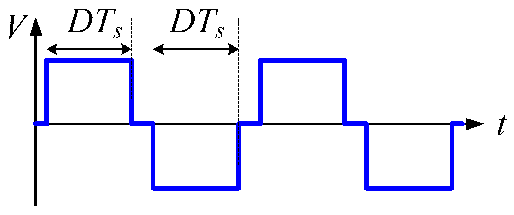
Figure 1 shows the structure of a typical SS compensated WPT system. The phase-shifted full-bridge converter synthesizes the primary side voltage Vp from the dc-input voltage source. The amplitude of the fundamental component of Vp is adjusted by the duty cycle D, while the switching frequency is fixed. Examples of the waveform of Vp determined by D are shown in Figure 2 where Ts is the switching period.
In this paper, the primary side voltage and current are used to estimate and regulate the output voltage instead of using a direct feedback signal from the secondary side circuit. As mentioned, the primary side voltage Vp is directly determined by D, which is the output of the controller; thus, it can be predicted in the digital controller. Therefore, the only component to be measured is the primary side current Ip.
There are several attempts to measure Ip in many previous studies, which have similar purposes. In [13], the external equipment was utilized to measure the current, which makes it difficult to apply to a general WPT system. The methods in [17,18] utilize additional circuits such as an envelop detector and phase detector, together with DSP to extract the required information of the primary side current from the analog signal.
Instead of using additional equipment or circuits, this paper investigates several digital sampling and current reconstruction methods for detecting the amplitude and phase of a current waveform. WPT systems commonly have a high operating frequency comparable to the maximum sampling frequency of DSPs. Therefore, the strategy to reconstruct Ip with limited digital samplings is required. In this paper, the digital sampling methods are categorized by the number of samples per cycle: equal or less than 1 (sub-sampling) and greater than 1 but a limited value (super-sampling). Here, the sampling points can have an equal spacing or non-equal spacing.
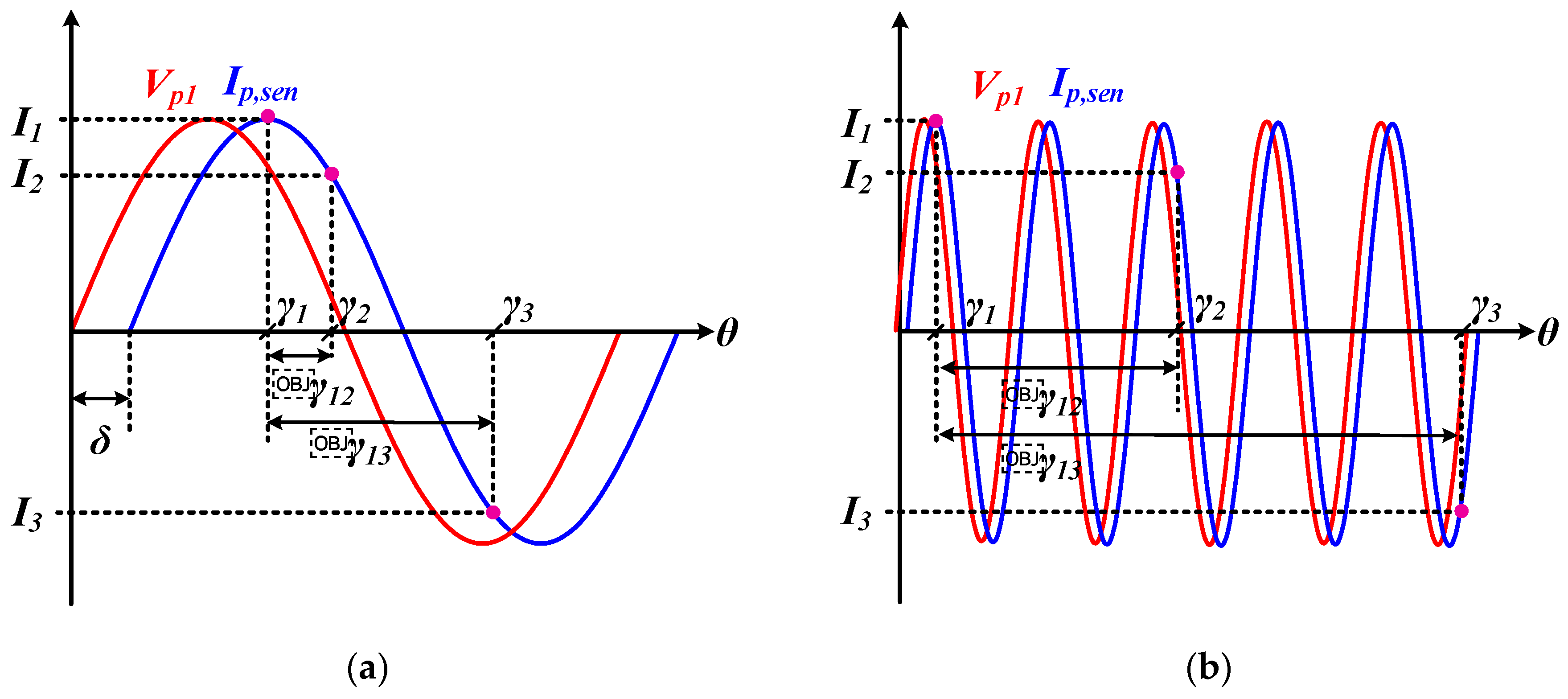
If the current has a sinusoidal waveform under the assumption that a resonator is highly tuned at the resonant frequency and the high-order harmonic components are sufficiently attenuated, the primary side current is represented by:
where Io is an offset of Ip,sen, |Ip| is a magnitude of Ip,sen, θ is the phase angle of the primary side current, and δ is a phase angle difference between Vp1 (the fundamental component of Vp) and Ip.sen. Since the series capacitor connected to the inductor blocks the DC current in SS topology, the offset current is zero in the actual signal. Nevertheless, offset errors occur during the sensing procedure; thus, it is desirable to detect and to compensate the offset current Io.
In order to extract three parameters (Io, |Ip|, and δ) that define the primary side current waveform, at least three independent samples are required. Figure 3a shows the example of the super-sampling case that collects three samples in a cycle. Here, I1, I2, and I3 are the amplitudes of the measured current at θ = γ1, θ = γ2, and θ = γ3 respectively. Then, the sampled values of the primary side current are given as
(2) is rearranged as
where the angle between two points is defined as ∆γ12 = γ2 − γ1 and ∆γ13 = γ3 − γ1. It is noted that the spacing between any two sampling points should not be too close to 180 degrees due to singularity problems. Then, from (3), Io, |Ip|, and δ are calculated as
In a sub-sampling method, the current samples are collected over several cycles, unlike the super-sampling case. Here, the number of samples per cycle, N, is defined as N = y/x where x and y are the number of cycles and the number of samples, respectively. Figure 3b shows the example of sub-sampling where y is 3 and x is 5. This method is useful when the switching frequency is extremely high. In this paper, DSP utilization is defined as the ratio between the algorithm execution time and the control interrupt interval. Table 1 shows the example of DSP utilization according to the switching frequency and sampling methods when the DSP clock is fixed. The DSP utilization should not exceed 100%. Therefore, only the conditions expressed in bold can be implemented in the real system. As shown in the example, the primary side controller is implemented even with a low-cost DSP using the sub-sampling concept. Therefore, this method is also useful for high frequency applications such as a megahertz range power supply.
It is sometimes difficult to assume that the primary side current has a perfect sinusoidal waveform in the real-world situation. For example, since the resonator is usually designed under the rated condition, the waveform of the current may be distorted as the load or the coupling conditions change. The distortion level depends on the specific parameters of the resonator. Even if the harmonic components are removed sufficiently, the current reconstruction using the digital sampling is inevitably sensitive to sensing noise. In these cases, the sub-sampling method with a digital band-pass filter is preferred. By shifting the sampling points slightly at every cycle instead of getting enough samples in one cycle, the controller gets a sufficient number of independent samples for digital band-pass filtering. Figure 4 shows an example of sampling eight points over nine cycles (N = 8/9). The fundamental component of the current waveform can be extracted by using the digital band-pass filter with the collected samples under the assumption that the current waveform changes much slower compared to the sampling frequency. To satisfy this assumption in this paper, the controller holds the switching duty cycle, which is the control variable while collecting all independent samples. Obviously, the more data collected for filtering, the worse the dynamic characteristics of the control. Therefore, the value of N is determined considering the required dynamic performance of the system.
3. Primary Side Control Method
3.1. Output Votlage Estiamation
In the WPT structure shown in Figure 1, the resonator stage consists of loosely coupled coils and compensation capacitors. Lp and Ls are the self-inductances, and Rp and Rs are the resistances of the primary and secondary side coils, respectively. The mutual inductance of the coupled coils is denoted as M. In order to improve the power transfer capability, the capacitors Cp and Cs are connected in series to the coils for compensation. The resonance frequency is determined by
where the parameters for the primary side and secondary side circuit are designed in the same manner. In order to rectify the secondary side voltage denoted as Vs, a passive full-wave rectifier is utilized. The load is represented by the pure resistance RL, and the output voltage to be regulated is denoted by Vo. In the simplified circuit, the rectifier stage is modeled as the equivalent resistance Ro (=8RL/π2) with the assumption that the power is dominantly transferred by the fundamental component and there is no loss in the rectifier circuit. Vs1, which is the voltage across Ro, is the fundamental component of Vs. The amplitude of Vs1 is given by
Since the resonator is usually designed to have a high quality factor at ωo, the system can be simplified to a linear equivalent circuit, as shown in Figure 5, where the system is operated at near ωo. In consideration of the foregoing, the phase-shifted full-bridge converter is modeled as a voltage source having a pure sinusoidal voltage of Vp1 which is the fundamental component of Vp. Here, the amplitude of Vp1 is controlled by the duty cycle D of the converter as
By applying Kirchhoff’s laws in the simplified circuit in Figure 5, the following equations are obtained.
where ω is an operating frequency, Xp = (ωLp − 1/(ωCp)), and Xs = (ωLs − 1/(ωCs)). From (8), the voltage gain G is calculated by
The operating frequency of the system is fixed; thus, Xp and Xs are constant values. Therefore, if the variation in resistance of the coils (Rp and Rs) is neglected, the voltage gain is determined by two parameters: Ro and M. Here, Ro represents the time-varying load power. M is the mutual inductance, which depends on the coil alignment. Since the coil alignment can be freely changed in many applications, M is a variable that is not constant. Therefore, the two parameters Ro and M need to be identified in order to estimate the output voltage Vo.
By analyzing the equivalent circuit in Figure 3, the input impedance Zi is derived as
As shown in (10), the change of Ro and M reflects the change of the input impedance Zi defined as the ratio of Vp1 to Ip. Zi is a complex number that has real and imaginary parts; thus, it is written in polar coordinates as
where |Zi| is a magnitude and ∠Zi is a phase angle of the input impedance Zi. According to (10) and (11), |Zi| and tan(∠Zi) are given by
It is noted that there are two unknown parameters and two equations in Equation (12). It implies that the unknowns can be uniquely identified simultaneously. The value of RL.est and Mest are derived as Equations (13) and (14). Therefore, the output voltage is derived as Equation (15) from Equations (6), (7), (9), (13), and (14).
3.2. Output Votlage Regulation
Figure 6 shows the block diagram of the proposed control method. The proposed control method operates in the following manner. First, the primary side current is reconstructed with one of the digital sampling methods presented in Section 2. Next, the magnitude and phase of Zi are calculated based on the obtained information. They are used for identifying RL and M by Equations (13) and (14), which leads to the output voltage estimation by Equation (15). In order to make the output voltage converge to the desired value, a PI controller is used. The output of the controller is Dref limited to 0 to 1.
4. Experimental Results
4.1. Experimental Setup
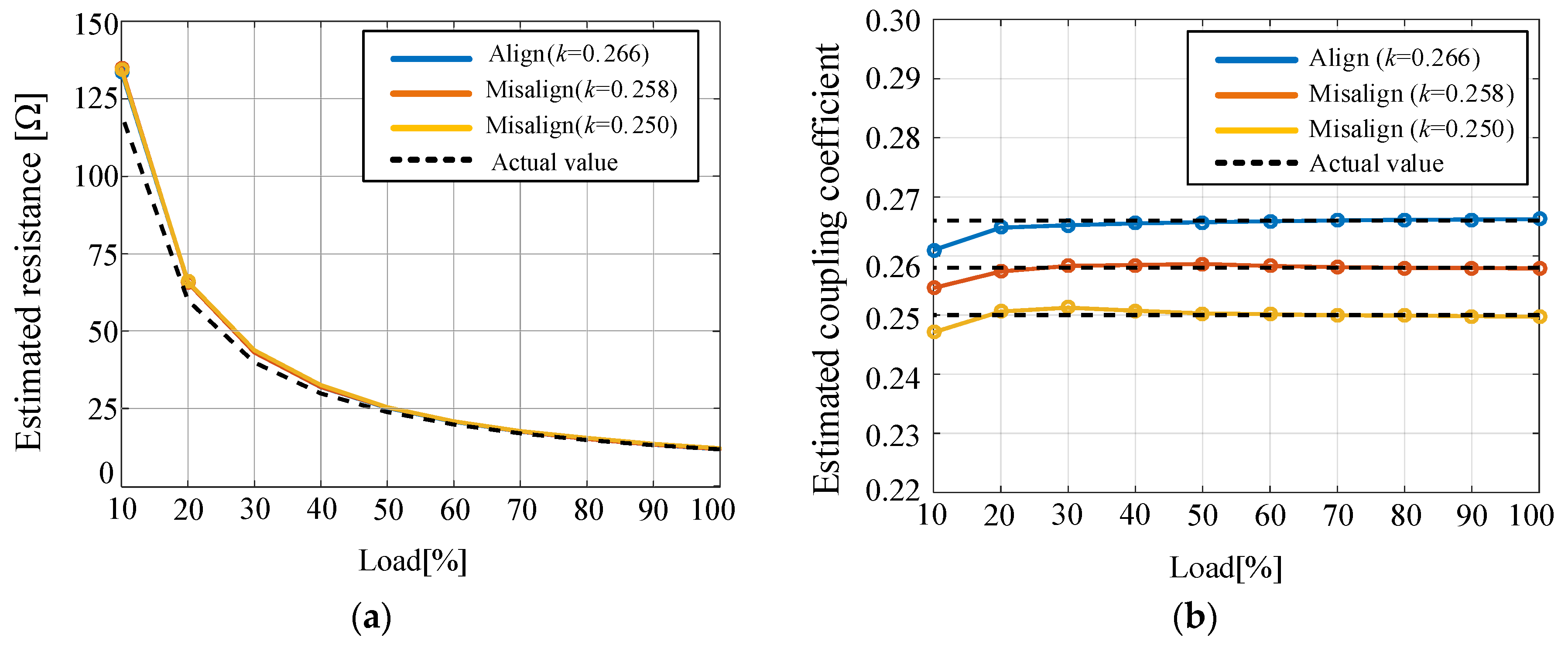
For the experiment, the laboratory prototype is designed to provide 24 V DC-output from 50 V DC-input. The rated power of the prototype is 48 W (RL = 12 Ω). The parameters for the experiment and the detailed information of the resonator setup are listed in Table 2 and Table 3, respectively. The transmitter and the receiver coils are manufactured identically. The distance between two coils is set to 80 mm. The coil system is designed in such a way that their alignment can be manually adjusted. In this section, the coupling coefficient k indicates the alignment of coils instead of M to normalize the value. If the two coils are correctly aligned, k is 0.266(M = 178.0 uH). The value of k decreases to 0.250 (M = 167.5 uH) if the coils are misaligned by 45 mm. The actual value of k is calculated by FEM simulation tool.
The resonance frequency fo is 91.5 kHz. The switching frequency fsw is set to 106.8 kHz to achieve the maximum power transfer at the rated condition. The prototype is regulated by the duty control with the fixed frequency. Here, the range of the duty cycle is limited from 0.3 to 1.0 to account for converter non-linearity such as dead time effects.
In the control board of the prototype, the digital signal processor (TMS320F28377S) is used. As mentioned in Section 2, the current reconstruction using the digital sampling is inevitably sensitive to sensing noises. Therefore, in the below sub-section, the sub-sampling with the digital band-pass filter is applied to verify the proposed control concept. Here, the controller is designed to get 13 independent samples per 14 cycles (N = 13/14). The switching duty cycle, which is the control variable, is updated every 14 cycles to regulate the output voltage. The sampling and control periods can determined differently depending on the system requirements and the performance of digital signal processors.
4.2. Experimental Results
The performance of the estimation procedure is checked before verifying the closed-loop controller. Figure 7 shows the estimated value of (a) RL.est and (b) kest according to the load (10% to 100%, RL = 120 Ω to 12 Ω) and the alignment condition. Here, the actual value is drawn with a dotted line, and the estimated data are drawn with a circular mark connected by a solid line. The blue line represents the case where the coils are correctly aligned (k = 0.266), the orange one represents the case where the coils are misaligned by 4 cm (k = 0.257), and the yellow one represents the case where the coils are misaligned by 4.5 cm (k = 0.250). As shown in Figure 7a, it is noted that RL.est shows almost similar value, regardless of alignment of coils. Moreover, in the case of comparing with real parameters, the estimation error of RL is less than 12% and that of k is less than 2%. The estimation errors in both parameters tend to increase as the load decreases. This is because, as the current signal is decreasing, the estimation process is more susceptible to the current sensing noise, dead time effect, and sampling timing variation due to interrupt latency. The accuracy of the estimation process gets worse at no load or extremely light load condition, since the current level is too low to provide enough information to predict the output voltage. Therefore, the operating range needs to be limited depending on the accuracy of the current measurement and the model parameters.
Figure 8 shows the estimated value of the output voltage calculated from the results of Figure 7. The estimation error of the output voltage is less than 6% for the given load range.
Figure 9, Figure 10 and Figure 11 show the performance of the proposed closed-loop voltage controller. Here, the integral controller is used in the prototype, and the integral gain (Ki) is selected to 40 ensure the stability of the system. Figure 9a,b shows the steady-state waveforms of Vp and Ip at 100% load (RL = 12 Ω) and 20% load (RL = 60 Ω), respectively. As expected, the controller adjusts the switching duty cycle (D) according to load condition in order to control the amount of power delivery and regulate the output voltage.
Figure 10 shows the dynamic performance for the step load change where the two coils are aligned (k = 0.266). Figure 10a shows the waveforms of the switching duty cycle (D), the estimated resistance (RL,est), the estimated coupling coefficient (kest), and the output voltage (Vo) when the step load is applied from 100% to 20%. As shown, the output voltage instantaneously increases due to the step load change. The controller immediately recognizes this voltage change and adjusts D. At the steady state, the output voltage is well regulated to the desired value (24 V) within 6% error. It is noticeable that the estimated value of the load resistance and the coupling coefficient are in good agreement with the actual value. Figure 10b shows the same waveforms of the opposite case in which the load is changed from 20% to 100%. In this case, as well, the output voltage is well regulated at the steady state. In both cases, it takes less than 10 ms to reach the steady state.
Figure 11 shows the experimental transient response when the alignment of the two coils changes. Here, the value of k is varied from 0.266 to 0.250. The experiment is carried out at 100% load condition. Since the rate of change of k is typically much slower than the rate of change of load, the dynamic behavior of the controller is checked, while the alignment of the coils changes over several hundred milliseconds. As shown in Figure 11, when the coil alignment changes, the controller continuously estimates the change of k and the estimation error is kept within 2%. In addition, as expected, the estimated value of the load resistance is consistently maintained within an allowable range regardless of coil alignment. Based on these estimated parameters, the controller estimates and regulates the output voltage.
5. Conclusions
In this paper, a cost-performance digital control method for a series-series compensated wireless power transfer system is proposed. The digital controller can be free from the sampling limitation regardless of resonance frequency thanks to the proposed current reconstruction with sub-sampling. Therefore, the current reconstruction allows high-frequency applications to use a low-cost digital signal processor.
This paper also shows the load estimation method, which uses only the primary side information without any additional circuit. Since the proposed method identifies both parameters resistance and mutual inductance simultaneously, the output voltage can be controlled well, regardless of the load and alignment condition. In the experiments, the load estimation error shows less than 2% at high load and 12% at light load due to low signal-to-noise ratio. Finally, it is verified that the output voltage is regulated with less than 6% error at all conditions.
Author Contributions
Conceptualization, methodology, analysis, and modeling, H.S. and E.C.; experiments, E.C.; writing—original draft preparation, H.S. and E.C.; writing—review and editing the final manuscript, H.S.; recourses and supervision, J.-I.H. All authors have read and agreed to the published version of the manuscript.
Funding
This research received no external funding.
Conflicts of Interest
The authors declare no conflict of interest.
References
- Shinohara, N. Power without wires. IEEE Microw. Mag. 2011, 12, S64–S73. [Google Scholar] [CrossRef]
- Brusamarello, V.J.; Blauth, Y.B.; De Azambuja, R.; Muller, I.; De Sousa, F.R. Power transfer with an inductive link and wireless tuning. IEEE Trans. Instrum. Meas. 2013, 62, 924–931. [Google Scholar] [CrossRef]
- Wang, C.-S.; Covic, G.A.; Stielau, O.H. Power transfer capability and bifurcation phenomena of loosely coupled inductive power transfer systems. IEEE Trans. Ind. Electron. 2004, 51, 148–157. [Google Scholar] [CrossRef]
- Wang, C.-S.; Stielau, O.; Covic, G. Design considerations for a contactless electric vehicle battery charger. IEEE Trans. Ind. Electron. 2005, 52, 1308–1314. [Google Scholar] [CrossRef]
- Sample, A.P.; Meyer, D.T.; Smith, J.R. Analysis, experimental results, and range adaptation of magnetically coupled resonators for wireless power transfer. IEEE Trans. Ind. Electron. 2010, 58, 544–554. [Google Scholar] [CrossRef]
- Ahn, D.; Hong, S. Wireless power transmission with self-regulated output voltage for biomedical implant. IEEE Trans. Ind. Electron. 2013, 61, 2225–2235. [Google Scholar] [CrossRef]
- Miller, J.M.; Onar, O.C.; Chinthavali, M. Primary-side power flow control of wireless power transfer for electric vehicle charging. IEEE J. Emerg. Sel. Top. Power Electron. 2014, 3, 147–162. [Google Scholar] [CrossRef]
- Wu, J.; Zhao, C.; Lin, Z.; Du, J.; Hu, Y.; He, X. Wireless power and data transfer via a common inductive link using frequency division multiplexing. IEEE Trans. Ind. Electron. 2015, 62, 7810–7820. [Google Scholar] [CrossRef] [Green Version]
- Nutwong, S.; Sangswang, A.; Naetiladdanon, S.; Mujjalinvimut, E. Load monitoring and output voltage control for SP topology IPT system using a single-side controller without any output measurement. In Proceedings of the 2016 18th European Conference on Power Electronics and Applications (EPE’16 ECCE Europe), Karlsruhe, Germany, 6–8 September 2016; pp. 1–10. [Google Scholar]
- Yin, J.; Huang, Y.; Lee, C.K.; Hui, S.Y.R. A systematic approach for load monitoring and power control in wireless power transfer systems without any direct output measurement. IEEE Trans. Power Electron. 2014, 30, 1657–1667. [Google Scholar] [CrossRef]
- Chow, J.P.W.; Chung, H.S.H. Use of primary-side information to perform online estimation of the secondary-side information and mutual inductance in wireless inductive link. In Proceedings of the 2015 IEEE Applied Power Electronics Conference and Exposition (APEC), Charlotte, NC, USA, 15–19 March 2015; pp. 2648–2655. [Google Scholar]
- Chung, E.; Lee, J.; Ha, J.-I. System conditions monitoring method for a wireless cellular phone charger. In Proceedings of the 2014 International Power Electronics and Application Conference and Exposition, Shanghai, China, 5–8 November 2014; pp. 639–643. [Google Scholar]
- Yin, J.; Lin, D.; Parisini, T.; Hui, S.Y. Front-end monitoring of the mutual inductance and load resistance in a series–series compensated wireless power transfer system. IEEE Trans. Power Electron. 2015, 31, 7339–7352. [Google Scholar] [CrossRef]
- Wang, C.; Zhu, C.; Song, K.; Wei, G.; Dong, S.; Lu, R.G. Primary-side control method in two-transmitter inductive wireless power transfer systems for dynamic wireless charging applications. In Proceedings of the 2017 IEEE PELS Workshop on Emerging Technologies: Wireless Power Transfer (WoW), Chongqing, China, 21–22 May 2017; pp. 1–6. [Google Scholar]
- Lee, S.; Lee, J.; Noh, E.; Gil, T.; Lee, S.-H. Load estimation of a series-series tuned wireless power transfer system. In Proceedings of the 2019 IEEE Energy Conversion Congress and Exposition (ECCE), Baltimore, MD, USA, 29 September–3 October 2019; pp. 4216–4222. [Google Scholar]
- Chung, E.; Lim, G.C.; Ha, J.-I.; Kim, K.Y. Output voltage control for series-series compensated wireless power transfer system without direct feedback from measurement or communication. In Proceedings of the 2017 IEEE Energy Conversion Congress and Exposition (ECCE), Cincinnati, OH, USA, 1–5 October 2017; pp. 4035–4040. [Google Scholar] [CrossRef]
- Namadmalan, A. Self-oscillating tuning loops for series resonant inductive power transfer systems. IEEE Trans. Power Electron. 2015, 31, 7320–7327. [Google Scholar] [CrossRef]
- Wang, Z.-H.; Li, Y.-P.; Sun, Y.; Tang, C.-S.; Lv, X. Load detection model of voltage-fed inductive power transfer system. IEEE Trans. Power Electron. 2013, 28, 5233–5243. [Google Scholar] [CrossRef]
Figure 1.
Wireless power transfer (WPT) system based on series-series compensated (SS) topology.

Figure 2.
Voltage waveforms synthesized by phase-shifted full-bridge converter according to the switching duty cycle D.
Figure 2.
Voltage waveforms synthesized by phase-shifted full-bridge converter according to the switching duty cycle D.

Figure 3.
Example of sampling points of current waveform of (a) super-sampling, (b) sub-sampling.

Figure 4.
Example of the original signal and sampled points where y = 8 and x = 9 (N = 8/9).

Figure 5.
The equivalent circuit of the simplified WPT system.

Figure 6.
Block diagram of the proposed digital control method.

Figure 7.
The estimated value of (a) RL and (b) k according to load and alignment condition.

Figure 8.
The estimated value of the output voltage according to load and alignment condition.

Figure 9.
Waveforms of the primary side voltage (Vp) and current (Ip) at (a) 100% load (RL = 12 Ω) and (b) 20% load (RL = 60 Ω).
Figure 9.
Waveforms of the primary side voltage (Vp) and current (Ip) at (a) 100% load (RL = 12 Ω) and (b) 20% load (RL = 60 Ω).

Figure 10.
Waveforms of the switching duty cycle (D), estimated resistance (RL,est), estimated coupling coefficient (kest), and output voltage (Vo) where k = 0.266. A step load is applied from (a) 100% to 20% and (b) 20% to 100%.
Figure 10.
Waveforms of the switching duty cycle (D), estimated resistance (RL,est), estimated coupling coefficient (kest), and output voltage (Vo) where k = 0.266. A step load is applied from (a) 100% to 20% and (b) 20% to 100%.

Figure 11.
Waveforms of the switching duty cycle (D), estimated resistance (RL,est), estimated coupling coefficient (kest), and output voltage (Vo), where the coupling coefficient varied from 0.266 to 0.250.
Figure 11.
Waveforms of the switching duty cycle (D), estimated resistance (RL,est), estimated coupling coefficient (kest), and output voltage (Vo), where the coupling coefficient varied from 0.266 to 0.250.


Table 1.
Digital signal processor (DSP) utilization of each sampling method.
| Method fsw | Super-Sampl. (N = 3) | Sub-Sampl. 1 (N = 3/4) | Sub-Sampl. 2 (N = 3/40) |
|---|---|---|---|
| 10 kHz | 32% | 8% | 0.8% |
| 100 kHz | 320% | 80% | 8% |
| 1000 kHz | 3200% | 800% | 80% |
Table 2.
Parameters for experiments.
| Parameters | Value |
|---|---|
| Lp, Ls | 670 [uH] |
| Rp, Rs | 1.6 [Ω] |
| Cp, Cs | 4.52 [nF] |
| fo | 91.5 [kHz] |
| fsw | 106.8 [kHz] |
| Co | 220 [μF] |
Table 3.
Description of resonator setup.
| Coil diameter | 260 [mm] |
| Vertical distance | 80 [mm] |
| Horizontal distance (Align) | 0 [mm] |
| Horizontal distance (Misalign) | 45 [mm] |
| Shielding material | TDK B67410-N95 |
Publisher’s Note: MDPI stays neutral with regard to jurisdictional claims in published maps and institutional affiliations. |
© 2020 by the authors. Licensee MDPI, Basel, Switzerland. This article is an open access article distributed under the terms and conditions of the Creative Commons Attribution (CC BY) license (http://creativecommons.org/licenses/by/4.0/).
Share and Cite
MDPI and ACS Style
Shin, H.; Chung, E.; Ha, J.-I. Cost-Effective High-Performance Digital Control Method in Series-Series Compensated Wireless Power Transfer System. Electronics 2020, 9, 1772. https://0-doi-org.brum.beds.ac.uk/10.3390/electronics9111772
AMA Style
Shin H, Chung E, Ha J-I. Cost-Effective High-Performance Digital Control Method in Series-Series Compensated Wireless Power Transfer System. Electronics. 2020; 9(11):1772. https://0-doi-org.brum.beds.ac.uk/10.3390/electronics9111772
Chicago/Turabian StyleShin, Hojoon, Euihoon Chung, and Jung-Ik Ha. 2020. "Cost-Effective High-Performance Digital Control Method in Series-Series Compensated Wireless Power Transfer System" Electronics 9, no. 11: 1772. https://0-doi-org.brum.beds.ac.uk/10.3390/electronics9111772
Note that from the first issue of 2016, this journal uses article numbers instead of page numbers. See further details here.