Influence of Structural Defects on the Resistivity and Current Flow Field in Conductive Thin Layers


1
Department of Electrodynamics and Electrical Machine Systems, Faculty of Electrical and Computer Engineering, Rzeszow University of Technology, 35-959 Rzeszow, Poland
2
Department of Power Electronics and Power Engineering, Faculty of Electrical and Computer Engineering, Rzeszow University of Technology, 35-959 Rzeszow, Poland
3
Institute of Electrical Engineering Systems, Faculty of Electrical Engineering, Electronics, Computer and Control Engineering, Lodz University of Technology, 90-924 Lodz, Poland
*
Author to whom correspondence should be addressed.
Electronics 2020, 9(12), 2164; https://0-doi-org.brum.beds.ac.uk/10.3390/electronics9122164
Submission received: 17 November 2020
/
Revised: 10 December 2020
/
Accepted: 14 December 2020
/
Published: 17 December 2020
(This article belongs to the Special Issue Electromagnetism in Electronics, Modern Engineering and Medical Applications)
Abstract
:The paper presents an analysis of the influence of microcracks in textronic conductive layers on their conductive properties. The tested structures were created in the physical vacuum deposition process. The paper presents the results of computer simulations of the current flow field in thin conductive stripes with defects distributed along a line perpendicular to the stripe axis and randomly placed on its entire surface. It was found, inter alia, that a larger number of shorter collinear defects may have many times lower resistance than a small number of longer defects of the same total length (e.g., with 40 collinear cracks with a total length of 90% of the strip width, the sheet resistance is only about 3% greater compared to a track without cracks). It was found that the percolation threshold of the tested models with square proportions and randomly selected defects is close to the value of 0.5. This is consistent with the theoretical calculations for analogous discrete models with infinite sizes. It was also found that the sheet resistance of the conductive strip with randomly distributed defects clearly depends on its length when the defect concentration exceeds 20%. The simulations were carried out on the basis of the integral equation method, with the solution presented in the form of double layer potentials.
1. Introduction
Smart textiles and wearable electronics are some of the areas of interest for scientists in the 21st century. In both cases, it is important to create electroconductive elements in the form of thin layers on a flexible substrate or in the entire volume of textiles. For this purpose, various processes for connecting textiles with electrically conductive elements are used. These include embroidery [1], digital printing [2], magnetron sputtering [3,4], chemical vapor deposition (CVD) [5], and electroless deposition [6].
Physical vacuum deposition (PVD) is also one of the methods for producing such structures [7,8,9]. PVD technology makes it possible to replace metallization with chemical processes. It is environmentally friendly and can be used on nonpolar polymeric substrates such as polypropylene and polyethylene. In such a process, a controlled transfer of metal atoms with a low resistivity value from the heated source to the substrate located at a short distance is observed. The metal atoms, as a result of providing them with an appropriate amount of thermal energy, boil and then evaporate. An electroconductive layer is formed and grows atom by atom, ultimately forming a thin pure metal coating that adheres strongly to the substrate. Thermal evaporation differs from sputtering, another method of physical deposition of thin layers; during sputtering, atoms are ejected from the source surface under the influence of gaseous ions [3,4]. Most often, the source is at room temperature. Both technologies were initiated in the second half of the 19th century. In 1852, Grove [10] observed the deposition of metal sputtered from the cathode of the glow discharge plasma. On the other hand, in 1857, Faraday [10], experimenting with exploding fuse-like metal wires in an inert atmosphere, evaporated thin films. The development of material technologies and the possibility of producing appropriate Joule heat sources (first from platinum, then from tungsten), as well as progress in the construction of technical solutions in the field of vacuum devices, accelerated the development of PVD technology.
PVD technology is known primarily in mechanical engineering for the production of durable coatings with high adhesion to the substrate and resistant to corrosion [11]. Using this method of producing thin layers on other substrates, it is also possible to modify the fatigue behavior of metallic surface [11]. Thanks to these properties, their application have been extended to the biomedical field [11]. In this field, it is important to create electroconductive structures on flexible textile substrates [8,9]. Flexibility plays a key role in elements used in wearable electronics. In the process of use, multiple bending occurs, and thus the appearance of numerous microcracks formed in the produced electroconductive layer, leading also to changes in the ampacity of the layers and the appearance of local hotspots due to the local increase of the current density [12,13]. The conductivity of thin layers depends strongly on their morphology and structure. The assessment of the surface of such a structure is possible, for example, by means of tomography [14,15,16,17]. Sheet resistance is one of the parameters that describe the properties of material taking into account the electroconductivity. It results, among other factors, from the morphology of thin films. It can be modified with oxidation [18] or photochemical oxidation [19]. The low sheet resistance could benefit conductor applications, such as those in [20,21,22].
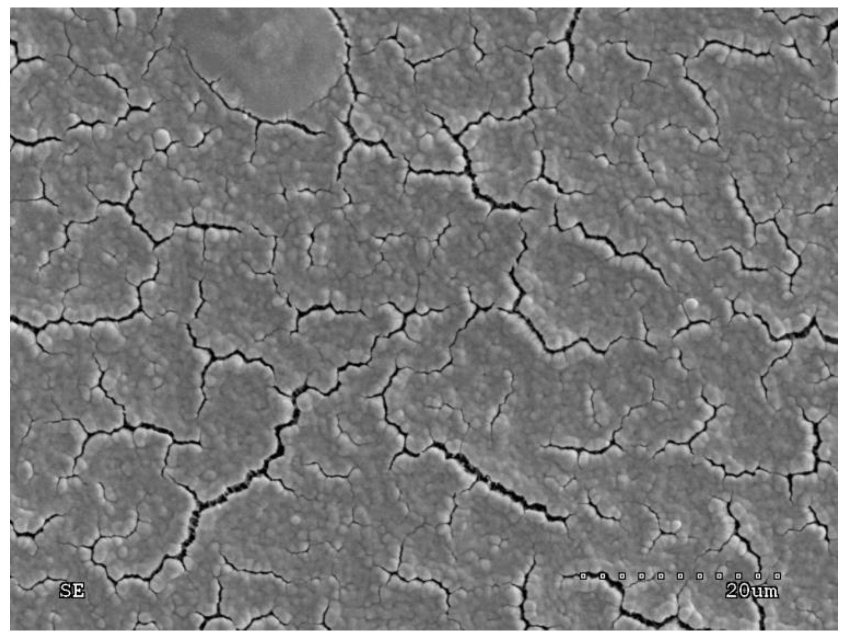
The problem of current flow and the properties of thin conductive layers is an issue studied by various research groups [23,24]. In the literature, it is possible to find research papers on the transport properties of such materials, with most of the results presented in line with the predictions based on the percolation theory [24,25,26,27]. It is known that there is a significant change in the physical properties during the percolative transition from the islet structure to the continuous film and vice versa, due to spatial and dimensional constraints in the thin film [28,29,30,31]. The electrical conductivity of the thin layer also shows a clear transition from two-dimensional to three-dimensional behavior with increasing layer thickness [24]. In the literature, correlations can be also found between the properties of electric conductivity and the porosity of the structure of a thin layer, created by applying vacuum methods [24]. The influence of defects on the current density in the structure produced in the PVD process was also analyzed by the authors of this paper in previous articles [12,13]. In the previous studies, the authors researched the effect on the current flow field and total current in a conductive stripe with one or two defects of a size comparable to the stripe width. Such defects may arise from bending or tensile stresses during the use of the fabric underlying the stripe. Microscopic examination of the conductive layers created in PVD technology shows that there are also other types of defects that occur during the technological process itself, which may also increase during use. These are usually small cracks randomly distributed over the entire surface of the metallic layer (Figure 1). The aim of this research is to study their influence on the conductive properties of the stripe through numerical simulations, which allows us to understand the phenomenon of electrical conductivity in electroconductive thin films produced in the PVD process. The simulations were carried out on the basis of the integral equation method. Due to the specific nature of the boundary conditions on the defect lines (potential discontinuity), double layer potentials were used in the presented case. The compatibility of the theoretical model and the computational method with a physical experiment in the case of single linear defects was already presented in the previous publications [12,13].
2. Description of the Model and Formulation of the Problem
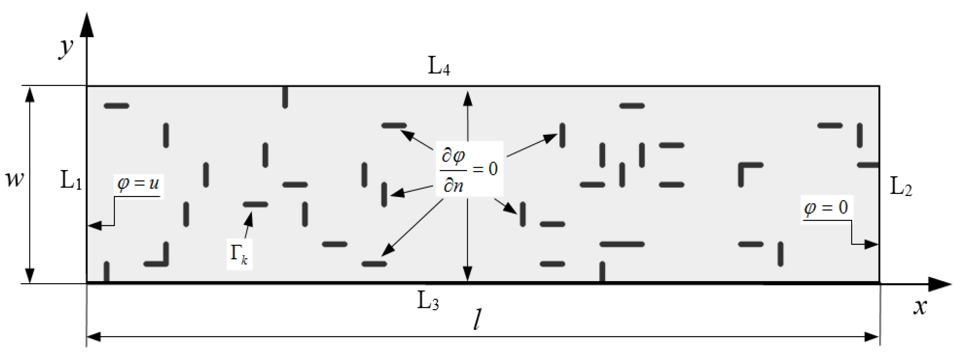
The defects in textronic layers are usually in the shape of scratches (cracks), the widths of which are much smaller than their lengths (see Figure 1). This suggests the possibility of modeling them as infinitely thin, i.e., with lines that constitute a barrier to the flow of current. Such an idealization may, however, raise some doubts due to the peculiarities that appear at the extreme points of the defect line. As it results from the precise analytical solution described in [12,13] for a single defect with the shape of a rectilinear segment, the current density at its ends assumes infinite values (despite the continuity of the potential). It was shown in [32] that this effect can introduce a significant error in the calculation of the total current flowing in the conducting stripe (Figure 2) only when the length of the defect is close to the width of the stripe and when at least one of its ends is at a distance comparable to the width of the defect. In this paper, the impact of defects with lengths much smaller than the stripe sizes is analyzed, and it was concluded that modeling them as infinitely thin does not significantly affect the simulation results.
The subject of the problem is therefore the search for the distribution of the vector field current density J and the total current intensity in a thin conductive layer, rectangular in shape (named here as “stripe”), containing defects in the shape of rectilinear sections. The model geometry is illustrated in Figure 2.
Moreover, the following assumptions were made:
- The area of the conductive stripe is a uniform, isotropic, and linear (with constant electrical conductivity) rectangular conductor.
- The defects and the surroundings of the track are areas of zero electrical conductivity (ideal dielectric).
- A constant voltage u is applied between the ends of the stripe (lines L1 and L2 in Figure 2).
- The field functions do not depend on the coordinate z perpendicular to the surface of the stripe.
- The stationary operating condition of the system is analyzed (field functions do not depend on time).
- There are no unbalanced electric charges in the system.
Under the assumptions made, the electric field E is expressed through the electric potential φ:
which satisfies the Laplace’s equation [33]
The sought function of the current density field J can be related to the electric field strength E by the relationship (local Ohm’s law):
where γ is the conductivity of the layer.
According to Assumptions 4 and 5, we have φ = φ (x, y). The boundary conditions for the potential φ on the side edges of L1 and L2 are given by the dependencies
From Assumptions 2 and 6, it follows that the normal components of the vector J on the edges L3 and L4, as well as on the defect lines, equal to zero, which according to (1) and (3) means that the potential meets the conditions of the Neumann type:
where Γk denotes defect lines (see Figure 2).
Therefore, the problem comes down to the search for a solution to the Laplace Equation in (2) with mixed boundary conditions, i.e., in (4) and (5). In order to solve it, the method of integral equations was used.
The searched potential function is presented in the form
where σm and σk are density potential functions of double layer on Lm and Γk lines, respectively; R is the distance between any point of the analyzed area and the current integration point; and α is the angle between the line connecting these points and normal to the shoreline.
The first part of Equation (6) on the right meets all the conditions of the problem except the boundary condition on the Γk defect lines, and thus it corresponds to the original field.
The second part corresponding to the field induced by the stripe edges and the third part—the field induced by the defects—are represented by the double layer potentials. A detailed description of the numerical determination of the density function of these potentials and the algorithm of the entire field calculation procedure are provided in the previous article [13].
The applied method belongs to the category of boundary methods, which allows for obtaining faster and more accurate algorithms than in the case of commonly used area methods (e.g., the finite element method-FEM). Solution (6) satisfies Equation (2) exactly. The numerical error concerns only the fulfilment of the boundary conditions. This makes it possible to calculate the gradient in (1) without additional error as well as a relatively easy evaluation of the accuracy of the solution.
The numerical application was implemented in a Microsoft Visual Studio 2010 environment in Fortran 77 language. This enables the calculation of the flow field distribution and the current intensity in a stripe containing any number of defects of any given shape.
3. Results
3.1. Collinear Defects
The purpose of these simulations was to investigate how the current in the conductive layer depends on the number of defects on one line, assuming that the total length of these defects is the same in each case. Defect lines were assumed to be perpendicular to the stripe axis and that their lengths are the same. The gaps between defects are also the same. The distribution of the potential and the flow field was analyzed depending on the percentage of the total length of defects ds in relation to the width of the stripe w.
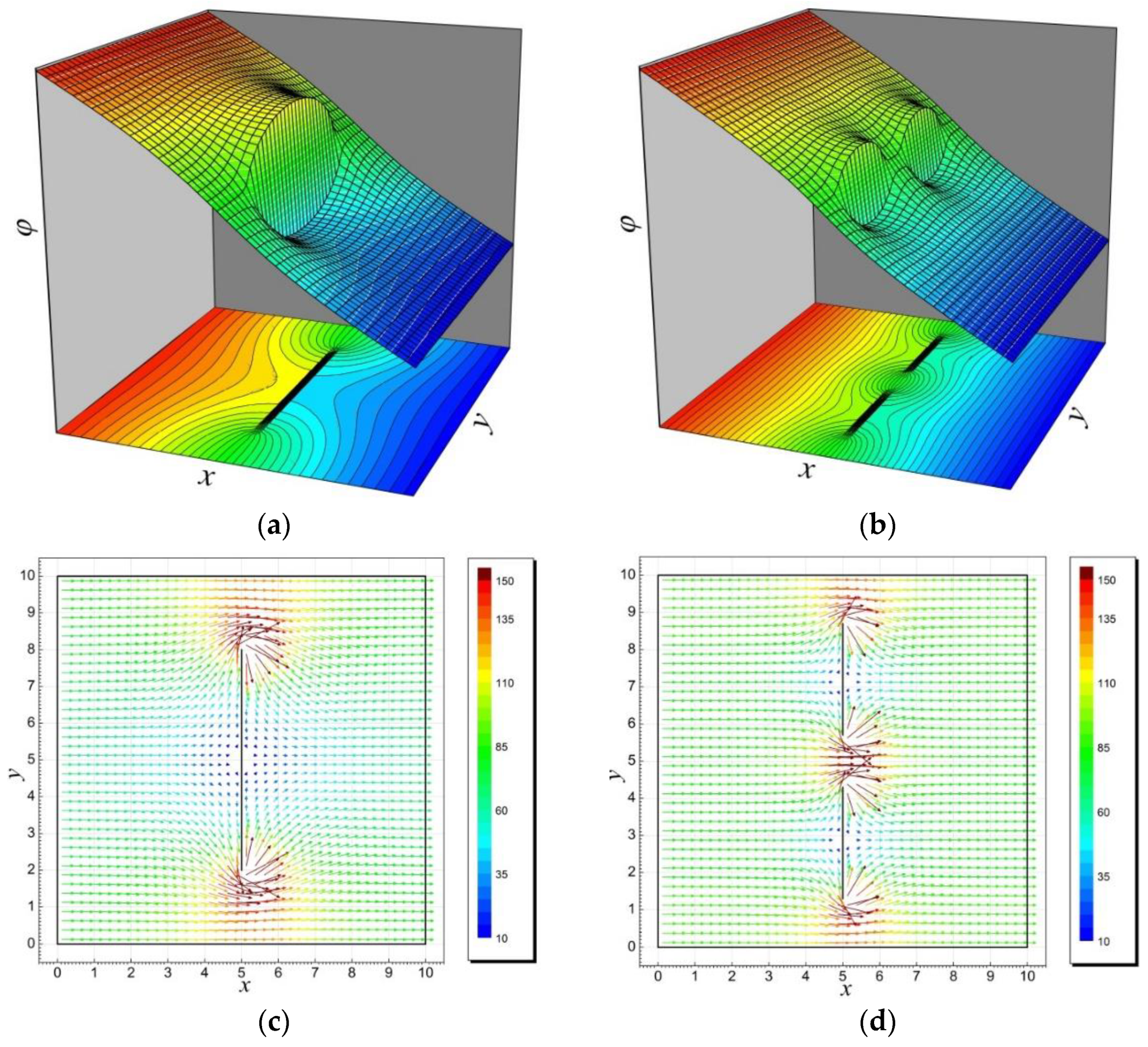
Figure 3 shows examples of the calculation of the potential distribution and the current density flow field for one, two, three, and ten collinear defects with a total length ds = 60% of the whole strip width. The plots created for the potential show a sharp change in their value on the defect line. This effect is confirmed by the analytical calculations presented in [12,13]. When the number of defects increases, these changes decrease to zero, and the dependence of the potential on the x coordinate becomes linear, as for a strip without defects.
The calculated current values in each of these cases indicate that the greater number of short defects has less impact on the current limitation in the stripe than the smaller number of long defects of the same cumulative length. The reasons for this effect can be seen in the fact that near the end points of the defects, the current density reaches the highest values, so that a greater number of such points allows for a greater current value. The results of calculations of the current intensity for the different numbers of cracks Ns and their different total lengths ds are presented in the charts in Figure 4. Particular attention is drawn to the fact that regardless of how large the total length of the cracks is, if their number increases, the current intensity tends to the same value imax, i.e., the value which would appear in a stripe without defects.
It should also be noted that high values of current density in the vicinity of the end points of defects may be the cause of local overheating of the material and, as a result, their increase. Moreover, inside the defects near these points, high values of electric field intensity can be expected, which may cause damaging electric microdischarges.
3.2. Stochastic Defects in a Square Area
The purpose of the simulations was to investigate how randomly distributed defects affect the conductive properties of the stripe. In the adopted model, defects are automatically and stochastically placed (using a pseudorandom number generator) from among the sections of a regular sieve covering the stripe area (Figure 5). The problem formulated in this way is an example of the “bond percolation” problem on a square lattice [34]. Classic solutions to this type of problems are based on discrete models. In this study, the field method [35,36] was used to obtain the values of the current, taking into account the exact image of the flow field.
The first stage of the research consisted of calculating the distribution of the flow field and the current intensity in a square area.
The variable parameters were the mesh size and the number of defects, which are represented by the ratio:
where N is the number of cracks, Nn is the number of all mesh sections, and Nb is the number of mesh sections at the edges of the stripe.
In order to determine how the stochastic nature of the model may affect the value of the current intensity, a series of simulations were carried out for models with the same parameters but with differently distributed defects. The results of these tests are presented in the charts in Figure 6. As it should be expected, the relative standard deviations for the mean current values are larger when the model is smaller (i.e., containing fewer mesh elements), and the greater the ratio p of the number of defects to all mesh sections is. From these charts it can also be concluded that the percolation threshold of the studied models is close to the value of p = 0.5, which corresponds to the theoretical value for an analogous discrete model with infinite sizes determined by H. Kesten [37].
On the basis of the simulations described, the dependencies of the current intensity as a function of p were plotted in Figure 7.
3.3. Stochastic Defects in a Rectangular Area
The lengths of the actual conducting stripes are usually at least several times greater than their widths. With the made assumptions, the dependence of the resistance of the conductive stripe without defects is proportional to its length, but the presence of defects makes the stripe area not homogeneous and this relationship cannot be easily derived from the results for the square area (it is enough to note that near the percolation threshold extending the conductive stripe significantly increases the probability of blocking the current flow completely).
Figure 8 shows the results of the stripe resistivity tests depending on its l/w ratio for different mesh sizes and the number of defects. From them, it can be concluded that the stripe resistivity significantly depends on the stripe length for p ≥ 0.3. At p ≥ 0.4 concentrations and l/w > 4 stripe ratios, defects usually form a structure that prevents the flow of current. The proximity to the percolation threshold in this case makes the strip resistance strongly dependent on the specific defect randomization, which explains the large values of the spread bars in Figure 8.
4. Conclusions
The paper presented the results of a simulation of the current flow field in thin conductive stripes with defects distributed along a line perpendicular to the stripe axis and distributed randomly over its entire surface. Based on the calculations, the following conclusions were drawn:
- The increase in stripe resistance caused by collinear defects (see Figure 3) depends not only on their total length but also on their number. A larger number of shorter defects may present many times less resistance than a small number of longer defects of the same total length (see the plot in Figure 4).
- For a set summary length of infinitely thin collinear defects, the increment of resistance (ΔR) caused by them decreases to zero as their number increases.
- Simulations of the current flow in layers containing many distributed linear defects generated randomly on a square grid (Figure 5) confirm the theoretical value of the percolation threshold for the analogous problem of the discrete model with infinite dimensions at the level of p = 0.5.
- Due to the stochastic nature of the analyzed models, the calculated values of the current intensity may differ significantly, despite the same parameters of these models (Figure 6 and Figure 7). The smaller the model is (fewer mesh elements), the greater the scatter of these values (relative standard deviation) is. Regardless of the size of the model, it is relatively small in the range of 0 ≤ p ≤ 0.2. After exceeding this value, it begins to increase quite rapidly, reaching the highest values near the percolation threshold.
- Averaged current values are similar for models of different sizes in the range of 0 ≤ p ≤ 0.35 (Figure 7). In this range, it can be concluded that the calculations of the conductive layer resistance for relatively small calculation models (e.g., 10 × 10) are, after averaging, adequate for models of any size.
- The sheet resistance of a stripe with defects may increase with its length. This effect becomes visible at p = 0.2, and it becomes clearer when approaching the percolation threshold (Figure 8).
Author Contributions
Conceptualization, S.P. and E.K.; data curation, S.P., J.P. and E.K.; formal analysis, S.P. and J.P.; investigation, S.P., J.P. and E.K.; methodology, S.P., J.P. and E.K.; supervision, S.P. and E.K.; validation, S.P. and J.P.; visualization, S.P., J.P. and E.K.; writing—original draft, S.P., J.P. and E.K.; writing—review and editing, S.P., J.P. and E.K. All authors have read and agreed to the published version of the manuscript.
Funding
This research received no external funding.
Conflicts of Interest
The authors declare no conflict of interest.
References
- Jakubas, A.; Łada-Tondyra, E. A study on application of the ribbing stitch as sensor of respiratory rhythm in smart clothing designed for infants. J. Text. Inst. 2018, 109, 1208–1216. [Google Scholar] [CrossRef]
- Stempien, Z.; Rybicki, E.; Patykowska, A.; Rybicki, T.; Szynkowska, M.I. Shape-programmed inkjet-printed silver electro-conductive layers on textile surfaces. J. Ind. Text. 2018, 47, 1321–1341. [Google Scholar] [CrossRef]
- Miśkiewicz, P.; Tokarska, M.; Frydrych, I.; Makówka, M. Evaluation of Thermal Properties of Certain Flame-Retardant Fabrics Modified with a Magnetron Sputtering Method. Autex Res. J. 2020, 20, 168–177. [Google Scholar] [CrossRef]
- Ziaja, J.; Jaroszewski, M.; Lewandowski, M.; Sasuła, M. Flexible materials used in electromagnetic field shielding. Prz. Elektrotechniczny 2018, 94, 73–76. [Google Scholar]
- Saeed, M.; Alshammari, Y.; Majeed, S.A.; Al-Nasrallah, E. Chemical Vapour Deposition of Graphene—Synthesis, Characterisation, and Applications: A Review. Molecules 2020, 25, 3856. [Google Scholar] [CrossRef]
- Sabayev, V.; Croitoru, N.; Inberg, A.; Shacham-Diamand, Y. The evolution and analysis of electrical percolation threshold in nanometer scale thin films deposited by electroless plating. Mater. Chem. Phys. 2011, 127, 214–219. [Google Scholar] [CrossRef]
- Wang, T.-Y.; Meng, J.-L.; Li, Q.-X.; Chen, L.; Zhu, H.; Sun, Q.-Q.; Ding, S.-J.; Zhang, D.W. Forming-free flexible memristor with multilevel storage for neuromorphic computing by full PVD technique. J. Mater. Sci. Technol. 2021, 60, 21–26. [Google Scholar] [CrossRef]
- Korzeniewska, E.; Walczak, M.; Rymaszewski, J. Elements of elastic electronics created on textile substrate. In Proceedings of the 24th International Conference Mixed Design of Integrated Circuits and Systems, Bydgoszcz, Poland, 22–24 June 2017; pp. 447–450. [Google Scholar]
- Korzeniewska, E.; De Mey, G.; Pawlak, R.; Stempień, Z. Analysis of resistance to bending of metal electroconductive layers deposited on textile composite substrates in PVD process. Sci. Rep. 2020, 10, 8310. [Google Scholar]
- Ohring, M. Thin-Film Evaporation Processes. In Materials Science of Thin Films, 2nd ed.; Elsevier: Amsterdam, The Netherlands, 2002; pp. 95–144. [Google Scholar]
- Antunes, R.A.; de Oliveira, M.C.L. Effect of surface treatments on the fatigue life of magnesium and its alloys for biomedical applications. Biol. Interact. Mech. Prop. Test. 2015, 1, 283–310. [Google Scholar]
- Pawłowski, S.; Plewako, J.; Korzeniewska, E. Analysis of flow field distribution in a thin conductive layer with an elliptical defect. Prz. Elektrotechniczny 2020, 96, 234–237. [Google Scholar]
- Pawłowski, S.; Plewako, J.; Korzeniewska, E. Field modelling the impact of cracks on the electroconductivity of thin-film textronic structures. Electronics 2020, 9, 402. [Google Scholar] [CrossRef] [Green Version]
- Rymarczyk, T.; Klosowski, G.; Tchorzewski, P.; Cieplak, T.; Kozlowski, E. Area monitoring using the ERT method with multisensor electrodes. Prz. Elektrotechniczny 2019, 95, 153–156. [Google Scholar] [CrossRef] [Green Version]
- Rymarczyk, T.; Nita, P.; Vejar, A.; Wos, M.; Stefaniak, B.; Adamkiewicz, P. Wareable mobile measuring device based on electrical tomography. Prz. Elektrotechniczny 2019, 95, 211–214. [Google Scholar] [CrossRef]
- Korzeniewska, E.; Sekulska-Nalewajko, J.; Gocławski, J.; Rosik, R.; Szczęsny, A.; Starowicz, Z. Surface Morphology Analysis of Metallic Structures Formed on Flexible Textile Composite Substrates. Sensors 2020, 20, 2128. [Google Scholar] [CrossRef] [PubMed] [Green Version]
- Gliścińska, E.; Sankowski, D.; Krucińska, I.; Gocławski, J.; Michalak, M.; Rowinska, Z.; Sekulska-Nalewajko, J. Optical coherence tomography image analysis of polymer surface layers in sound-absorbing fibrous composite materials. Polym. Test. 2017, 63, 194–203. [Google Scholar] [CrossRef]
- Stelzer, B.; Momma, M.; Schneider, J.M. Autonomously Self-Reporting Hard Coatings: Tracking the Temporal Oxidation Behavior of TiN by In Situ Sheet Resistance Measurements. Adv. Funct. Mater. 2020, 30, 2000146. [Google Scholar] [CrossRef]
- Tomašević-Ilić, T.; Jovanović, D.; Popov, I.; Fandan, R.; Pedrós, J.; Spasenović, M.; Gajić, R. Reducing sheet resistance of self-assembled transparent graphene films by defect patching and doping with UV/ozone treatment. Appl. Surf. Sci. 2018, 458, 446–453. [Google Scholar] [CrossRef] [Green Version]
- Tondini, S.; Pucker, G.; Pavesi, L. Role of the inversion layer on the charge injection in silicon nanocrystal multilayered light emitting devices. J. Appl. Phys. 2016, 120, 093108. [Google Scholar] [CrossRef]
- Dai, Q.; Liu, Z.; Huang, L.; Wang, C.; Zhao, Y.; Fu, Q.; Zheng, A.; Zhang, H.; Li, X. Thin-film composite membrane breaking the trade-off between conductivity and selectivity for a flow battery. Nat. Commun. 2020, 11, 13. [Google Scholar] [CrossRef] [PubMed] [Green Version]
- Tondini, S.; Castellan, C.; Mancinelli, M.; Kopp, C.; Pavesi, L. Methods for Low Crosstalk and Wavelength Tunability in Arrayed-Waveguide Grating for On-Silicon Optical Network. J. Lightwave Technol. 2017, 35, 5134–5141. [Google Scholar] [CrossRef]
- Lebioda, M.; Tomczyk, M. Analysis of thermal and electrical properties of heating microsystems based on TCO layers. In Proceedings of the 24th International Conference on Mixed Design of Integrated Circuits and Systems, Bydgoszcz, Poland, 22–24 June 2017; pp. 443–446. [Google Scholar]
- Lebovka, N.I.; Manna, S.S.; Tarafdar, S.; Teslenko, N. Percolation in Models of Thin Film Depositions. Phys. Rev. E 2002, 66, 066134. [Google Scholar] [CrossRef] [PubMed] [Green Version]
- Kapitulnik, A.; Deutscher, G. Percolation Characteristics in Discontinuous Thin Films of Pb. Phys. Rev. Lett. 1982, 49, 1444. [Google Scholar] [CrossRef]
- Dobierzewska-Mozrzymas, E.; Biegański, P.; Pieciul, E.; Wójcik, J. The fractal structure of discontinuous metal films: Copper films on glass substrates. Vacuum 1997, 48, 293–297. [Google Scholar] [CrossRef]
- Jensen, P.; Barabki, A.; Larralde, H.; Havlin, S.; Stanley, H.E. Growth and Percolation of Thin Films: A Model Incorporating Deposition, Diffusion and Aggregation Chaos. Solirons Fracrals 1995, 6, 221–236. [Google Scholar] [CrossRef]
- Tomilinaa, O.A.; Berzhanskya, V.N.; Tomilin, S.V. The Influence of the Percolation Transition on the Electric Conductive and Optical Properties of Ultrathin Metallic Films. Phys. Solid State 2020, 62, 700–707. [Google Scholar] [CrossRef]
- Konzelmann, A.; Gompfa, B.; Dressel, M.; Berrier, A. Wavelength dependence of the second harmonic generation of percolating gold thin films. J. Appl. Phys. 2020, 127, 163101. [Google Scholar] [CrossRef] [Green Version]
- Koughia, C.; Gunes, O.; Zhang Ch Wen, S.-J.; Wong, R.; Yang, Q.; Kasap, S.O. Topology of conductive clusters in sputtered high-quality VO2 thin films on the brink of percolation threshold during insulator-to-metal and metal-to-insulator transitions editors-pick. J. Vac. Sci. Technol. A 2020, 38, 063401. [Google Scholar] [CrossRef]
- Norizoe, Y.; Morita, H. Conducting transition analysis of thin films composed of long flexible macromolecules: Percolation study. Eur. Phys. J. E 2019, 42, 115. [Google Scholar] [CrossRef] [Green Version]
- Pawłowski, S.; Plewako, J.; Korzeniewska, E. Influence of the geometry of defects in textronic structures on their electrical properties. J. Phys. Conf. Ser. 2021, in press. [Google Scholar]
- Jackson, J.D. Classical Electrodynamics, 3rd ed.; Wiley: New York, NY, USA, 1998; ISBN 978-0-471-30932-1. [Google Scholar]
- Broadbent, S.R.; Hammersley, J.M. Percolation processes. I. Crystals and mazes. Proc. Camb. Philos. Soc. 1957, 53, 629–641. [Google Scholar] [CrossRef]
- Lindell, I.V. Methods for Electromagnetic Field Analysis; Wiley-IEEE Press: New York, NY, USA, 1996; ISBN 978-0-780-36039-6. [Google Scholar]
- Kettunen, L. Fields and Circuits in Computational Electromagnetism. IEEE Trans. Magn. 2001, 37, 5. [Google Scholar] [CrossRef]
- Kesten, H. Percolation Theory for Mathematicians (Harry Kesten); Birkhäuser: Boston, MA, USA, 1982; Available online: http://pi.math.cornell.edu/~kesten/kesten-chap1.pdf (accessed on 12 November 2020).
Figure 1.
Microscopic image of silver layer created in a physical vacuum deposition (PVD) process on the textile composite (shown at 1500×).
Figure 1.
Microscopic image of silver layer created in a physical vacuum deposition (PVD) process on the textile composite (shown at 1500×).

Figure 2.
The analyzed model of the conducting stripe with defects.

Figure 3.
Results of simulation of potential (a,b,e,f) and current density vectors (c,d,g,h) for one (a,c), two (b,d), three (e,g), and ten (f,h) collinear defects with a total length ds = 60% of the whole stripe width; arbitrary units.
Figure 3.
Results of simulation of potential (a,b,e,f) and current density vectors (c,d,g,h) for one (a,c), two (b,d), three (e,g), and ten (f,h) collinear defects with a total length ds = 60% of the whole stripe width; arbitrary units.


Figure 4.
Results of calculations of the current intensity for different numbers of cracks Ns and their different total lengths ds.
Figure 4.
Results of calculations of the current intensity for different numbers of cracks Ns and their different total lengths ds.

Figure 5.
The examples of the obtained flow field distributions: (a) model 10 × 10, p = 26%, (b) model 10 × 10, p = 50%, (c) model 20 × 20, p = 26%, (d) model 20 × 20, p = 40%.
Figure 5.
The examples of the obtained flow field distributions: (a) model 10 × 10, p = 26%, (b) model 10 × 10, p = 50%, (c) model 20 × 20, p = 26%, (d) model 20 × 20, p = 40%.

Figure 6.
Results of current calculations for models with mesh dimensions 10 × 10 (a) and 20 × 20 (b) and different defect concentrations: p = 10%, 25%, 40%, 45%. Points marked with the same color for a given mesh correspond to different draws of defects with the same model parameters.
Figure 6.
Results of current calculations for models with mesh dimensions 10 × 10 (a) and 20 × 20 (b) and different defect concentrations: p = 10%, 25%, 40%, 45%. Points marked with the same color for a given mesh correspond to different draws of defects with the same model parameters.


Figure 7.
The dependencies of the current intensity as a function of p for two models about mesh sizes 10 × 10 and 20 × 20.
Figure 7.
The dependencies of the current intensity as a function of p for two models about mesh sizes 10 × 10 and 20 × 20.

Figure 8.
Calculated mean values of sheet resistance for the stripe model containing stochastically distributed defects with different concentrations p as a function of the stripe length.
Figure 8.
Calculated mean values of sheet resistance for the stripe model containing stochastically distributed defects with different concentrations p as a function of the stripe length.


Table 1.
Linear regression results of relative sheet resistance as a function of l/w stripe ratio .
| p [%] | Value | Error | |
|---|---|---|---|
| 10 | a | 9.82 × 10⁻⁵ | 3.6 × 10⁻⁵ |
| b | 1.141 | 0.002 | |
| 20 | a | 6.28 × 10⁻⁴ | 2.6 × 10⁻⁴ |
| b | 1.44 | 0.16 | |
| 30 | a | 0.0042 | 0.0012 |
| b | 2.12 | 0.07 | |
| 40 | a | 0.155 | 0.019 |
| b | 1.80 | 0.53 |
Publisher’s Note: MDPI stays neutral with regard to jurisdictional claims in published maps and institutional affiliations. |
© 2020 by the authors. Licensee MDPI, Basel, Switzerland. This article is an open access article distributed under the terms and conditions of the Creative Commons Attribution (CC BY) license (http://creativecommons.org/licenses/by/4.0/).
Share and Cite
MDPI and ACS Style
Pawłowski, S.; Plewako, J.; Korzeniewska, E. Influence of Structural Defects on the Resistivity and Current Flow Field in Conductive Thin Layers. Electronics 2020, 9, 2164. https://0-doi-org.brum.beds.ac.uk/10.3390/electronics9122164
AMA Style
Pawłowski S, Plewako J, Korzeniewska E. Influence of Structural Defects on the Resistivity and Current Flow Field in Conductive Thin Layers. Electronics. 2020; 9(12):2164. https://0-doi-org.brum.beds.ac.uk/10.3390/electronics9122164
Chicago/Turabian StylePawłowski, Stanisław, Jolanta Plewako, and Ewa Korzeniewska. 2020. "Influence of Structural Defects on the Resistivity and Current Flow Field in Conductive Thin Layers" Electronics 9, no. 12: 2164. https://0-doi-org.brum.beds.ac.uk/10.3390/electronics9122164
Note that from the first issue of 2016, this journal uses article numbers instead of page numbers. See further details here.