Article

Ultra-Low-Voltage Inverter-Based Operational Transconductance Amplifiers with Voltage Gain Enhancement by Improved Composite Transistors

by
Luis Henrique Rodovalho
1,*,
Orazio Aiello
2 and
Cesar Ramos Rodrigues
1
1
Biomedical Engineering Institute, Federal University of Santa Catarina (IEB-UFSC), Florianópolis 88040-900, Brazil
2
Department of Electrical and Computer Engineering, National University of Singapore (NUS), Singapore 117583, Singapore
*
Author to whom correspondence should be addressed.
Submission received: 11 August 2020 / Revised: 23 August 2020 / Accepted: 24 August 2020 / Published: 1 September 2020
(This article belongs to the Special Issue Ultra-Low Power Circuits Design)

Abstract

:
This paper proposes topological enhancements to increase voltage gain of ultra-low-voltage (ULV) inverter-based OTAs. The two proposed improvements rely on adoption of composite transistors and forward-body-biasing. The impact of the proposed techniques on performance figures is demonstrated through simulations of two OTAs. The first OTA achieves a 39 dB voltage gain, with a power consumption of 600 pW and an active area of 447 μm2. The latter allies the forward-body-bias approach with the benefit of the independently biased composite transistors. By combining both solutions, voltage gain is raised to 51 dB, consuming less power (500 pW) at the cost of an increased area of 727 μm2. The validation has been performed through post-layout simulations with the Cadence Analog Design Environment and the TSMC 180 nm design kit, with the supply voltage ranging from 0.3 V to 0.6 V.

1. Introduction

The increasing demand for electronic devices supplied by energy-harvesting power sources bring about the need for integrated circuits (ICs) able to properly operate at ultra-low-voltage supply and with ultra-low-power consumption [1,2,3,4,5,6].
In this context, the Operational Transconductance Amplifiers (OTAs) are the building blocks of any front-end and signal processing chain that are traditionally unsuitable to operate at very low voltage fulfilling performance like a rail-to-rail input/output voltage swing and high transconductance-gain that are also independent by process, supply voltage, and temperature variations [7]. To face such challenges, several OTAs have been proposed targeting ultra-low-voltage (ULV) supply and Ultra-Low-Power consumption. The input and output voltage swings of such OTAs are severely limited because of their conventional gate-driven differential pair (DP). On the other hand, bulk-driven input DPs OTAs [8,9,10,11] exhibit increased input range linearity at the cost of bandwidth, power efficiency, and finite DC input impedance [12].
As an alternative, push-pull inverter-based OTA topologies [13,14] and their respective ULV variations [15,16] have been proposed, including push-pull based bulk-driven OTAs [17,18], offering a higher power-efficiency, linearity, and voltage gain with low output voltage swing degradation.
In this framework, the composite transistors [19], such as rectangular arrays [20] and trapezoidal arrays [21], can be used to increase the voltage gain of inverter-based OTAs at the cost of area. Moreover, improved composite transistors with forward-body-bias offer additional features to increase the voltage gain [22].
This paper describes how inverter-based OTAs can benefit from forward-body-biasing to implement common-mode input voltage rejection [21] in single-ended OTAs, balance the charge mobility asymmetry of PMOS and NMOS transistors with parallel and series transistor arrays [19] to save area, and adapt improved composite transistors [22] to enhance voltage-gain.
In Section 2, an elementary composite transistor made of two N-type MOS is considered and how the gain can benefit from an independent bias of their bulk terminals is discussed. Then, in Section 3, two inverter-based OTAs with common-mode rejection forward-body-bias circuits are described. The first is made of with parallel PMOS transistors arrays and NMOS series arrays for the pull-up and the pull-down networks, targeting the lowest area for the described approach. The second is a version of the first OTA which uses adapted improved composite transistors to achieve a greater voltage-gain. In Section 4, the characteristics of such two OTAs are verified and compared through post-layout simulations with the 180 nm technology process. Finally, in Section 5, conclusions are drawn.

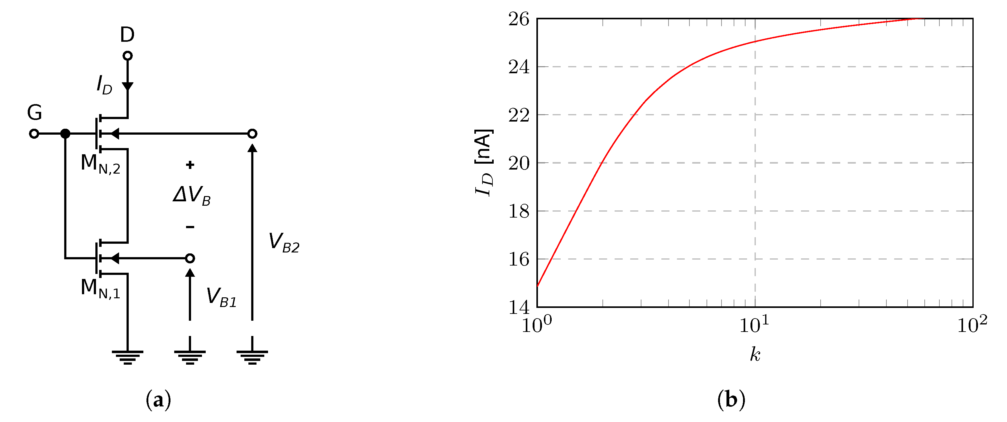
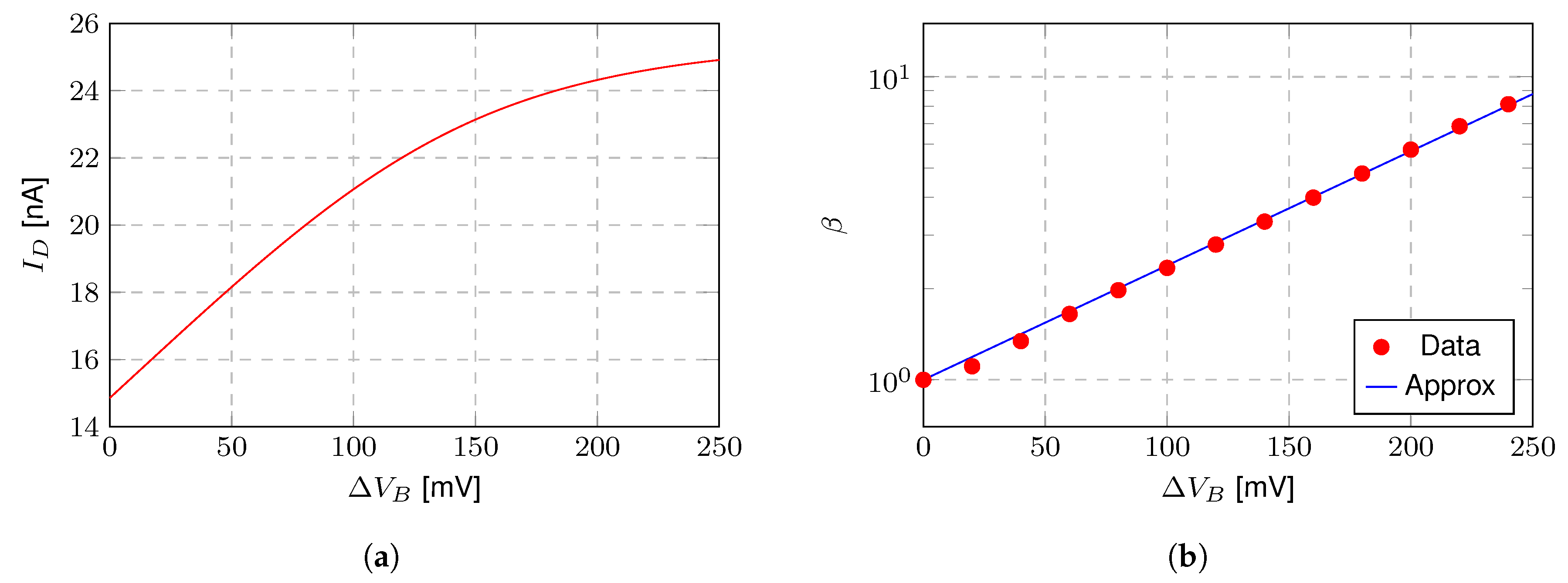
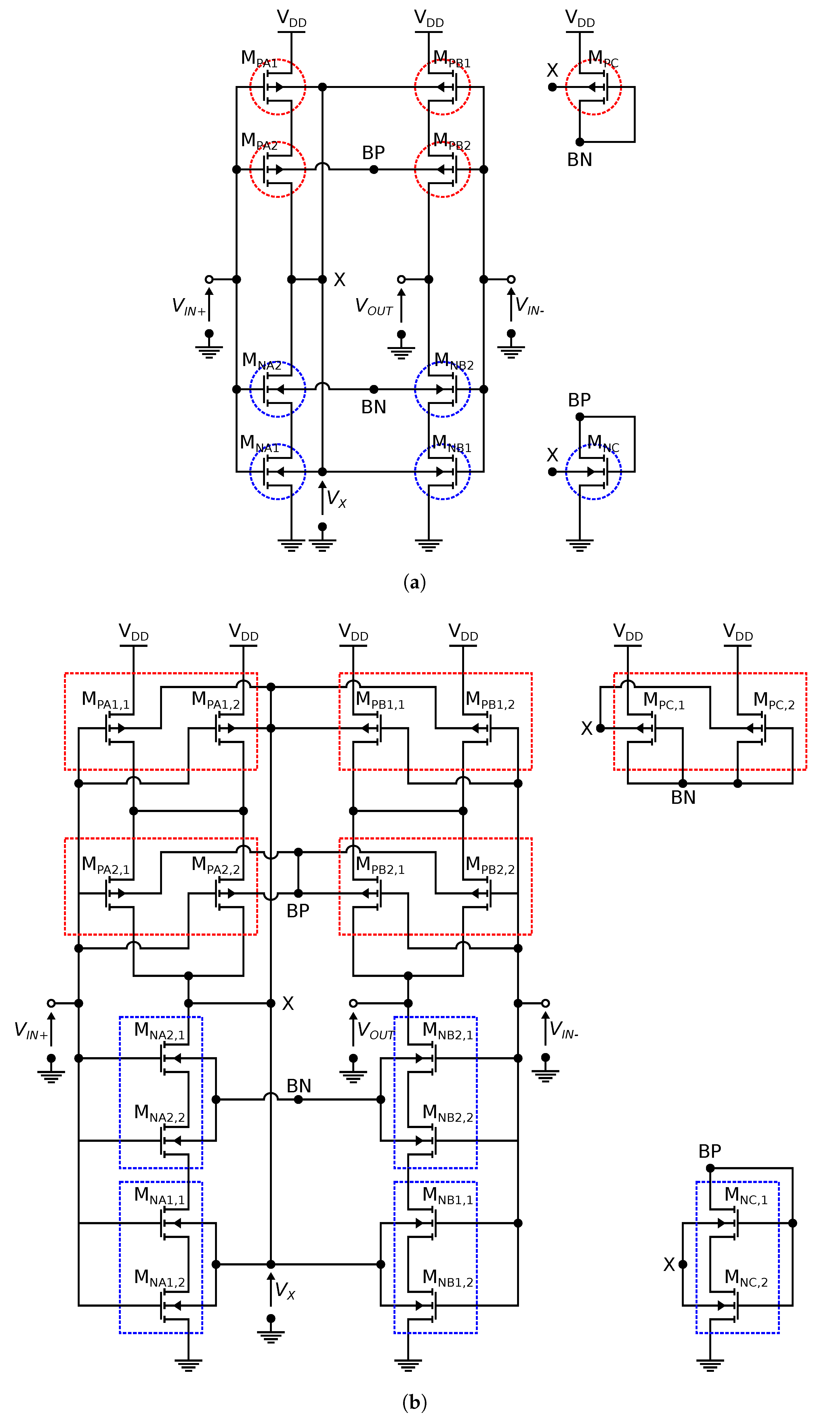
2. Composite Transistor with an Improved Forward-Body-Bias

Implementing inverter-based OTAs with composite transistors allows designers to exploit the gain-area trade-off. Figure 1a represents an elementary composite N-type transistor MN made of two series transistors MN,2 and MN,1. Considering that MN,1 and MN,2 have the same length, the equivalent transistor aspect ratio S e q is defined by (1) [19]:
S e q = W e q L e q = S N , 1 · S N , 2 S N , 1 + S N , 2 = k k + 1 · S N , 1
where
k = S N , 2 S N , 1 = W N , 2 W N , 1
Such use of composite transistors improves voltage gain by increasing the k factor [21], which is the ratio of the transistors MN,2 and MN,1 aspect ratios S N , 2 and S N , 1 . The equivalent transistor channel length L e q and the Early Voltage V A increase proportionally to k; however, the equivalent transistor total area and input capacitance also increase accordingly.
By using the UICM (Unified Current Control Model) all-region transistor model [23] approximation to the weak inversion transistor operation, the transistor drain current I D can be calculated as follows:
I D 2 · I S · e V G B V T n V S B n ϕ t + 1 e V G B V T n V D B n ϕ t + 1
I S = I S H · S = μ C o x n ϕ t 2 2 · W L
where V G B , V S B , and V D B are respectively the the gate-to-bulk, source-to-bulk, and drain-to-bulk voltages, V T is the threshold voltage, n is the slope factor, ϕ t is the thermal voltage, I S is the normalization current, I S H is the sheet normalization current, S is the transistor aspect ratio, μ is the charge mobility, and C o x is the gate oxide capacitance per area.
Considering that I D = I D N , 1 = I D N , 2 and V X = V D N , 1 = V S N , 2 , that MN,1 operates in the linear region, MN,2 operates in the saturation region, and both transistors operate in weak inversion, the composite transistor drain current I D can be calculated as shown in (5) and (6):
I D 2 · I S H · S N , 1 · e V G + ( n 1 ) V B 1 V T n ϕ t + 1 · 1 e V X ϕ t 2 · I S H · S N , 2 · e ( n 1 ) Δ V B n ϕ t · e V G + ( n 1 ) V B 1 V T n ϕ t + 1 · e V X ϕ t
V X ϕ t · ln S N , 1 + S N , 2 · e ( n 1 ) Δ V B n ϕ t S N , 1
By fixing the size of MN,1, the drain current I D can be changed by varying the width of the transistor MN,2, and assuming the body-bias of the of the two series transistors MN,1 and MN,2 in Figure 1a tied at the same voltage, so that V G = V D = V B 1 = V B 2 = 0.25 V, the drain current I D of the composite transistor is proportional to the equivalent transistor aspect ratio, as described in (7) and shown in Figure 1b:
I D 2 · I S H · S e q · e V G + ( n 1 ) V B 1 V T n ϕ t + 1 S e q = S N , 1 · S N , 2 S N , 1 + S N , 2 = k k + 1 · S N , 1
A similar current increase can be reached keeping the size of the two series transistors MN,2 and MN,1 equal ( k = 1 ) and biasing the two transistors independently in Figure 1a [22]. Assuming V G = V D = V B 1 = 0.25 V, Figure 2a shows how the drain current I D can be increased by means of a difference of the body-bias voltage Δ V B = V B 2 V B 1 . Notice that, in this later case, two series transistors MN,2 and MN,1 in Figure 1a have equal size ( k = 1 ) so that the drain current I D can be expressed as:
I D S N , 1 · β S N , 2 S N , 1 + β S N , 2 = β β + 1 · S N , 1
where
β e ( n 1 ) Δ V B n ϕ t
represents a correction factor for the current drain I D definition due to the difference between the body-bias of the series transistors MN,2 and MN,1, assuming the transistors are operating in weak inversion, as can be highlighted comparing (7) with (8). Figure 2b shows how β changes with the difference of the body-bias voltage Δ V B = V B 2 V B 1 , which agrees with the approximation defined by (9) for a slope factor n 1.29 and a thermal voltage ϕ t 26 mV.
Figure 3a shows how the small-signal gate transconductance g m changes by varying k and while keeping Δ V B = 0 ( β = 1 ), and by varying β and keeping k = 1 for V G = V D = V B 1 = 0.25 V. For weak inversion, as expected, g m is proportional to I D , as
g m I D n ϕ t
In addition, the equivalent transistor output resistance r o , the inverse of the output conductance g o , defined by
r o = 1 g o = d V D d I D = V A I D = V E L I D ,
is a function of the Early voltage V A and the drain current I D , considering that the transistor MN,2 operates in the saturation region. The Early voltage is defined by a technology parameter V E and the transistor channel length L. Figure 3c shows that V A increases almost proportionally with k and β , which means that, by this definition, the equivalent transistor channel length L e q increases accordingly.
Figure 3d shows the equivalent transistor small-signal intrinsic voltage gain, which is defined as A V = g m r o . As shown in Figure 3a–d, the small-signal parameters vary almost exactly as a function of k or β , which proves that an improved composite transistor differential forward-body-bias voltage variation is equivalent to a composite transistor physical parameter variation.
In the next section, the above-mentioned differential forward-body-bias, is applied to two novel inverter-based OTAs with composite transistors.

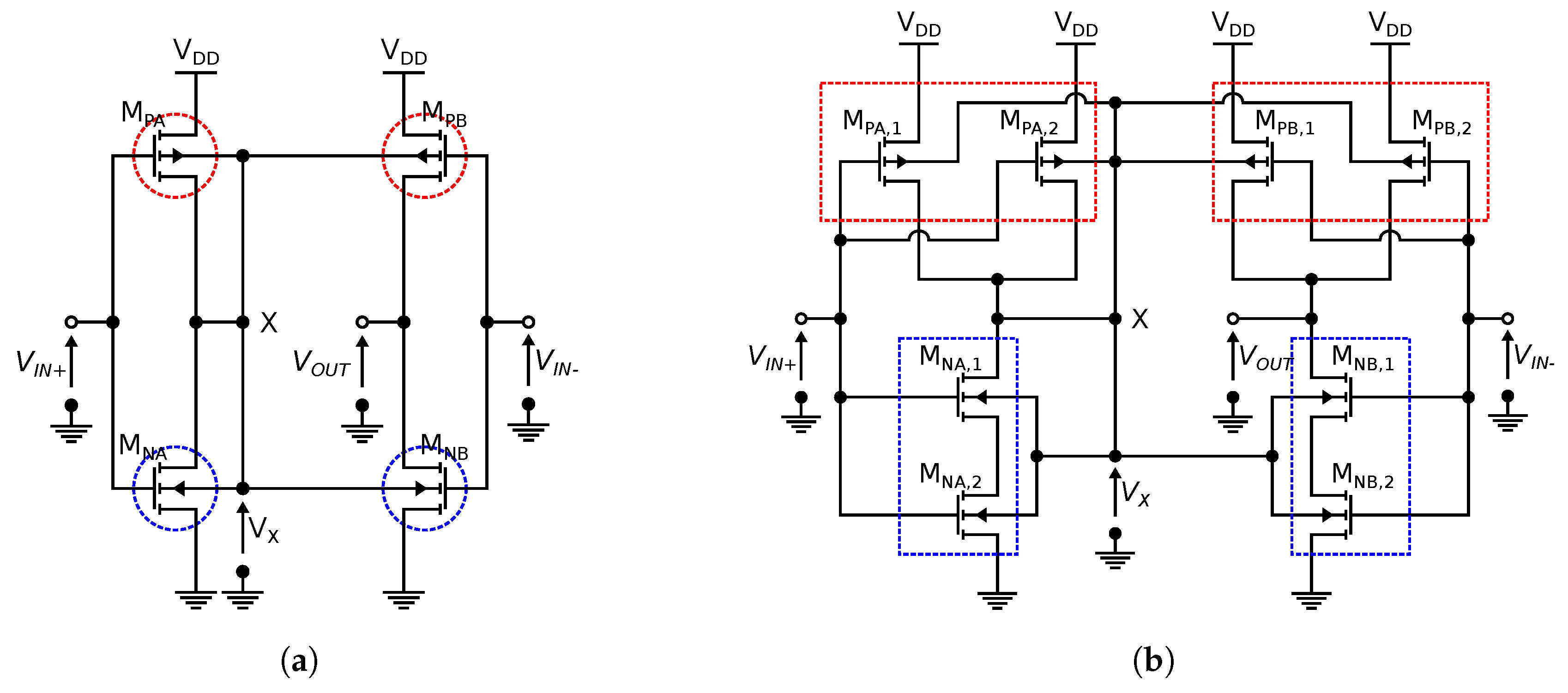
3. Inverter-Based OTAs with an Improved Forward Body-Bias

Figure 4 shows the compact and extended circuit view of the conventional inverter-based, pseudo-differential, single-ended OTA with a forward-body-bias, which is basically the half-circuit of the fully-differential Bulk Nauta OTA proposed in [21].
In order to compensate the charge mobility difference between PMOS and NMOS transistors, the inverter PMOS aspect ratio S P must be greater than the NMOS S N . In this particular design, S P must be approximately four times greater than S N . One way to do that is to keep both PMOS and NMOS transistor lengths L constant and choose a PMOS width W P four times wider than W N . In this design, the inverter is made of PMOS parallel transistor arrays and NMOS series transistor arrays, which saves 20% of the total area.
In particular, the equivalent transistors shown in Figure 4a, the PMOS MPA, MPB, and the NMOS MNA, MNB are respectively parallel and series rectangular transistor arrays represented as the single unit transistors in Figure 4b. The red and blue dashed lines highlight such an equivalence.
In the following, all unit transistors that make up the composite transistors have the same aspect ratio S u . Assuming that the aspect ratios of MNA,1 and MNA,2 are equal, so that
S N , 1 = S N , 2 = S u = W L
the equivalent aspect ratio of the N-type rectangular transistor array is
S N = W N L N = W 2 · L = S u 2
and its equivalent active area is A T N = 2 A u where A u is the area ( W · L ) of the unit transistor.
Similarly, every P-type rectangular transistor array MP is made of two parallel unit transistors of the same aspect ratio S u . Thus, it has an equivalent aspect ratio that is equal to
S P = W P L P = 2 · W L = 2 · S u
and an equivalent active area equal to A T P = 2 A u .
The two branches of this OTA (named OTA-A in the following) are made of P-type (MPA, MPB a) and N-type (MNA, MNB) transistors whose bulk terminals are all connected to the node X (see Figure 4a). This way, both the P- and N-type transistors MP and MN bulk terminals of the two branches of the OTA-A are biased at V X V D D / 2 = 0.15 V for typical process parameters.
As the fully differential Bulk Nauta OTA [21], this topology has a limited common-mode rejection and requires additional area required for the guard rings needed to isolate the substrate, so that the overall area is larger than the area of two conventional inverters only. In addition, since the NMOS transistors are independently forward-body-biased, a triple well CMOS process is required.
Based on this topology, a version of the former OTA using improved composite transistors to further increase the voltage gain is proposed, as shown in Figure 5. Similarly to Figure 4a,b, Figure 5a,b represent the compact and extended circuit view of the proposed improved version of the former circuit in Figure 4, where the pull-up and pull-down network are made of improved composite transistors, and each transistor array is equivalently represented by single unit transistors.
In the proposed OTA-B, a modified version of improved composite transistor from [22] is used to independently bias the body of the composite transistors with a differential bulk terminal voltage Δ V B . Instead of being tied to the input nodes of the inverters, as in [22], the bulk terminals of the transistors MPA-B,2 and MNA-B,2 are tied respectively to the diode-connected transistors MNC and MPC, so that their voltages are respectively almost equal to zero or to the supply voltage, but the parasitic substrate current is limited [21].
Then, the bulks of the transistors MPA-B,1 and MNA-B,1 are tied to the node X, which voltage is V x V D D / 2 = 0.15 V.
On this basis, each improved composite transistor that defines the pull-up and pull-down network of the OTA-B has a forward-body-bias differential voltage Δ V B V D D / 2 = 0.15 V, which is the aim of the design.
Notice that these transistors (MPC and MNC) are not required when using a FD-SOI CMOS technology process [24] as this technology offers isolated transistors with a built-in insulator between the substrate and the transistor channel. Moreover, there is no parasitic substrate current by using forward-body-biasing in FD-SOI technologies.
The width W of each unit transistor, both in the OTA-A and OTA-B, is set on the basis of the minimum sizing requirement of the isolated n-well and p-well. Based on this, all the unit transistors, both PMOS and NMOS, in OTA-A and OTA-B (see Figure 4b and Figure 5b) have an identical aspect ratio equal to
W L N = W L P = 1.26 μ m 0.42 μ m
The layouts of the OTA-A and OTA-B are shown in Figure 6a,b, respectively. These figures depict how systematic mismatch reduction layout techniques, such as common centroid and dummy transistors, were employed in both OTAs. The name of the unit transistor are placed on top of each instance in the layout.

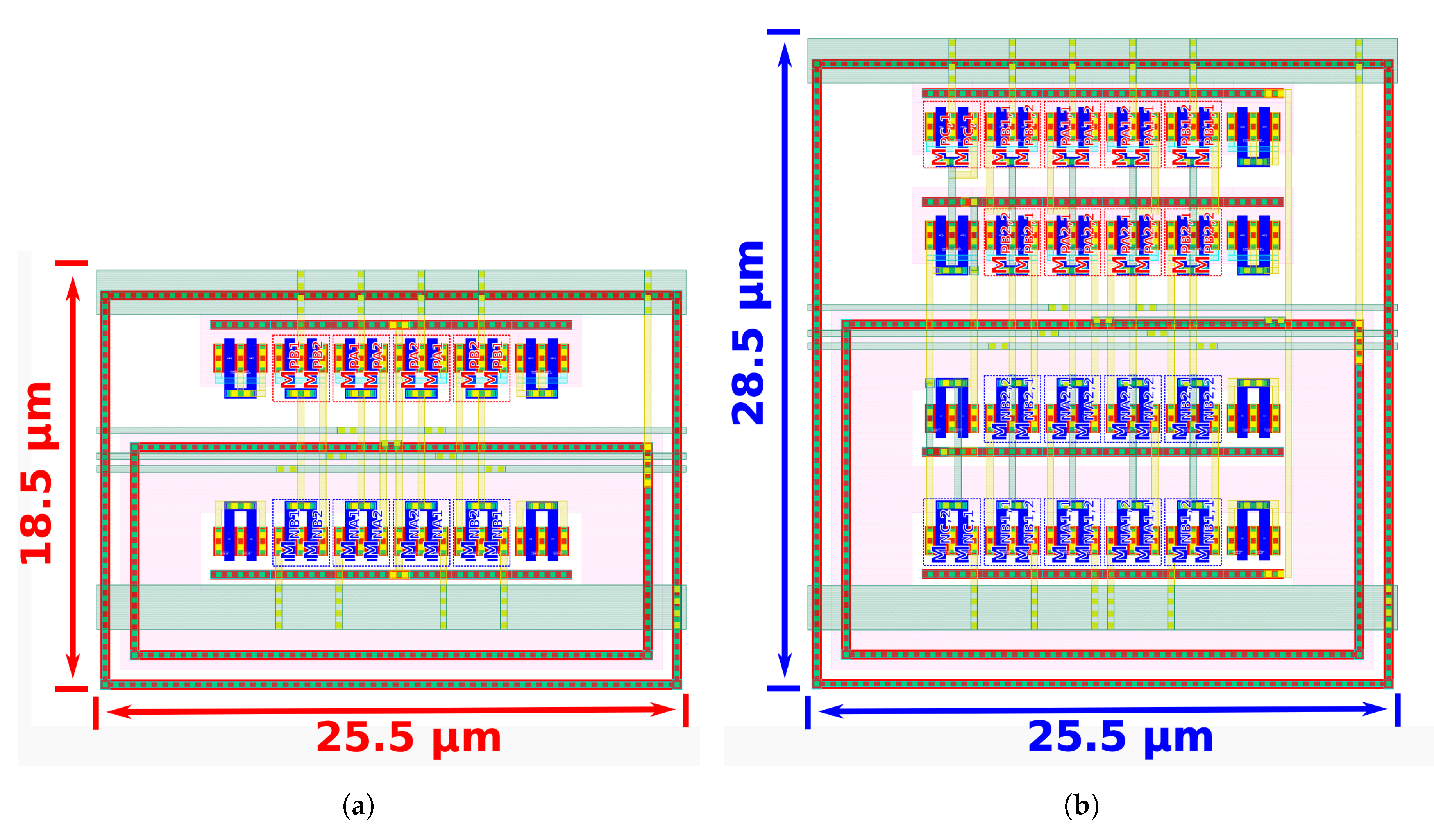
4. Simulation Results

The performance of both OTA-A and OTA-B, designed in TSMC 180 nm CMOS technology, operating at 27 ° C, 0.3 V supply voltage, has been validated by using an open-loop and a non-inverting buffer OTA test-bench circuits with a 10 pF capacitive load C L . Circuits are respectively shown in Figure 7a,b. These two test-benches are aimed to characterize input and output voltage swings, and output voltage linearity of OTAs.
Simulations results reported in Section 4.1 and Section 4.2 refer respectively to the open-loop and the non-inverting buffer OTA test-bench circuits as shown in Figure 7a,b.

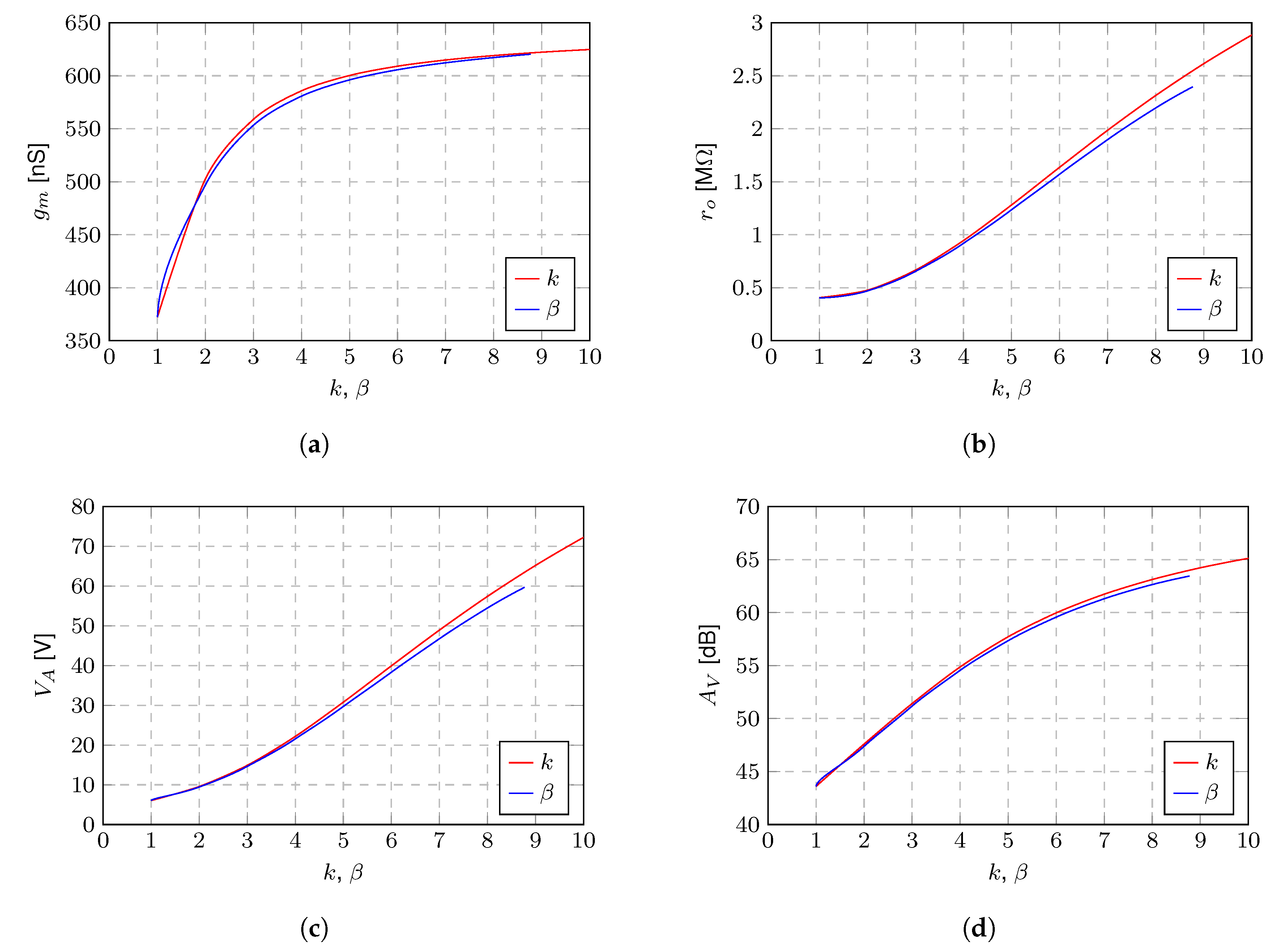
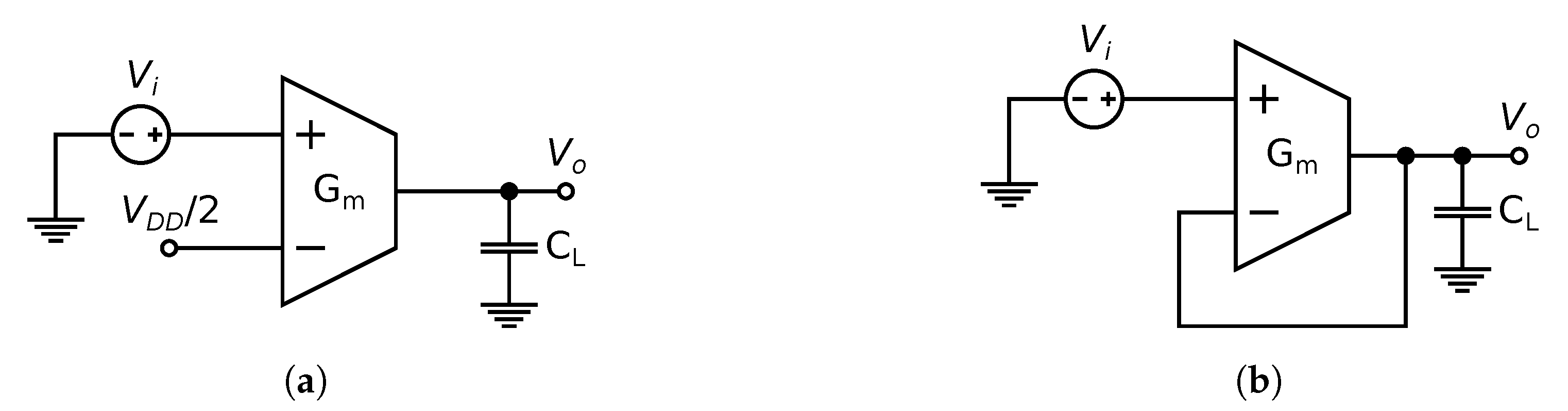
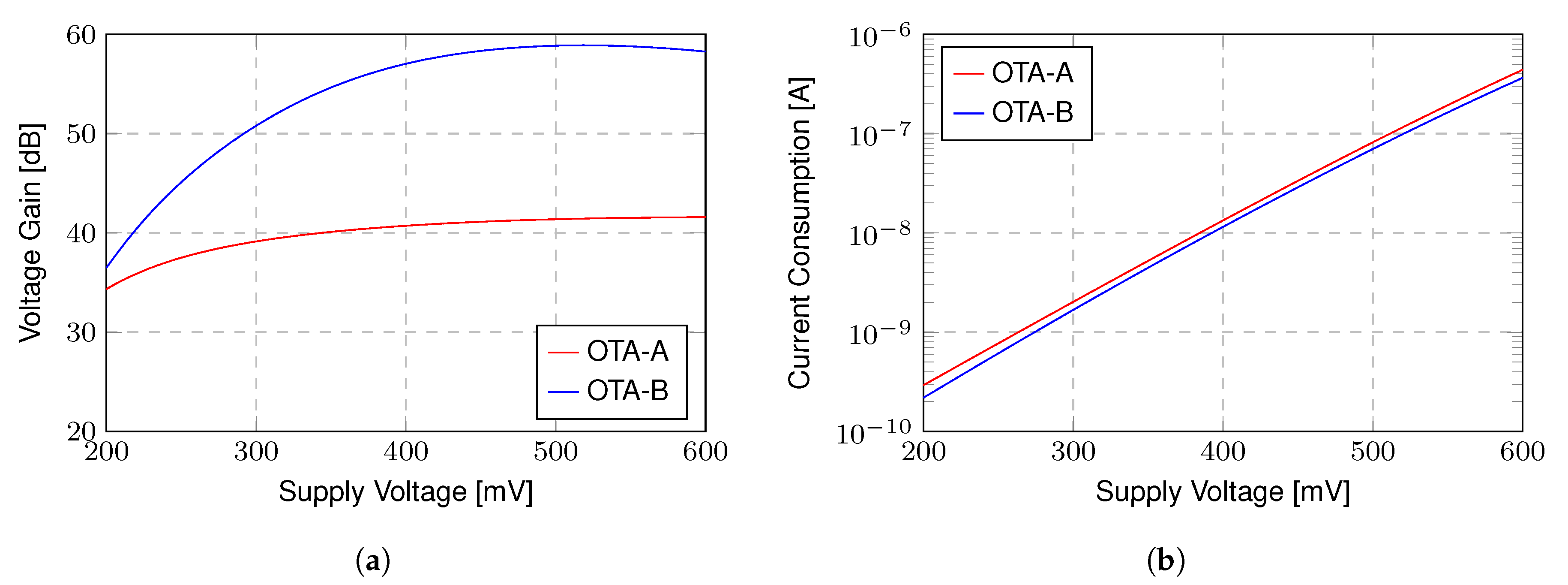
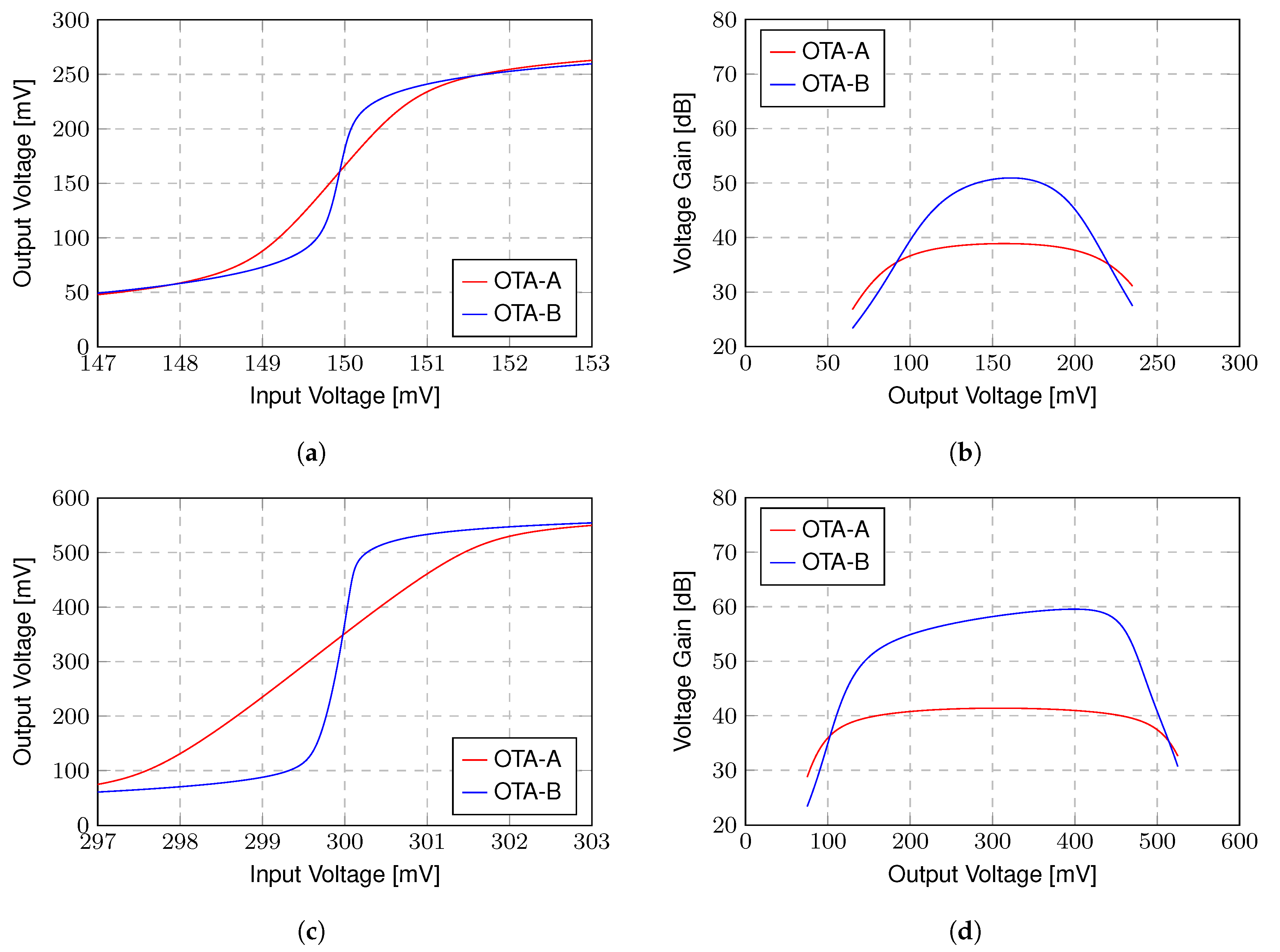
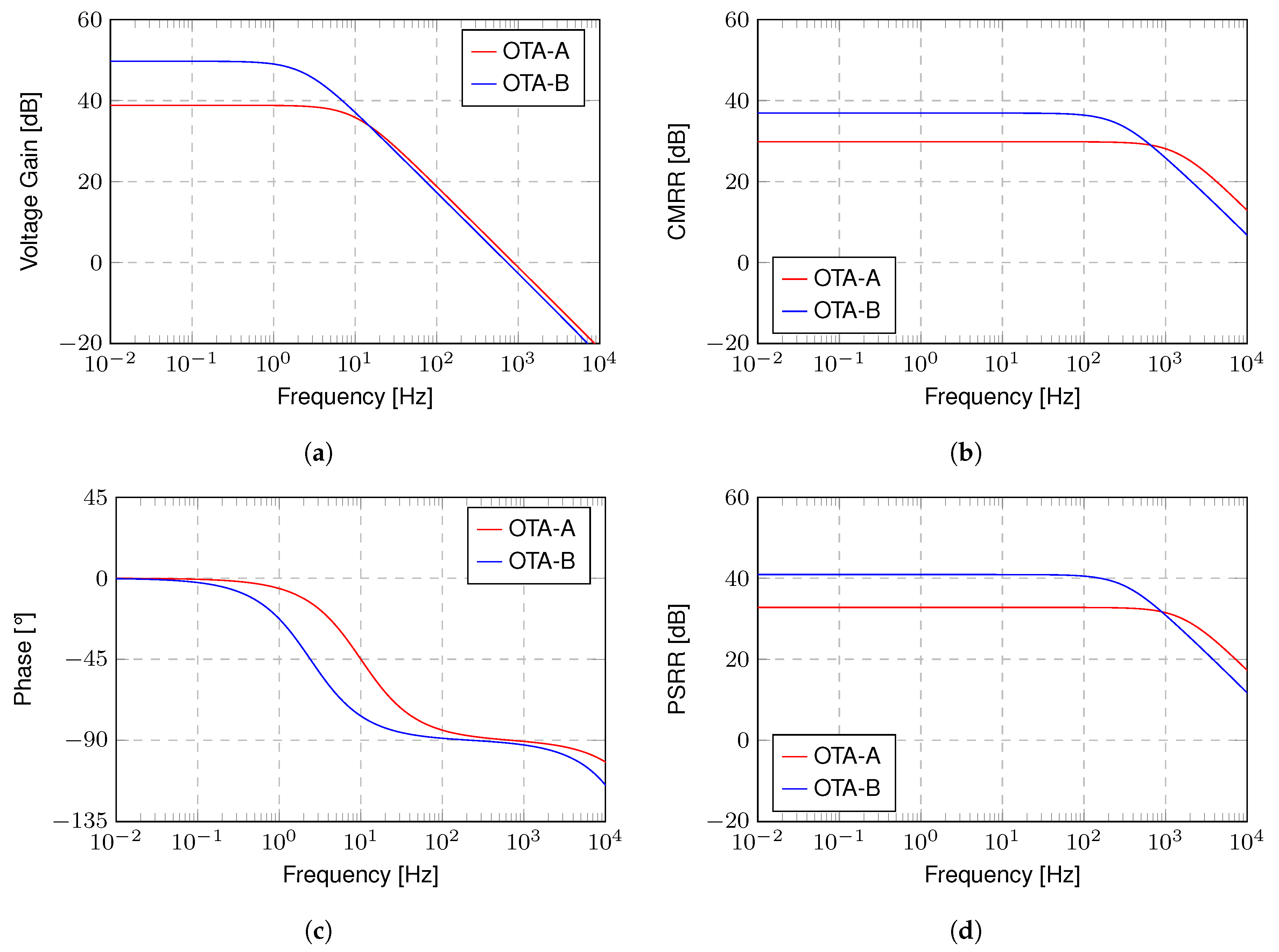
4.1. Open-Loop Analysis

Figure 8 shows how gain and power consumption are affected by the supply voltage variation. It shows how, on the basis of their inverter-based nature, both of the two OTAs are suitable to face voltage/power trade-off as well as operate at the near-threshold voltage. In particular, Figure 8a evince how voltage gains of OTA-A and OTA-B react supply voltage variations from 0.6 V down to 0.2 V. For a supply voltage V D D equal to 0.2 V, OTA-A and OTA-B have approximately the same voltage gain. As V D D increases, at a 0.3 V supply voltage, OTA-A and OTA-B have respectively a voltage gains equal to 39 and 51 dB. A further increment of the supply voltage V D D produce a negligible gain improvement for V D D higher than 0.4 V. Figure 8b depicts the exponential increment of the current consumption with the voltage supply. Notice that the OTAs are self-biased, thus no extra power consumption related to additional voltage/current reference current has to be considered.
The reported results refer to an input voltage equal to V D D / 2 where the voltage gain assumes the maximum value. Moreover, the supply voltage affects the OTAs’ gains as a consequence of the reverse transistor current and channel length modulation [23]. For these reasons, Figure 9a,b respectively show the proposed OTAs input–output characteristic and the gain of the OTAs versus output voltage for a voltage supply V D D = 0.3 V. Figure 9c,d show the same for V D D = 0.6 V.
Figure 9b shows output voltage swings from between 100 mV and 200 mV for both OTAs, supplied with V D D = 0.3 V, as either PMOS or NMOS transistors begin to operate in the linear region. Similarly, for a supply voltage V D D = 0.6 V, the valid output voltage swings in the range from 100 mV to 500 mV.
Figure 10a–d show the AC differential voltage gain, CMRR, output phase and PSRR curves, respectively. As expected, OTA-A and OTA-B have similar GBW of 904 and 704 Hz, respectively. As both of the OTAs are single-stage amplifiers, their phase margins are 90º. The common-mode rejection ratios (CMRR) for OTA-A and OTA-B are 30 and 37 dB, and power supply rejection ratios are 33 and 41 dB, respectively.
Figure 11 shows the equivalent input referred noise for each OTA. OTA-A and OTA-B respectively have equivalent input noises of 784 and 809 nV/ Hz , at 1 kHz. The flicker noise is similar in both OTAs.

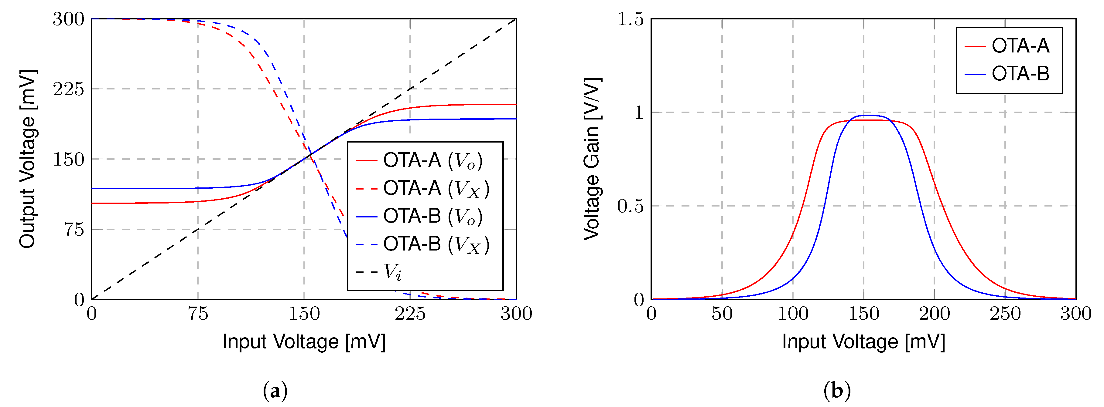
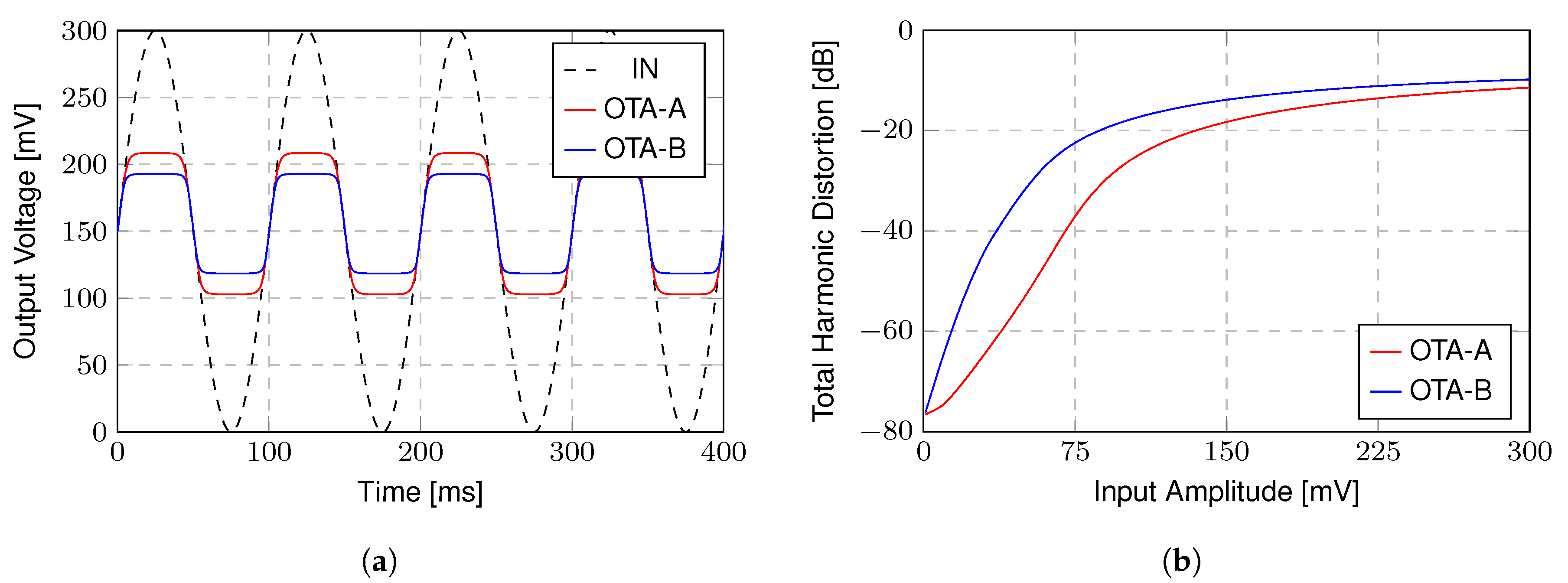
4.2. Unity-Gain Buffer Analysis

As with the output voltage swing limitations observed in open-loop DC simulations (as in Figure 7a), the non-inverting buffer simulations (as in Figure 7) also reveal the limits of input voltage swing, which are shown in Figure 12.
In particular, Figure 12a shows how the output voltage saturation is a consequence of the voltage gain from the input IN+ to node X. As can be seen, V X A V X ( V I N + V D D / 2 ) + V D D / 2 and A V X 1 / ( n 1 ) for OTA-A, where A V X is the voltage gain between V X and V I N + . This means that the positive input voltage range is limited to approximately V D D / 2 ± ( n 1 ) V D D / 2 . This effect is explained in more detail [21] for the OTA-A fully differential counterpart, the Bulk Nauta OTA. The OTA-B has a slightly shorter input range, since one of the composite transistor bulk terminals are biased by the voltage supply instead of V X and does not contribute to common-mode voltage rejection.
The same limitations, from the point of view of time-domain, are shown in Figure 13a for a rail-to-rail input sine-wave. The corresponding total harmonic distortion (THD) is displayed in Figure 13b. A total harmonic distortion of 1% is achieved for input ranges of 70 mV and 35 mV in OTA-A and OTA-B, respectively.

4.3. Monte Carlo Simulation Results

Table 1 summarizes the mean μ and the standard variation σ from 1000 Monte Carlo simulation runs. Process and mismatch variations are analyzed individually and combined.
Results show that gain-bandwidth product GBW, total current I D D , and power consumption are greatly affected by the process variability. This also results from not using current references for biasing the OTAs. The power efficiency Figure of Merit FoM, defined as 100 × ( GBW · C L ) / I D D , shows a negligible variation. It is the same for the open-loop voltage gain. As a main drawback, the mismatch variations strongly affect the offset voltage V OS of both OTAs. The simulations show 6.3 and 5.4 mV input offset voltage for 3 σ mismatch variation for OTA-A and OTA-B, respectively. Such effect could be compensated by an additional calibration network [25] or by increasing the transistor arrays’ sizes [20].
Table 2 summarizes the corner simulation results. As expected, the greatest deviations from typical corner results are GBW and power for SS (Slow-Slow) and FF (Fast-Fast) corners, and the intrinsic input offset voltage for SF (Slow-Fast) and FS (Fast-Slow) corners.

4.4. Performance Comparison

The proposed OTAs are gate input-driven, single-ended, and single-stage and therefore offer compact layouts and power efficiency. The characteristics are summarized and compared with the state of the art in Table 3. The proposed OTA-A is a single-ended version of the fully-differential bulk-nauta OTA presented in [21] that uses conventional composite transistors to increase its voltage gain. Thus, OTA-A would offer similar performance with 2× less area and power consumption.
Bulk-driven OTAs, like those proposed in [8,9,10,11,18], are intrinsically more linear and have a larger input voltage range than its gate-driven OTAs counterparts. However, those OTAs deliver a lower transconductance for a given power consumption as can be highlighted from their Figure of Merit (FoM). In addition, bulk-driven OTAs have finite DC input impedance, which could affect previous gain stages. The proposed OTA linearity is limited by the input–voltage excursion, as explained in the previous sections. The THD of both OTA-A and OTA-B are comparable to the other gate-driven inverter-based OTAs shown in the table and their FoMs are the second best after [25], which use extra digital-assisted circuitry.
Multiple-stage OTAs show higher voltage gains at the cost of area and power consumption. Additionally, they need frequency stability circuits to work properly with negative feedback circuits, which costs even more area and power. The OTAs proposed in [9,10,11,18] are multiple stage OTAs whose first stages are bulk-driven OTAs and the subsequent stages are gate-driven OTAs, which combines the linearity and input range of the bulk-driven OTAs and the voltage gain of gate-driven OTAs. The proposed OTAs have a greater voltage gain than all single-stage OTAs, with the exception of the OTA proposed in [21], which uses larger composite transistors and operates at a higher supply voltage. Most of the presented multiple-stage OTAs have a greater voltage-gain, but their voltage gain over the number of stages are below those of the proposed OTAs.

5. Conclusions

This paper introduces two inverter-based OTA topologies to increase the voltage gain without reducing output voltage swing and with a minor linearity degradation for ultra-low-voltage supplies. Proposed OTAs exploit two topological solutions consist of using rectangular arrays for PMOS and NMOS charge mobility balancing and forward-body biasing for common-mode rejection. For analyzing the contribution of each solution individually, OTA-A has been designed as a conventional inverter-based single-end OTA whose equivalent pull-up and pull-down networks are made of rectangular transistor arrays to achieve the smallest area possible. On the other hand, the OTA-B design allies the properties of such rectangular transistors to the improved composite transistor with independent body-bias.
The bulk terminals of the two rectangular transistor arrays which compose the improved composite transistor (pull-up and pull-down network of each branch of the OTA-B) are tied to different voltages. This provides an enhancement of 11 dB on voltage gain for a supply voltage equal to V D D = 0.3 V, which is equivalent to the voltage gain enhancement of a conventional composite transistor with 2.5× area increase.
Compared with other state-of-art OTAs in similar operation conditions, the proposed OTAs have the largest voltage gain by the number of amplifier gain stages (39 and 51 dB), smallest die-area (472 and 727 μm2), and is among the most power-efficient (447 and 443 V−1 FoM). The improved self-cascode technique applied to composite transistors can be extended to other inverter-based topologies such as multiple-stage and fully-differential OTAs. Moreover, the same technique can exploit the FD-SOI technologies ability of providing forward-body-bias at higher supply voltages.

Author Contributions

Conceptualization, L.H.R.; methodology, L.H.R., and O.A.; validation, L.H.R.; formal analysis, L.H.R., O.A.; investigation, L.H.R.; resources, C.R.R.; data curation, L.H.R.; writing—original draft preparation, L.H.R.; writing—review and editing, O.A. and C.R.R.; visualization, L.H.R.; supervision, O.A. and C.R.R.; project administration, C.R.R.; funding acquisition, C.R.R. All authors have read and agreed to the published version of the manuscript.

Funding

This research was funded by Coordenação de Aperfeiçoamento de Pessoal de Nível Superior (CAPES).

Acknowledgments

The authors would like to thank Europractice and TSMC for PDK access. The authors thank Pedro Toledo for the helpful suggestions.

Conflicts of Interest

The authors declare no conflict of interest.

Abbreviations

The following abbreviations are used in this manuscript:
CMOSComplementary Metal-Oxide-Semiconductor
CMRRCommon-Mode Rejection Ratio
DPDifferential Pair
FoMFigure of Merit
GBWGain-Bandwidth-Product
NMOSN-type Metal-Oxide-Semiconductor
OTAOperational Transconductance Amplifier
PMOSP-type Metal-Oxide-Semiconductor
PSRRPower Supply Rejection Ratio
THDTotal Harmonic Distortion
UICMUnified Current Control Model
ULPUltra-Low-Power
ULVUltra-Low-Voltage

References

  1. Kim, S.; Vyas, R.; Bito, J.; Niotaki, K.; Collado, A.; Georgiadis, A.; Tentzeris, M.M. Ambient RF Energy-Harvesting Technologies for Self-Sustainable Standalone Wireless Sensor Platforms. Proc. IEEE 2014, 102, 1649–1666. [Google Scholar] [CrossRef]
  2. Aiello, O.; Crovetti, P.; Alioto, M. A Sub-Leakage pW-Power Hz-Range Relaxation Oscillator Operating with 0.3 V–1.8 V Unregulated Supply. In Proceedings of the IEEE 2018 Symposia on VLSI Circuits (VLSI 2018), Honolulu, HI, USA, 18–22 June 2018; pp. 119–120. [Google Scholar]
  3. Aiello, O.; Crovetti, P.; Lin, L.; Alioto, M. A pW-Power Hz-Range Oscillator Operating With a 0.3–1.8-V Unregulated Supply. IEEE J. Solid-State Circuits 2019, 54, 1487–1496. [Google Scholar] [CrossRef]
  4. Bertacchini, A.; Larcher, L.; Maini, M.; Vincetti, L.; Scorcioni, S. Reconfigurable RF Energy Harvester with Customized Differential PCB Antenna. J. Low Power Electron. Appl. 2015, 5, 257–273. [Google Scholar] [CrossRef] [Green Version]
  5. Aiello, O.; Crovetti, P.; Alioto, M. Fully Synthesizable Low-Area Digital-to-Analog Converter with Graceful Degradation and Dynamic Power-Resolution Scaling. IEEE Trans. Circuits Syst. I Regul. Pap. 2019, 66, 2865–2875. [Google Scholar] [CrossRef]
  6. Aiello, O.; Crovetti, P.; Alioto, M. Fully Synthesizable Low-Area Analogue-to-Digital Converters with Minimal Design Effort Based on the Dyadic Digital Pulse Modulation. IEEE Access 2020, 8, 70890–70899. [Google Scholar] [CrossRef]
  7. Richelli, A.; Colalongo, L.; Kovacs-Vajna, Z.; Calvetti, G.; Ferrari, D.; Finanzini, M.; Pinetti, S.; Prevosti, E.; Savoldelli, J.; Scarlassara, S. A Survey of Low Voltage and Low Power Amplifier Topologies. J. Low Power Electron. Appl. 2018, 8, 22. [Google Scholar] [CrossRef] [Green Version]
  8. Chatterjee, S.; Tsividis, Y.; Kinget, P. 0.5-V analog circuit techniques and their application in OTA and filter design. IEEE J. Solid-State Circuits 2005, 40, 2373–2387. [Google Scholar] [CrossRef]
  9. Ferreira, L.H.; Sonkusale, S.R. A 60-dB gain OTA operating at 0.25-V power supply in 130-nm digital CMOS process. IEEE Trans. Circuits Syst. I Regul. Pap. 2014, 61, 1609–1617. [Google Scholar] [CrossRef]
  10. Abdelfattah, O.; Roberts, G.W.; Shih, I.; Shih, Y.C. An ultra-low-voltage CMOS process-insensitive self-biased OTA with rail-to-rail input range. IEEE Trans. Circuits Syst. I Regul. Pap. 2015, 62, 2380–2390. [Google Scholar] [CrossRef]
  11. Veldandi, H.; Shaik, R.A. A 0.3-v pseudo-differential bulk-input ota for low-frequency applications. Circuits Syst. Signal Process. 2018, 37, 5199–5221. [Google Scholar] [CrossRef]
  12. Veeravalli, A.; Sánchez-Sinencio, E.; Silva-Martínez, J. Transconductance amplifier structures with very small transconductances: A comparative design approach. IEEE J. Solid-State Circuits 2002, 37, 770–775. [Google Scholar] [CrossRef] [Green Version]
  13. Nauta, B. A CMOS transconductance-C filter technique for very high frequencies. IEEE J. Solid-State Circuits 1992, 27, 142–153. [Google Scholar] [CrossRef] [Green Version]
  14. Barthelemy, H.; Meillere, S.; Gaubert, J.; Dehaese, N.; Bourdel, S. OTA based on CMOS inverters and application in the design of tunable bandpass filter. Analog Integr. Circuits Signal Process. 2008, 57, 169–178. [Google Scholar] [CrossRef]
  15. Vlassis, S. 0.5 V CMOS inverter-based tunable transconductor. Analog Integr. Circuits Signal Process. 2012, 72, 289–292. [Google Scholar] [CrossRef]
  16. Vieru, R.G.; Ghinea, R. An ultra low voltage sigma delta modulator with inverter based scalable amplifier. In Proceedings of the 2012 10th International Symposium on Electronics and Telecommunications, Timisoara, Romania, 15–16 November 2012; pp. 3–6. [Google Scholar]
  17. Khateb, F.; Kulej, T.; Vlassis, S. Extremely low-voltage bulk-driven tunable transconductor. Circuits Syst. Signal Process. 2017, 36, 511–524. [Google Scholar] [CrossRef]
  18. Baghtash, H.F. A 0.4 V, body-driven, fully differential, tail-less OTA based on current push-pull. Microelectron. J. 2020, 99, 104768. [Google Scholar] [CrossRef]
  19. Galup-Montoro, C.; Schneider, M.C.; Loss, I.J. Series-parallel association of FET’s for high gain and high frequency applications. IEEE J. Solid-State Circuits 1994, 29, 1094–1101. [Google Scholar] [CrossRef]
  20. Braga, R.A.; Ferreira, L.H.; Coletta, G.D.; Dutra, O.O. A 0.25-V calibration-less inverter-based ota for low-frequency gm-c applications. Microelectron. J. 2019, 83, 62–72. [Google Scholar] [CrossRef]
  21. Rodovalho, L.H. Push–pull based operational transconductor amplifier topologies for ultra low voltage supplies. Analog. Integr. Circuits Signal Process. 2020, 1–14. [Google Scholar] [CrossRef]
  22. Niranjan, V.; Kumar, A.; Jain, S.B. Composite transistor cell using dynamic body bias for high gain and low-voltage applications. J. Circuits Syst. Comput. 2014, 23, 1450108. [Google Scholar] [CrossRef]
  23. Schneider, M.C.; Galup-Montoro, C. CMOS Analog Design Using All-Region MOSFET Modeling; Cambridge University Press: Cambridge, UK, 2010. [Google Scholar]
  24. Clerc, S. The Fourth Terminal: Benefits of Body-Biasing Techniques for FDSOI Circuits and Systems; Springer Nature Switzerland AG: Cham, Switzerland, 2020. [Google Scholar]
  25. Toledo, P.; Aiello, O.; Crovetti, P. A 300mV-Supply Standard-Cell-Based OTA with Digital PWM Offset Calibration. In Proceedings of the IEEE Nordic Conference of Circuits and Systems, Helsinki, Finland, 29–30 October 2019. [Google Scholar]
  26. Lv, L.; Zhou, X.; Qiao, Z.; Li, Q. Inverter-Based Subthreshold Amplifier Techniques and Their Application in 0.3-V Delta Sigma Modulators. IEEE J. Solid-State Circuits 2019, 54, 1436–1445. [Google Scholar] [CrossRef]
  27. Manfredini, G.; Catania, A.; Benvenuti, L.; Cicalini, M.; Piotto, M.; Bruschi, P. Ultra-Low-Voltage Inverter-Based Amplifier with Novel Common-Mode Stabilization Loop. Electronics 2020, 9, 1019. [Google Scholar] [CrossRef]
Figure 1. N-MOS composite transistor: (a) schematic; (b) drain current ID versus the aspect ratio k variation of the transistors MN,2 and MN,1 for VG = VD = VB1 = VB2 = 0.25 V (ΔVB = VB2VB1 = 0).
Electronics 09 01410 g001
Figure 2. N-MOS composite transistor: (a) drain current ID versus body-bias variation ΔVB = VB2VB1 = 0 for equal size of the transistors MN,2 and MN,1 in Figure 1a (k = 1); (b) correction factor β versus body-bias variation ΔVB = VB2VB1 for equal size of the transistors MN,2 and MN,1 in Figure 1a (k = 1).
Electronics 09 01410 g002
Figure 3. Small signal parameters k and β equivalence: (a) transconductance gm (b) output resistance ro (c) early voltage VA and (d) intrinsic voltage gain (AV).
Electronics 09 01410 g003
Figure 4. Proposed inverter-based operational transconductance amplifier (OTA) with forward-body-bias common-mode rejection: (a) basic and (b) extended circuit diagram with the respective rectangular transistors highlighted.
Electronics 09 01410 g004
Figure 5. Proposed inverter-based OTA with forward-body-bias common-mode rejection and improved composite transistors: (a) compact and (b) extended circuit diagram.
Electronics 09 01410 g005
Figure 6. Layouts of the proposed inverter-based OTAs with improved forward-body-bias: (a) with single transistors for the pull-down and pull-up network (OTA-A) and (b) with improved composite transistors for the pull-down and pull-up network (OTA-B).
Electronics 09 01410 g006
Figure 7. OTAs testbench circuits: (a) Open-Loop (Gm-C Integrator); (b) Non-Inverting Buffer.
Electronics 09 01410 g007
Figure 8. Voltage supply dependence: (a) voltage gain; (b) total current consumption.
Electronics 09 01410 g008
Figure 9. DC open-loop results: (a) input–output characteristic for VDD = 0.3 V; (b) voltage gain for VDD = 0.3 V; (c) input–output characteristic for VDD = 0.6 V; (d) voltage gain for VDD = 0.6 V.
Electronics 09 01410 g009
Figure 10. Open-loop AC simulation results: (a) voltage gain; (b) CMRR; (c) phase; (d) PSRR.
Electronics 09 01410 g010
Figure 11. Input referred noise.
Electronics 09 01410 g011
Figure 12. Non-inverting bufferDCsimulation results: (a) input–output characteristic and (b) voltage gain.
Electronics 09 01410 g012
Figure 13. Non-inverting buffer transient simulation results: (a) sine-wave output response; (b) total harmonic distortion.
Electronics 09 01410 g013
Table 1. Monte Carlo results.
GBW [Hz]IDD [nA]FoM [V−1]AV [dB]VOS [mV]Power [pW]
μ σ μ σ μ σ μ σ μ σ μ σ
ProcessOTA-A9472772.10.64471390.10.20.3635186
OTA-B7702261.70.54432510.40.20.4520152
MismatchOTA-A905382.00.144712390.10.12.160718
OTA-B744261.80.044311510.50.11.850312
AllOTA-A9452892.10.644813390.20.12.1633193
OTA-B7787781.80.544311500.70.21.8527154
Table 2. Corner results.
GBW [Hz]IDD [nA]FoM [V−1]AV [dB]VOS [mV]Power [pW]
TTOTA-A9042.044739−0.2607
OTA-B7431.744351−0.1503
SSOTA-A3260.7449400.0218
OTA-B2630.6443500.0178
SFOTA-A9412.145139−1.7626
OTA-B6661.446450−4.3430
FSOTA-A8992.0448390.8603
OTA-B7351.6448481.1492
FFOTA-A24235.444839−0.31624
OTA-B19714.444451−0.21330
Table 3. Perfomance comparison.
[8] +[26] *[20] +[25] *[27] *[21] *[8] +[9] +[10] +[11] *[18] *OTA-A *OTA-B *Unit
Technology1801301301801801801801306565180180180nm
InputGDGDGDGDGDGDBDBDBDBDBDGDGD-
OutputFDFDFDSEFDFDFDSEFDSEFDSESE-
N. of Stages2212112232211-
Die Area17,000-52,0001426800-26,00083,000500030005000472727μm²
VDD0.50.30.250.30.30.50.50.250.350.30.40.30.3V
Power75,000180055210.514017,0001817,000513000.600.50nW
Voltage Gain62502535236452604360813951dB
V. Gain/ N. Stages31252518236426301430413951dB
CMRR75-43--5478-461261263037dB
PSRR81-47--5176-3590793341dB
Offset Voltage6.0-----9.08.4-7.3-6.35.4mV
Input R. Noise22538139---2253300-2820213784809nV/ Hz
THD1-0.13--10.20.3--11%
Input Range712-19100--400150---7035mV
GBW10,00091007.230.898.010036001.88360070280.40.900.74kHz
Phase Margin607690768690 535653599090°
CL2023080101020153551010pF
FoM133303143102022937022292220187447443V−1
+ Measured, * Simulated, GD: Gate-Driven, BD: Bulk-Driven, FD: Fully-Differential, SE: Single-Ended.

