
A Switched Capacitor Memristor Emulator Using Stochastic Computing †
by
 , , , and
Carola de Benito
1,2 ,
,
Oscar Camps
1 ,
,
Mohamad Moner Al Chawa
3,
Stavros G. Stavrinides
4 and
and
Rodrigo Picos
1,2,*
1
Industrial Engineering and Construction Department, Balearic Islands University, 07122 Palma, Spain
2
Health Institute of the Balearic Islands, 07121 Palma, Spain
3
Institute of Circuits and Systems, Technical University of Dresden, 01062 Dresden, Germany
4
School of Science and Technology, International Hellenic University, 57001 Thessaloniki, Greece
*
Author to whom correspondence should be addressed.
†
This paper is an extended version of our paper published in de Benito, C.; Camps, O.; Al Chawa, M.M.; Stavrinides, S.G.; Picos, R. A Stochastic Switched Capacitor Memristor Emulator. 2021 10th International Conference on Modern Circuits and Systems Technologies (MOCAST). IEEE, 2021.
Technologies 2022, 10(2), 39; https://0-doi-org.brum.beds.ac.uk/10.3390/technologies10020039
Submission received: 1 December 2021
/
Revised: 21 January 2022
/
Accepted: 15 February 2022
/
Published: 2 March 2022
(This article belongs to the Special Issue MOCAST 2021)
Abstract
:Due to the increased use of memristors and their many applications, the use of emulators has grown in parallel to avoid some of the difficulties presented by real devices, such as variability and reliability. In this paper, we present a memristive emulator designed using a switched capacitor (SC), that is, an analog component/block and a control part or block implemented using stochastic computing (SCo) and therefore fully digital. Our design is thus a mixed signal circuit. Memristor equations are implemented using stochastic computing to generate the control signals necessary to work with the controllable resistor implemented as a switched capacitor.
Keywords:
memristor; emulator; analog design; switched capacitor; stochastic computing; mixed signal1. Introduction
Leon Chua defined the memristor theoretically in 1971 [1]. The term “memristor” is constructed from the words memory and resistor and completes the relationships provided by the capacitor, inductor and resistor between current, voltage, flux and charge. Leon Chua introduces, therefore, this fourth passive component to complete the set, proposing that the memristor is defined by a nonlinear relationship between charge and flux. However, it was not until 2008 that it could be implemented [2]. Since then, its use has been increasing and its fields of application have also increased. It is a promising but very recent device, which implies that there are many studies that must be carried out to understand well the operating mechanisms and develop new technologies to avoid some of the problems presented, such as the variability and life time.
It is because of the problems that real devices present that the development of memristive emulators is booming.
Emulators reproduce the operating characteristics of the memristor by eliminating the aforementioned problems, therefore allowing for the development of more complex and reliable systems [3]. The memristor behavior which is imitated can be an ideal memristor or actual device, depending on the implementation. If we are focused on their field of application, emulators have different characteristics, although there are two main lines of study: analog emulators and digital emulators.
Many works develop fully analog emulators; for example, in [4], a memristive system was implemented and results demonstrated that it was very easy to fabricate in academic laboratories through classical electrical components from circuit theory. In [5], an emulator is implemented with transistors, resistors and diodes, and it operates in passive mode. Other examples like [6,7] use amplifiers in their models. In general, analog systems need more power consumption. The volatility of the system is worse than in the digital case, but they present a good implementation of the variable resistance with which the emulator memristance is described.
On the other hand, digital memristor systems emulators can be implemented in FPGAs (or ASICS) [8,9,10]. Their main advantages are that they present short simulation times and better control of the behaviour of the emulator. However, their variable resistance implementation poses a problem. In digital emulators, it is much easier to define the model, but precision is lost (limited number of bits), and there is usually a need for more computational power than the analog equivalent. For a review of different state-of-the-art emulators, the interested reader can see, for instance, [3] or [11].
For many years, the scientific community has been greatly interested in developing different computer architectures. It seeks, among other things, to change the structure of serial calculations and perform operations in parallel. A high degree of parallelism allows for faster execution using less complex elements or using approximations even if precision is lost. Due to the large number of data and operations that must be carried out by current computer systems, the well-known Von Neumann architecture [12] is not a good choice to use due to its high consumption of time of computation and energy.
One of the alternatives, as mentioned above, is to use non-deterministic computing methods, including stochastic computing (SCo). Its main differentiating trait is that it uses random variables to represent quantities. Probabilistic logic was introduced by Von Neumann in 1956 [13], expanding the previous work of R.S. Pierce in 1952 [14]. However, it was not until the 1960s that progress in electronics and computing allowed for its actual implementation [15,16]. Nowadays, there are many proposals in the literature using this approach in different fields: image processing [17,18,19], data compression [20], arithmetic calculations [21,22], control [23], and A/D conversion [24], to mention just a few.
In this framework, the representation of data is performed in a probabilistic way using Boolean quantities that are switched in random way during a time. Numbers are represented as random (0,1) vectors. The average value of these vectors is correlated to the number represented [25]. These vectors are referred to as stochastic logic number (SLN). This representation makes it possible to reduce the area occupied, since complex functions occupying a large space such as multiplication can be reduced to a single logic gate with great savings in terms of power and area [26]. To create the SLN, a random number generator (RNG) is needed, and for the designers, it is a challenge to use the lowest number of these so as to not increase the area of the chip. The number of RNGs is related to the fact that the operations in SCo are different depending on the encoding of the number and if the signals are correlated or not (statistical dependent or not). To guarantee uncorrelated SLNs, different RNGs must be employed to generate each stochastic signal.
In this work, we design, simulate and implement a mixed-signal memristor emulator, improving the version presented in [27]. Specifically, in this paper, we improve the theoretical discussion, including the description of the stochastic blocks, and we also present some experimental results. The proposed emulator consists of two blocks, taking advantage of the best features of each design part. In the analog block, a switched capacitor is used to implement a variable resistor, and in the digital one, that is, the control block, we use stochastic computation. The simulation is done with Matlab to implement the functionality of both the analog block, similar to that used in [28], and of the control block. For the experimental implementation, a quadruple analog switch HCF4066FE and a DE0-Nano FPGA have been used.
This paper is organized as follows: the next section describes the generalities of memristors, memristor emulators and stochastic logic operations; in the third section, the model is developed and simulated; the fourth section deals with the experimental implementation; and, finally, the last section discusses the work.
2. Theoretical Background
2.1. Memristor Mathematical Description
A memristor is a two-terminal device whose resistance (conductance) can change its value when a voltage or current signal is applied. In addition, the value of the resistance (conductance) of the device also depends on its past history and is named memristance (M) (memconductance (G)). The concept of the memristor was extended by Chua in 1976 to memristive systems to explain the behavior of observed systems [29], for instance, in nature. Nowadays the classification of memristors includes ideal, generic and extended memristor [30].
The most general class is the extended memristor, which includes the others. The dynamic of this class is described using internal variables that determine the internal state of the memristor; these variables, can be for example, temperature or geometrical parameters, depending on the system. The memristor can be voltage- or current-controlled, depending on the input source. On the other hand, in [31], Corinto et al. proposed a mathematical description in the charge flux domain instead of the voltage and current domain. We use for our emulator the equations describing a voltage-controlled extended memristor in the charge flux domain. These are:
The memconductance (G), which can be nonlinear, is the inverse of the memristance of the device M, v is the voltage between its terminals, i is the current, is the flux (i.e., the first momentum of voltage), and represents other possible state variables.
Finally, it is also important to mention that the memristors present some characteristic fingerprints distinguishing those of other dynamic systems [31,32]:
- (1)
- As Leon Chua noted in [33]: “If it’s NOT pinched, it’s NOT a memristor”. The i-v curve obtained when a periodic signal with zero DC component (voltage or current) is applied to the memristor shows a pinched (at the (v = 0,i = 0) point) hysteresis loop;
- (2)
On the other hand, the emulator function must be to mimic the memristor behavior; this is to show it fingerprints. The emulator can be implemented in analog, digital or mixed formats. It is crucial that the circuit implements, among others, the internal state variables, (vector ) in Equations (1) and (2). These internal variables must be included as electrical variables in the emulator and are assumed to be isolated from a direct interaction with the outside. They are used, together with the electrical variables (i.e. voltage and flux), to calculate the value of the equivalent memconductance (G) or memristance (M).
Notice that we have implemented the ideal definition of a memristor, with a simple relationship between memristance and flux. Other models, even those oriented to the simulation of actual physical systems as, for instance, in [34,35,36], could also be implemented. The main difference of this case with the one presented here would be the implementation of the non-basic mathematical operations. This could be done using, for instance, the different circuits proposed in [37,38,39] for division and the associated square root calculation, or in [40] for arbitrary function approximation.
2.2. Stochastic Logic Operations
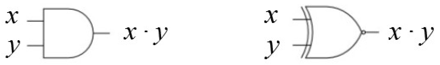
There are four methods that are used to encode numbers in SCo: unsigned classical stochastic encoding (UCSE), signed classical stochastic encoding (SCSE), unsigned extended stochastic encoding (UESE) and signed extended stochastic encoding (SESE) [41,42]. Implementation of different functions strongly depends on the chosen encoding. As an example, when using UCSE, an AND gate is used to implement the product of two inputs, while a XNOR gate performs that operation when using the SCSE encoding, as shown in Figure 1. Moreover, the same logical gate can perform different operations depending on whether the random signals generated are correlated or not. As an example, with USCE encoding, a two-inputs AND gate is used to implement a multiplication for uncorrelated inputs, while it provides the minimum value of the two inputs if they are correlated. In the present work, we will be using SCSE, and, thus, our numbers will lay in the real (−1..1) domain. Thus, multiplication requires the use of an XNOR gate.
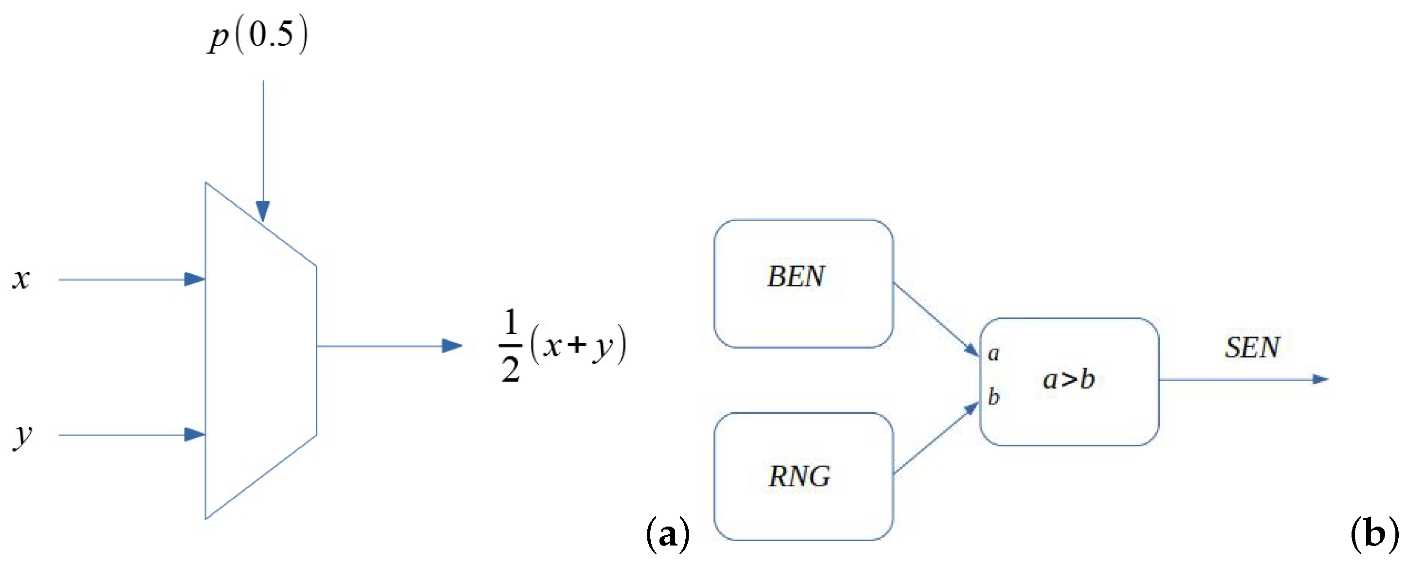
Performing an addition is slightly more complex, because numbers with a probability higher than one cannot be represented, and we may need to add 1 + 1 = 2. Thus, it is better to implement an alternate form as , which at most will output a value of 1. This operation is usually implemented using a multiplexer, as shown in Figure 2a, where the p (0.5) means a signal with a probability of 0.5 to be ‘1’ or ‘0’. This signal can be generated using one of the bits from the RNG, thus needing no additional circuitry. The same gate is used for the (0..1) and the (−1..1) domains.
Other more complex operations (division [23], square roots [23], etc.) may also be found in the literature, but are not presented here for the sake of clarity. Finally, the conversion of a number encoded as a classical number can be translated to a stochastic representation using the schema presented in Figure 2.
3. Memristor Emulator Design
3.1. Theoretical Design
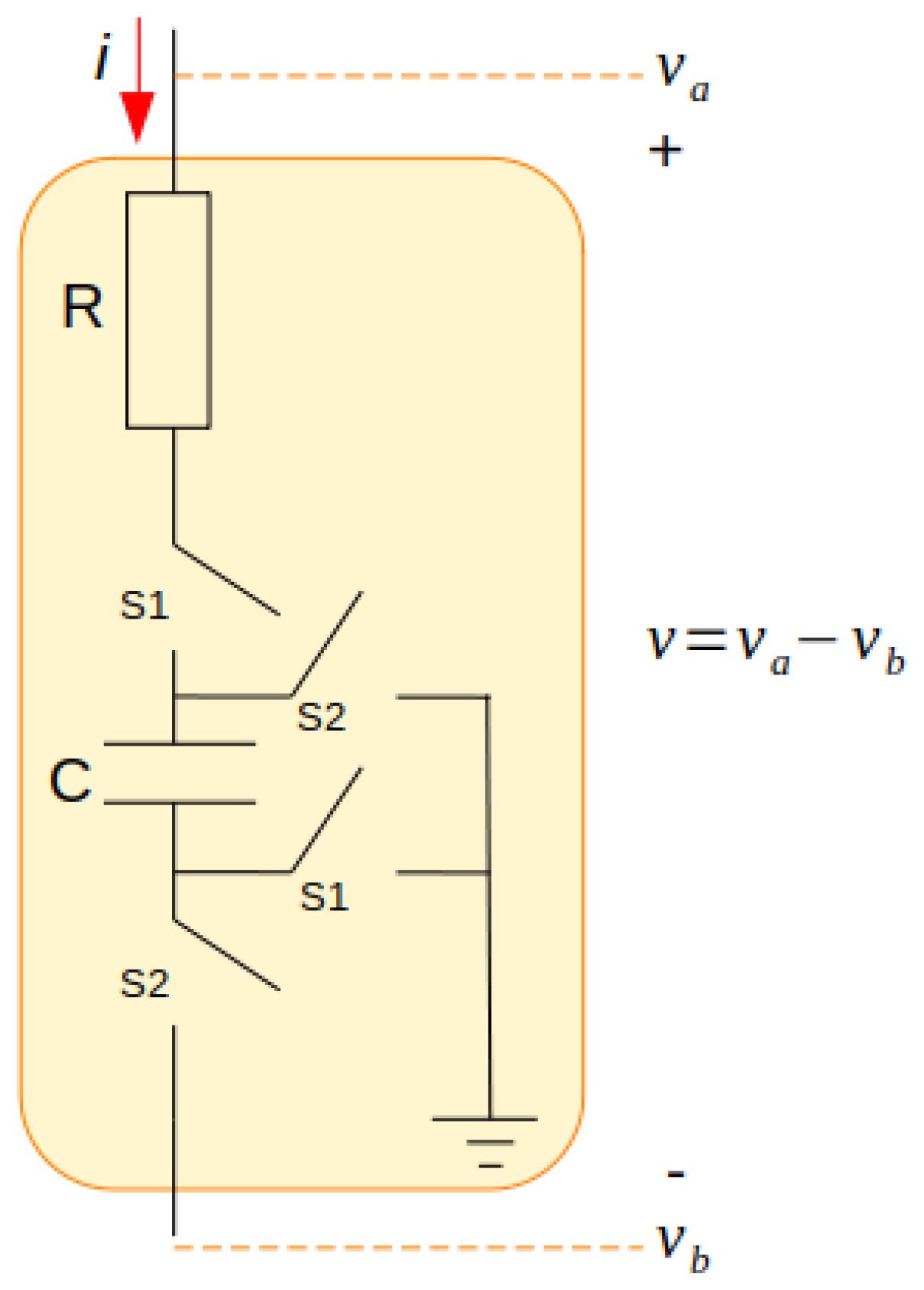
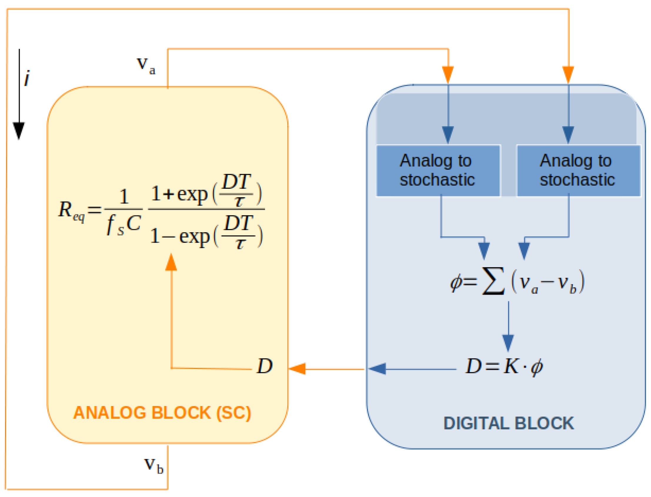
As mentioned above, our system has been implemented in two parts [27,28]. First, we implemented an analog system including the switched capacitor module (SC), as shown in Figure 3, whose equivalent resistance is described by Equation (4). In this case, both control external signals and are equal, with a lag of 180 deg. [43]. The second part is a digital module implementing the control part in stochastic logic, as will be discussed below.
T and are the period and the frequency of the controlling signal and , D is the duty cycle with values between 0 and 1, C is the capacitance value and is the time constant, that is, where C is the capacitor and is the total resistance of the circuit taking into account the parasitic ones.
For our design, in the charge flux domain, it is necessary to calculate the flux from the voltage of the terminals of the SC as a first step. Once this is done, then the relationships between flux and charge are used to obtain the duty cycle (D) that varies the equivalent resistance of the SC. The digital block is the responsible for all these steps.
For this purpose, a series of approximations shall be done to Equation (4). The conductance (G) () can be rewritten as:
where x = DT/.
The use of a first order Taylor expansion of allows us to get a simpler expression. For this, it is necessary to take into account that the decay time of the system is much longer than the control signal period. Thus, we can obtain a simpler equation describing the conductance G:
It is important to notice that this last equation implies that conductance is linearly dependent on the duty cycle D.
To calculate the flux, the digital block converts each voltage terminal of the SC ( and in Figure 3) to non-correlated random values. Then, the corresponding value is accumulated into a counter, which acts as the integrator. Notice that since we are using stochastic computing, this up/down counter needs to count only one up (), one down (), or remain the same (). To implement the memristor device, it is necessary to use an equation to describe the relationship between flux and charge. In this work the simplest relation is used:
where M is a constant. This equation does not include any internal variables. Applying the fourth derivative of the equation, the conductance is:
K is therefore a constant value.
3.2. Simulation Results
In order to be considered as a memristor, the emulator must present two characteristic fingerprints [3,32,33]: (1) a pinched loop (2) whose area changes with frequency.
Figure 6 presents the of the emulator under inputs of different frequency using 16 bits for the stochastic representation. It is apparent from this figure that the curves are pinched at the origin and that the loop area changes with frequency. Thus, we can consider that the two fingerprints are present.
Because of the way it is constructed, the emulator reaches a saturation for the conductance. This is due to the maximum value of , and can be clearly seen at low frequencies, where the maximum value of flux is reached faster. This may also be seen in Figure 7, where the behavior of the Q versus near the origin is quadratic, as can be expected from (7), but it is also seen that its behavior changes to linear after a maximum value for is reached.
It has to be noted that there is a small noise present caused by the stochastic nature of the system, as discussed above. This noise nearly disappears in the saturation, since the counter is practically constant, even though a small ripple is present caused by the stochastic internal behavior. This noise is greatly reduced in the charge and flux domain (Figure 7, because of the integration.
Finally, the current signal for different frequencies is shown in Figure 8. As can be seen there, the maximum conductance (related to the maximum value of the current) is lower for higher values of frequency, as expected.
4. Experimental Implementation
4.1. Experimental Setup
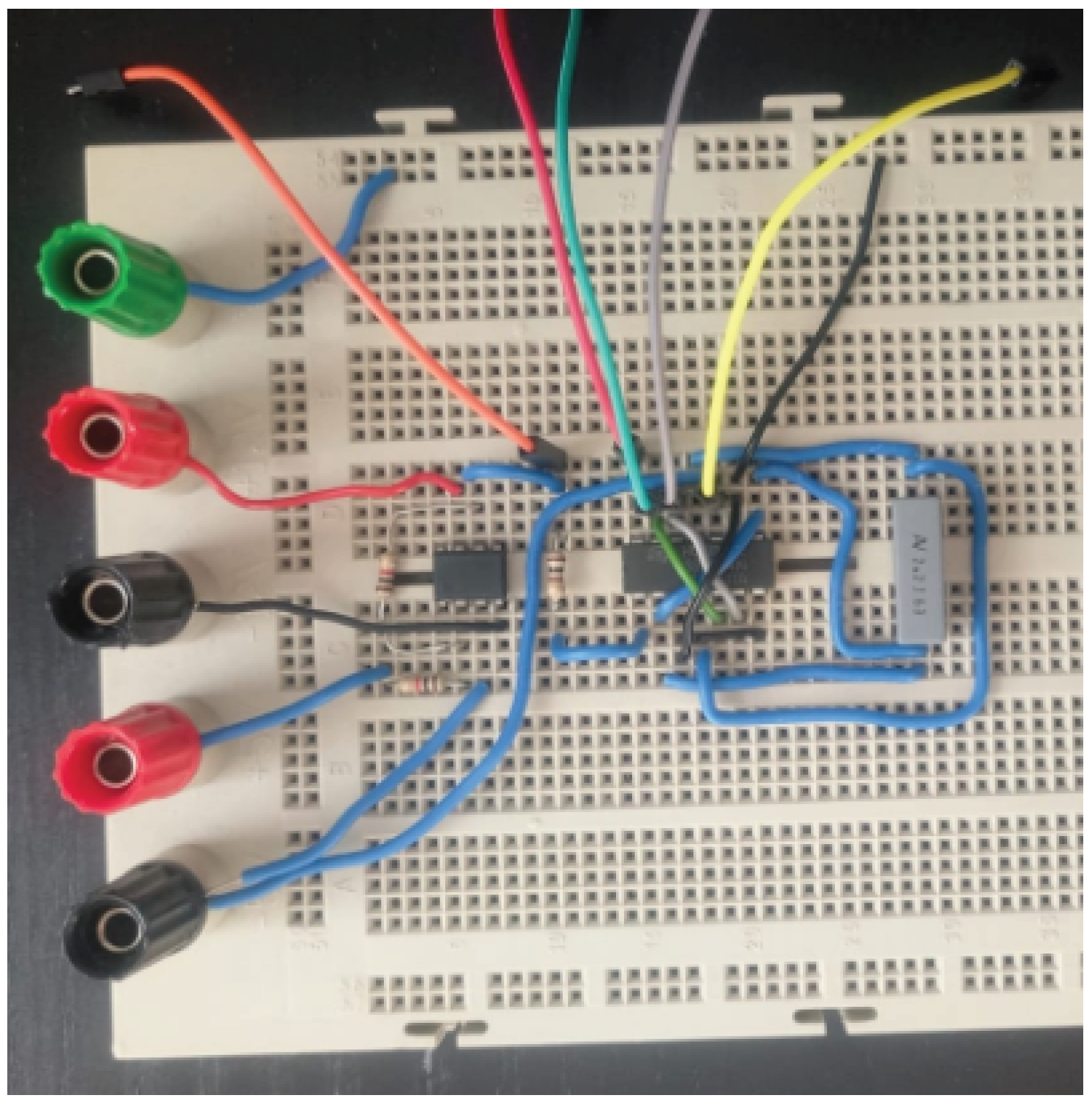
In order to test the proposed circuit, we have implemented a setup similar to that of [28]. We have used a quadruple analog switch HCF4066FE driven by a DE0-Nano FPGA. The analog switch has a working voltage between 0.5 V to 22 V and can switch at a maximum frequency of 25 kHz when the power supply is 3.3 V. The FPGA generated the control signals and using 2 of its 3.3 V digital output pins. Additionally, we have also used a 1 k shunt resistor, along with a 15 F capacitor. The implemented circuit is shown in Figure 9. The conversion from analog to stochastic was performed by first converting from analog to digital using two of the on-board available A/D and then converting this digital value into stochastic, as described above. We have used 16 bits for the stochastic representation, and the needed random numbers were created using a public implementation of the Mersenne twister algorithm [44].
An AFG320 arbitrary signal generator was used to generate the input signal, while two oscilloscopes were used to monitor the full system. An oscilloscope monitored the control signals of the HCF4066FE, while the other oscilloscope was used to monitor the voltage through the shunt resistance of 1 k to obtain the current and also the input voltage, defined as the difference between the two input terminals.
4.2. Experimental Results
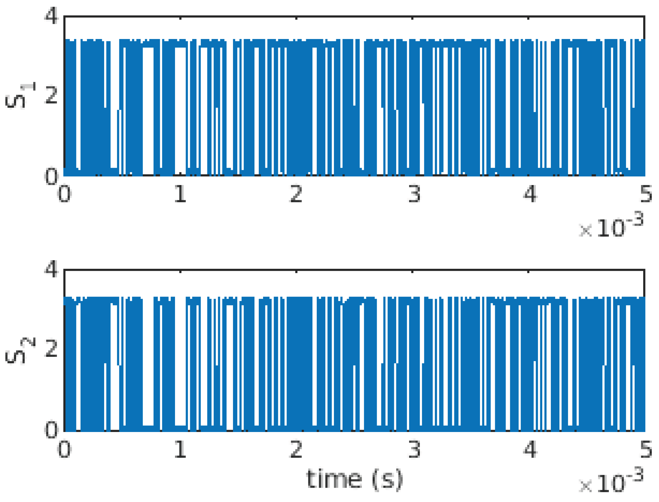
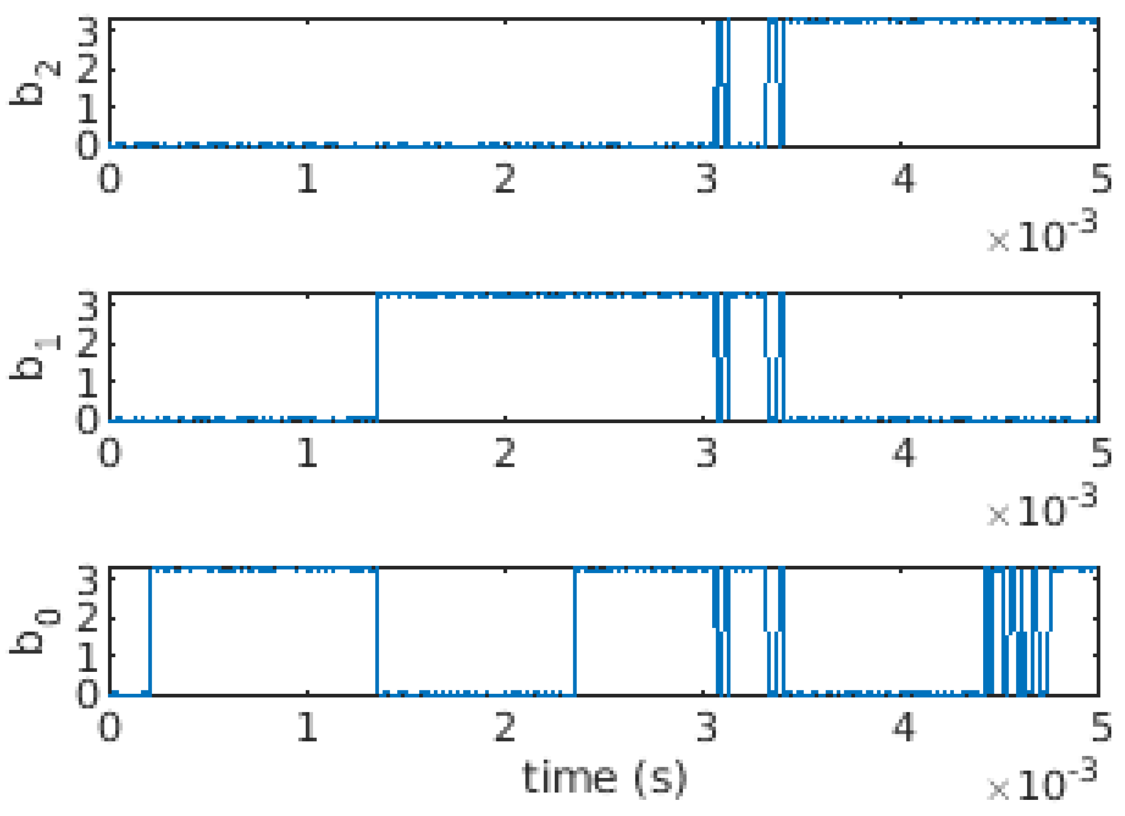
The system has been tested using different input frequencies: 100, 200 and 400 Hz. The internal behaviour of the circuit is depicted in Figure 10 and Figure 11, which depict, respectively, the control signals and in one of these cases and the waveform corresponding to the three least significant bits of the counter.
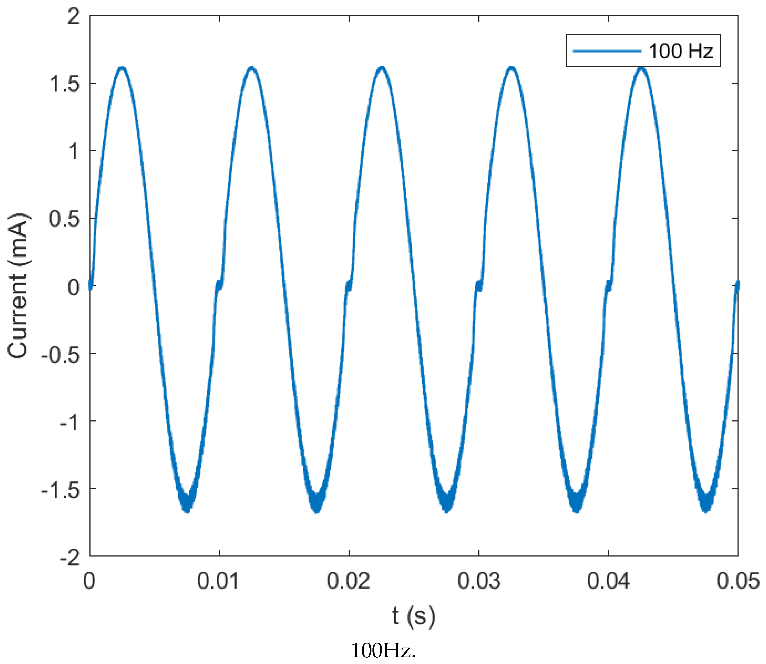
The temporal behavior of the current in these three cases is shown in Figure 12. The currents are clearly nonlinear because of memory: if they were nonlinear due to other effects, then they would be symmetrical, which they are not. In addition, they are showing a dependence on the frequency, as expected for a memristor.
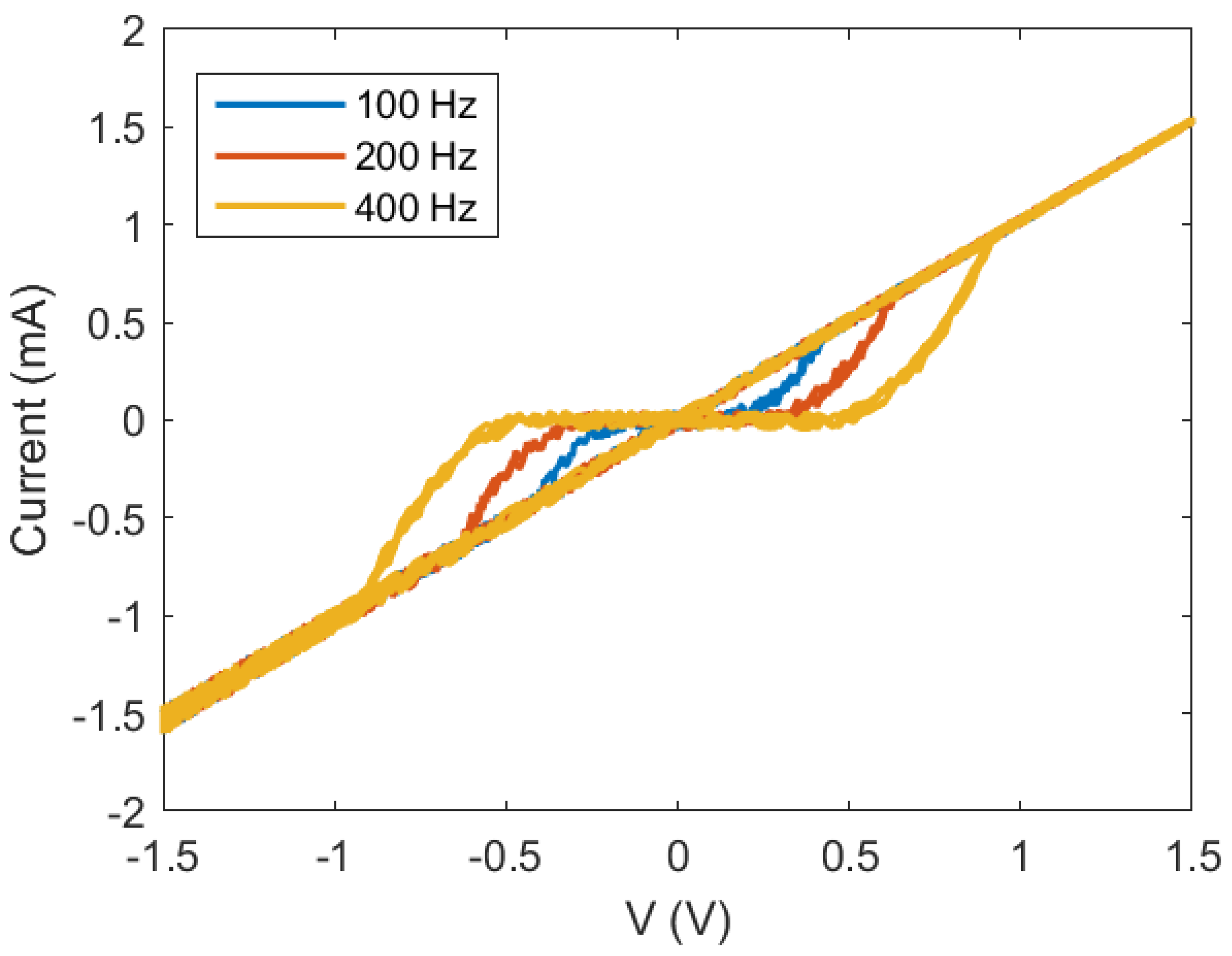
The experimental I-V loops are depicted in Figure 13. On the left figure, the three experimental I-V curves for the corresponding frequencies in Figure 6 (simulations) appear, while the right picture shows an oscilloscope snapshot in the typical case of a 400 Hz driving sine voltage. It is apparent that, in all cases, the experimental fingerprint of a memristor, i.e., the pinched loop [33], is clearly demonstrated. This means that the device has a resistive behavior (it is pinched, which means no current when no voltage is applied), and that this resistance has a memory effect (there is a loop, which means that there are two possible values of the resistance and, hence, the current, for each voltage input value).
Finally, it has to be noted that the area of the loop changes with frequency, with the higher area corresponding to higher frequencies. This is caused by the saturation of the internal counter that corresponds to the flux integral (Equation (3) and Figure 5), which leads to a linear behaviour once the maximum value is reached.
5. Discussion
As discussed above, the design and implementation of memristor emulators is an active research field. In this paper, we have made a contribution to this area by presenting the design, simulation, and experimental implementation of such an emulator. Our proposal is based on using switched capacitors to implement the variable resistor and on using stochastic computing to implement the control part.
The switched capacitor block has been implemented using standard off-the-shelf components with a maximum switching frequency of 25 kHz. The control signals at this frequency are generated inside the control block, which has been implemented into a DE0-nano FPGA. The FPGA reads the analog inputs (the input voltage of the analog block) using its built-in AD converters.
As a first step, we have shown using MATLAB simulation that the design is sound and can implement a system showing the expected fingerprints of a memristor: a closed loop, pinched at the origin. Finally, we have experimentally implemented the design. This actual implementation has been tested using sinusoidal waveforms of different frequencies, and it has behaved as expected. The system shows the memristor fingerprints with noise induced by the switching, as expected.
Thus, the proposed emulator has been shown to perform with its expected behavior, being a promising alternative to be implemented as an IP block into IC designs, since it is a very simple design requiring a lower number of digital gates than similar designs using conventional arithmetic implementations. This implementation would allow the increase of the limiting factor of the switching frequency at 25 kHz caused by the use of a discrete component, and would also proportionally increase the working frequency of the emulator.
Author Contributions
Conceptualization, C.d.B. and R.P.; methodology, C.d.B. and R.P.; software, C.d.B., S.G.S. and R.P.; validation, C.d.B., M.M.A.C. and R.P.; formal analysis, C.d.B. and R.P.; investigation, C.d.B., O.C., M.M.A.C. and R.P.; resources, C.d.B. and R.P.; data curation, C.d.B. and R.P.; writing—original draft preparation, C.d.B., O.C., M.M.A.C., S.G.S. and R.P.; writing—review and editing, C.d.B., O.C., M.M.A.C., S.G.S. and R.P.; visualization, C.d.B., O.C., M.M.A.C. and R.P.; supervision, C.d.B., S.G.S. and R.P.; project administration, C.d.B. and R.P.; funding acquisition, C.d.B. and R.P. All authors have read and agreed to the published version of the manuscript.
Funding
Some of the authors wish to acknowledge support from the DPI2017-86610-P and TEC2017-84877-R projects awarded by the MICINN, as well as the partial support by the FEDER program.
Institutional Review Board Statement
Not applicable.
Informed Consent Statement
Not applicable.
Conflicts of Interest
The authors declare no conflict of interest. The funders had no role in the design of the study; in the collection, analyses, or interpretation of data; in the writing of the manuscript, or in the decision to publish the results.
References
- Chua, L. Memristor-the missing circuit element. IEEE Trans. Circuit Theory 1971, 18, 507–519. [Google Scholar] [CrossRef]
- Strukov, D.B.; Snider, G.S.; Stewart, D.R.; Williams, R.S. The missing memristor found. Nature 2008, 453, 80–83. [Google Scholar] [CrossRef] [PubMed]
- Stavrinides, S.G.; Picos, R.; Corinto, F.; Al Chawa, M.M.; de Benito, C. Implementing memristor emulators in hardware. In Mem-Elements for Neuromorphic Circuits with Artificial Intelligence Applications; Academic Press: Cambridge, MA, USA, 2021; pp. 17–40. [Google Scholar]
- Ascoli, A.; Corinto, F.; Tetzlaff, R. A class of versatile circuits, made up of standard electrical components, are memristors. Int. J. Circuit Theory Appl. 2016, 44, 127–146. [Google Scholar] [CrossRef]
- Kalomiros, J.; Stavrinides, S.G.; Corinto, F. A two-transistor non-ideal memristor emulator. In Proceedings of the Modern Circuits and Systems Technologies (MOCAST), 2016 5th International Conference, Thessaloniki, Greece, 12–14 May 2016; pp. 1–4. [Google Scholar]
- Kim, H.; Sah, M.P.; Yang, C.; Cho, S.; Chua, L.O. Memristor emulator for memristor circuit applications. IEEE Trans. Circ. Syst. I Regul. Pap. 2012, 59, 2422–2431. [Google Scholar]
- Li, Z.; Zeng, Y.; Ma, M. A novel floating memristor emulator with minimal components. Act. Passiv. Electron. Components 2017, 2017, 1609787. [Google Scholar] [CrossRef] [Green Version]
- Vourkas, I.; Abusleme, A.; Ntinas, V.; Sirakoulis, G.C.; Rubio, A. A Digital Memristor Emulator for FPGA-Based Artificial Neural Networks. In Proceedings of the Verification and Security Workshop (IVSW), Sant Feliu de Guixols, Spain, 4–6 July 2016; pp. 1–4. [Google Scholar]
- Ranjan, R.; Ponce, P.M.; Kankuppe, A.; John, B.; Saleh, L.A.; Schroeder, D.; Krautschneider, W.H. Programmable memristor emulator asic for biologically inspired memristive learning. In Proceedings of the Telecommunications and Signal Processing (TSP), 2016 39th International Conference, Vienna, Austria, 27–29 June 2016; pp. 261–264. [Google Scholar]
- Kolka, Z.; Vavra, J.; Biolkova, V.; Ascoli, A.; Tetzlaff, R.; Biolek, D. Programmable Emulator of Genuinely Floating Memristive Switching Devices. In Proceedings of the 2019 26th IEEE International Conference on Electronics, Circuits and Systems (ICECS), Genova, Italy, 27–29 November 2019; pp. 217–220. [Google Scholar]
- Romero, F.J.; Ohata, A.; Toral-Lopez, A.; Godoy, A.; Morales, D.P.; Rodriguez, N. Memcapacitor and Meminductor Circuit Emulators: A Review. Electronics 2021, 10, 1225. [Google Scholar] [CrossRef]
- Von Neumann, J. First draft of a report on the EDVAC. IEEE Ann. Hist. Comput. 1993, 15, 27–75. [Google Scholar] [CrossRef]
- Von Neumann, J. Probabilistic logics and the synthesis of reliable organisms from unreliable components. Autom. Stud. 1956, 34, 43–98. [Google Scholar]
- Von Neumann, J.; Pierce, R.S. Lectures on Probabilistic Logics and the Synthesis of Reliable Organisms from Unreliable Components; California Institute of Technology: Pasadena, CA, USA, 1952. [Google Scholar]
- Gaines, B.R. Stochastic computing. In Proceedings of the Spring Joint Computer Conference, New York, NY, USA, 18–20 April 1967; pp. 149–156. [Google Scholar]
- Poppelbaum, W.; Afuso, C.; Esch, J. Stochastic computing elements and systems. In Proceedings of the Fall Joint Computer Conference, Anaheim, CA, USA, 14–16 November 1967; pp. 635–644. [Google Scholar]
- Fick, D.; Kim, G.; Wang, A.; Blaauw, D.; Sylvester, D. Mixed-signal stochastic computation demonstrated in an image sensor with integrated 2D edge detection and noise filtering. In Proceedings of the IEEE 2014 Custom Integrated Circuits Conference, San Jose, CA, USA, 15–17 September 2014; pp. 1–4. [Google Scholar]
- Camps, O.; Stavrinides, S.G.; Picos, R. Efficient Implementation of Memristor Cellular Nonlinear Networks using Stochastic Computing. In Proceedings of the 2020 European Conference on Circuit Theory and Design (ECCTD), Sofia, Bulgaria, 7–10 September 2020; pp. 1–4. [Google Scholar]
- Camps, O.; al Chawa, M.M.; Stavrinides, S.G.; Picos, R. Stochastic Computing Emulation of Memristor Cellular Nonlinear Networks. 2021; Preprints. [Google Scholar]
- Wang, R.; Han, J.; Cockburn, B.; Elliott, D. Stochastic circuit design and performance evaluation of vector quantization. In Proceedings of the 2015 IEEE 26th International Conference on Application-Specific Systems, Architectures and Processors (ASAP), Toronto, ON, Canada, 27–29 July 2015; pp. 111–115. [Google Scholar]
- Yuan, B.; Wang, Y.; Wang, Z. Area-efficient scaling-free DFT/FFT design using stochastic computing. IEEE Trans. Circ. Syst. II Express Briefs 2016, 63, 1131–1135. [Google Scholar] [CrossRef]
- Camps, O.; Stavrinides, S.G.; Picos, R. Stochastic Computing Implementation of Chaotic Systems. Mathematics 2021, 9, 375. [Google Scholar] [CrossRef]
- Toral, S.; Quero, J.; Franquelo, L.G. Digital stochastic realization of complex analog controllers. IEEE Trans. Ind. Electron. 2002, 49, 1101–1109. [Google Scholar]
- Toral, S.; Quero, J.; Ortega, J.; Franquelo, L. Stochastic A/D sigma-delta converter on FPGA. In Proceedings of the 42nd Midwest Symposium on Circuits and Systems (Cat. No. 99CH36356), Las Cruces, NM, USA, 8–11 August 1999; Volume 1, pp. 35–38. [Google Scholar]
- Toral, S.; Quero, J.; Franquelo, L. Stochastic pulse coded arithmetic. In Proceedings of the 2000 IEEE International Symposium on Circuits and Systems (ISCAS), Geneva, Switzerland, 28–31 May 2000; Volume 1, pp. 599–602. [Google Scholar]
- Moons, B.; Verhelst, M. Energy-efficiency and accuracy of stochastic computing circuits in emerging technologies. IEEE J. Emerg. Sel. Top. Circ. Syst. 2014, 4, 475–486. [Google Scholar] [CrossRef]
- De Benito, C.; Camps, O.; Al Chawa, M.; Stavrinides, S.; Picos, R. A Stochastic Switched Capacitor Memristor Emulator. In Proceedings of the 2021 10th International Conference on Modern Circuits and Systems Technologies (MOCAST), Thessaloniki, Greece, 5–7 July 2021; pp. 1–4. [Google Scholar]
- Svetoslavov, G.; Camps, O.; Stavrinides, S.G.; Picos, R. A Switched Capacitor Memristive Emulator. IEEE Trans. Circ. Syst. II Express Briefs 2020, 68, 1463–1466. [Google Scholar] [CrossRef]
- Chua, L.O.; Kang, S.M. Memristive devices and systems. Proc. IEEE 1976, 64, 209–223. [Google Scholar] [CrossRef]
- Leon, C. Everything you wish to know about memristors but are afraid to ask. Radioengineering 2015, 24, 319. [Google Scholar]
- Corinto, F.; Civalleri, P.P.; Chua, L.O. A theoretical approach to memristor devices. IEEE J. Emerg. Sel. Top. Circ. Syst. 2015, 5, 123–132. [Google Scholar] [CrossRef] [Green Version]
- Biolek, D.; Biolek, Z.; Biolková, V.; Kolka, Z. Some fingerprints of ideal memristors. In Proceedings of the Circuits and Systems (ISCAS), 2013 IEEE International Symposium, Beijing, China, 19–23 May 2013; pp. 201–204. [Google Scholar]
- Chua, L. If it’s pinched it’s a memristor. Semicond. Sci. Technol. 2014, 29, 104001. [Google Scholar] [CrossRef]
- Ielmini, D.; Milo, V. Physics-based modeling approaches of resistive switching devices for memory and in-memory computing applications. J. Comput. Electron. 2017, 16, 1121–1143. [Google Scholar] [CrossRef] [Green Version]
- Chang, K.C.; Chang, T.C.; Tsai, T.M.; Zhang, R.; Hung, Y.C.; Syu, Y.E.; Chang, Y.F.; Chen, M.C.; Chu, T.J.; Chen, H.L.; et al. Physical and chemical mechanisms in oxide-based resistance random access memory. Nanoscale Res. Lett. 2015, 10, 120. [Google Scholar] [CrossRef] [Green Version]
- Williams, R.S.; Pickett, M.D.; Strachan, J.P. Physics-based memristor models. In Proceedings of the Circuits and Systems (ISCAS), 2013 IEEE International Symposium, Beijing, China, 19–23 May 2013; pp. 217–220. [Google Scholar]
- Chen, T.H.; Hayes, J.P. Design of Division Circuits for Stochastic Computing. In Proceedings of the 2016 IEEE Computer Society Annual Symposium on VLSI (ISVLSI), Pittsburgh, PA, USA, 11–13 July 2016; pp. 116–121. [Google Scholar]
- Mitra, S.; Banerjee, D.; Naskar, M.K. A Low Latency Stochastic Square Root Circuit. In Proceedings of the 2021 34th International Conference on VLSI Design and 2021 20th International Conference on Embedded Systems (VLSID), Virtual Event, 20–24 February 2021; pp. 7–12. [Google Scholar]
- Wu, D.; Miguel, J.S. In-Stream Stochastic Division and Square Root via Correlation. In Proceedings of the 2019 56th ACM/IEEE Design Automation Conference (DAC), Las Vegas, NV, USA, 2–6 June 2019; pp. 1–6. [Google Scholar]
- Qin, Z.; Qiu, Y.; Zheng, M.; Dong, H.; Lu, Z.; Wang, Z.; Pan, H. A universal approximation method and optimized hardware architectures for arithmetic functions based on stochastic computing. IEEE Access 2020, 8, 46229–46241. [Google Scholar] [CrossRef]
- Gaines, B.R. R68-18 random pulse machines. IEEE Trans. Comput. 1968, 100, 410. [Google Scholar] [CrossRef]
- Gaines, B.R. Stochastic computing systems. In Advances in Information Systems Science; Springer: Berlin/Heidelberg, Germany, 1969; pp. 37–172. [Google Scholar]
- Kimball, J.W.; Krein, P.T.; Cahill, K.R. Modeling of capacitor impedance in switching converters. IEEE Power Electron. Lett. 2005, 3, 136–140. [Google Scholar] [CrossRef]
- Forencich, A. Verilog Implementation of Mersenne Twister PRNG. 2018. Available online: https://github.com/alexforencich/verilog-mersenne (accessed on 15 February 2020).
Figure 1.
Basic implementation scheme of a SC multiplier in the (0..1) range (AND gate, left) and in the (−1..1) range (XNOR gate, right).
Figure 1.
Basic implementation scheme of a SC multiplier in the (0..1) range (AND gate, left) and in the (−1..1) range (XNOR gate, right).

Figure 2.
Basic implementation schemes (a) of a SC adder using a multiplexer and (b) a stochastic number generator (SGN) which converts a binary encoded number (BEN) to a stochastic encoded number (SEN) using a random number generator (RNG).
Figure 2.
Basic implementation schemes (a) of a SC adder using a multiplexer and (b) a stochastic number generator (SGN) which converts a binary encoded number (BEN) to a stochastic encoded number (SEN) using a random number generator (RNG).

Figure 3.
Switched capacitor (SC) circuit schematic.

Figure 4.
Swiched capacitor memristor emulator (SCME) block diagram.

Figure 5.
Control block implementation using stochastic computing.

Figure 6.
Simulated characteristic curves of the memristor implemented using Figure 4. Three different frequencies are shown in different colors.
Figure 6.
Simulated characteristic curves of the memristor implemented using Figure 4. Three different frequencies are shown in different colors.

Figure 7.
characteristics of the memristor implemented using Figure 4. The different frequencies (in arbitrary units) are shown in different colors.
Figure 7.
characteristics of the memristor implemented using Figure 4. The different frequencies (in arbitrary units) are shown in different colors.

Figure 8.
Current signal (response) for different frequencies, as obtained from the simulation. The three different frequencies are shown in different colors and correspond to the ones shown in Figure 6.
Figure 8.
Current signal (response) for different frequencies, as obtained from the simulation. The three different frequencies are shown in different colors and correspond to the ones shown in Figure 6.

Figure 9.
Physical implementation of the circuit on a prototyping board.

Figure 10.
Stochastic signals and generated by the control circuit.

Figure 11.
Three least significant bits of the counter ( is the least significant bit) at a specific time.
Figure 11.
Three least significant bits of the counter ( is the least significant bit) at a specific time.

Figure 12.
Temporal graphs of the measured response (current signals) of the realized memristor at 3 different frequencies corresponding to the simulated frequencies for driving sine voltage of (a) 100 Hz, (b) 200 Hz, and (c) 400 Hz.
Figure 12.
Temporal graphs of the measured response (current signals) of the realized memristor at 3 different frequencies corresponding to the simulated frequencies for driving sine voltage of (a) 100 Hz, (b) 200 Hz, and (c) 400 Hz.


Figure 13.
Measured I-V signals at different frequencies.

Publisher’s Note: MDPI stays neutral with regard to jurisdictional claims in published maps and institutional affiliations. |
© 2022 by the authors. Licensee MDPI, Basel, Switzerland. This article is an open access article distributed under the terms and conditions of the Creative Commons Attribution (CC BY) license (https://creativecommons.org/licenses/by/4.0/).
Share and Cite
MDPI and ACS Style
de Benito, C.; Camps, O.; Al Chawa, M.M.; Stavrinides, S.G.; Picos, R. A Switched Capacitor Memristor Emulator Using Stochastic Computing. Technologies 2022, 10, 39. https://0-doi-org.brum.beds.ac.uk/10.3390/technologies10020039
AMA Style
de Benito C, Camps O, Al Chawa MM, Stavrinides SG, Picos R. A Switched Capacitor Memristor Emulator Using Stochastic Computing. Technologies. 2022; 10(2):39. https://0-doi-org.brum.beds.ac.uk/10.3390/technologies10020039
Chicago/Turabian Stylede Benito, Carola, Oscar Camps, Mohamad Moner Al Chawa, Stavros G. Stavrinides, and Rodrigo Picos. 2022. "A Switched Capacitor Memristor Emulator Using Stochastic Computing" Technologies 10, no. 2: 39. https://0-doi-org.brum.beds.ac.uk/10.3390/technologies10020039
Note that from the first issue of 2016, this journal uses article numbers instead of page numbers. See further details here.