Article

Miniaturized Microstrip Dual-Channel Diplexer Based on Modified Meander Line Resonators for Wireless and Computer Communication Technologies

by
Yaqeen Sabah Mezaal
1,*,
Shahad K. Khaleel
2,
Ban M. Alameri
3,4,
Kadhum Al-Majdi
5 and
Aqeel A. Al-Hilali
6
1
Mobile communication and Computing Engineering, University of Information Technology and Communications, Baghdad 10068, Iraq
2
Technical Electronic Department, Technical Instructors Training Institute, Middle Technical University, Baghdad 10074, Iraq
3
Department of Electrical Engineering, Faculty of Engineering, Mustansiriyah University, Baghdad 10047, Iraq
4
School of Telecommunication Engineering, University of Malaga, 29010 Malaga, Spain
5
Medical Instrumentation Engineering Department, Ashur University, Baghdad 10047, Iraq
6
Medical Instrumentation Engineering Department, Al-Farahidi University, Baghdad 10070, Iraq
*
Author to whom correspondence should be addressed.
Submission received: 1 March 2024 / Revised: 17 April 2024 / Accepted: 19 April 2024 / Published: 24 April 2024

Abstract

:
There has been a lot of interest in microstrip diplexers lately due to their potential use in numerous wireless and computer communication technologies, including radio broadcasts, mobile phones, broadband wireless, and satellite-based communication systems. It can do this because it has a communication channel that can combine two distinct filters into one. This article presents a narrow-band microstrip diplexer that uses a stepped impedance resonator, a uniform impedance resonator, tiny square patches, and a meander line resonator. The projected diplexer might be made smaller than its initial dimensions by utilizing the winding construction. To model the microstrip diplexer topology for WiMAX and WIFI/WLAN at 1.66 GHz and 2.52 GHz, the Advanced Wave Research (AWR) solver was employed. It exhibited an insertion loss of 3.2 dB and a return loss of 16 dB for the first channel, while the insertion loss and return loss were 2.88 dB and 21 dB, respectively, for the second channel. When both filters were simulated, the band isolation was 31 dB. The projected microstrip diplexer has been fabricated using an FR4 epoxy laminate with dimensions of 32 × 26 mm2. The simulated S-parameters phase and group delay closely matched the measurements.

1. Introduction

Modern wireless and computer communication technologies, such as satellites, mobile communications, and radar, heavily rely on microwave filters to ensure the required frequency selectivity. Effective signal management across diverse frequency bands is made possible by diplexers and multiplexers, which are key components in these systems. Passive multiplexers utilize multiple filters and a shared junction to combine or separate signals from different frequency bands. Over the past few years, diplexers have gained significant importance in various wireless communication systems, including mobile phone networks, satellite communication, broadband wireless communication, broadcasting, and terrestrial communication [1,2,3,4]. Diplexers accomplish this by combining two distinct filters into one unit, taking advantage of communication channels. As an example, a microwave diplexer enables two filters to utilize a single antenna while reducing interference between the signals, as illustrated in Figure 1. Through the utilization of a single antenna, this overall reduction in weight and size of the device is achieved through the consolidation of filters and signals. A great number of advancements in diplexer and multiplexer technologies have been made possible as a result of the progression of standards. To be more specific, a diplexer is utilized to transform two antennas that operate on distinct frequencies into a single port that is shared by both of them [5,6,7,8].

2. State of the Art

With the debut of the antenna in the 1970s, the concept of the microstrip antenna was initially established for the first time. An increase in the number of study articles has been written about the concept by several researchers from different countries [8,9,10]. The development of innovative designs for microstrip antennas has been prompted by the rise in the number of applications that make use of wireless communication. The objective of these designs is to attain a high level of performance in modern communication systems. The filters and diplexers are components that are utilized in modern communication systems, and each of these components performs substantial and equally vital duties. A well-designed diplexer should not only be priced reasonably, but it should also be very effective in terms of performance. All of these qualities should be present. In the conventional method of manufacturing microstrip diplexers, the operations of first making two separate filters and then constructing a matching circuit are carried out. This is the standard way. The easiest approach is to make use of a combination of two band-pass filters (BPFs), as stated in reference [11,12,13,14]. As a result of their architectural design, microstrip diplexers are designed to be utilized in a wide number of applications that involve wireless communication. During the process of designing and creating the diplexer, several potential structures have been proposed.
When it comes to RF diplexers constructed based on diverse filter designs [15], there are a few different approaches that may be applied; however, the three methods that are listed below are the ones that are utilized the most frequently:
One of the first strategies is the utilization of two BPFs, each of which has a center frequency that is distinct from the other. The employment of a bandpass filter for one channel and a bandstop filter for the other channel, both of which are designed to reject the same frequency band, is another instance of this. The interaction between these filters when employed together is important. For example, using two band-stop filters, each with a different center frequency, may be essential in certain instances.
Each diplexer is equipped with two channels, and each of these channels runs at a different frequency to accommodate a certain group of applications. To give you an example, the authors of the reported paper in [16], introduced a diplexer that was developed specifically for WiMAX wireless communications. Instead, the authors of [17] came up with the idea for a diplexer during the same year. Both GSM-4G and frequency division duplex applications were taken into consideration during the development of this diplexer.
A microstrip diplexer filter with good isolation has been reported in [18]. The short stubs-load resonator technique, upon which this filter was built, is based on a feeding line coupling approach. The building of this filter was made possible utilizing this method. Specifically, the filter was made to provide transmission zero at a lower frequency than the original frequency. Its primary aim during development was to meet the needs of wireless communications requiring an exceptionally high degree of isolation. It is designed for use in those areas and features two channels that operate at 3 and 5 GHz.
In 2019, a small microstrip diplexer built on a dual closed-loop stepped impedance resonator (DCLSIR) was described by the authors of [19]. The DCLSIR stands for the building block of this diplexer. The necessary properties of the microstrip diplexer can be achieved by merging two DCLSIR-BPFs to be operated at 8.3/10 GHz.
To create a new structure for design purposes, the authors of [20] proposed the idea of a planar dual-channel microstrip BPF in 2020. Given that the suggested diplexer has large fractional bandwidths (FBWs %) of 34.3% for the first channel and 38.6% for the second channel. It could be used in broadband applications. For that reason, it is suitable for use in applications that necessitate broadband speeds. In contrast to the 1.6 GHz used by L-band, the WiMAX resonant frequency is 3 GHz.
The microstrip diplexer was developed to be utilized in GSM applications. Before it was put into operation, this diplexer was supposed to operate at frequencies of 0.78 GHz and 1.85 GHz, respectively [21]. The thin cells and patch served as the design keywords of this device. Because the resonator that has been proposed has a symmetrical construction, research into both the odd and even modes must be undertaken to gather knowledge concerning the resonator behavior. The diplexer has provided high levels of isolation, low levels of insertion losses, and very good return losses.
An innovative compacted substrate integrated waveguide (SIW) diplexer with square cavities was proposed in [22] for C-band application. This diplexer operates at a frequency that is lower than the cutoff frequency that is determined by the cavity. It is responsible for applying the evanescent-mode propagation mechanism so that it can transmit signals. When the center frequency is adjusted to 6.16 GHz and 7.72 GHz, respectively, insertion losses of 0.83 dB and 0.77 dB are detected in the lower and higher passbands. These frequencies correspond to the lower and higher passbands, respectively. About 5.1% fractional bandwidth is provided for every passband provided by the diplexer that has been presented regardless of the passband. In addition to that, it provides an isolation level of 22 dB.
In [23], the authors have developed a microstrip diplexer that is not only extremely isolated but also extremely small in terms of the electrical components that it contains. Specifically, this specific diplexer is intended to be utilized in the Radio Occultation (RO) System. It is utilized in a significant manner to investigate a wide range of properties that are associated with the atmospheres of planetary systems. Many of these features are the subject of ongoing research. Research on planetary atmospheric properties is currently underway using the radio occultation technique. The onboard RO transmitter depends on the frequency synthesizers to ensure its proper functioning. This transmitter operates in two distinct frequency bands, with one at 6.7 GHz and the other at 8.4 GHz.
A miniature narrow-band microstrip diplexer with two channels has been perceived in [24] using an FR4 substrate. Two bandpass filters, each operating in a specific frequency range, connect at a single junction to create it. The standard components of every BPF include input and output feedlines, a resonator with meandering lines, a step impedance resonator (SIR), and a uniform impedance resonator (UIR).
In a recent study, an artificial neural network (ANN) was utilized to aid in the build-up and design of a high-performance microstrip diplexer [25]. An ANN model takes into account various factors. These factors to consider are the input frequency, substrate type, substrate thickness, and physical dimensions. Another output from this model is the generation of group delay values (GD), along with S-parameters. Neural networks trained via back propagation usually function within a frequency range of 1.4 to 3 GHz.
To construct multifunction integrated diplexers that are capable of carrying out operations such as frequency selection, frequency division, and power division, the paper reported in [26] came up with an innovative circuit model. This unique circuit model was developed to develop multifunction integrated diplexers. The highly integrated multifunctional diplexer that has been presented is composed of dual simple multimode resonators that operate at distinct frequencies, in addition to dual isolation resistors. This diplexer is designed to perform multiple functions simultaneously for integrating the two multimode resonators based on the distributed coupling method. The responses have shown both the second- and third-level order. Both of these orders have been given consideration.
A dual-channel diplexer using linked open-loop microstrip resonators is proposed and investigated in the article [27] using an ADS simulator. Simulated results for this device indicate insertion loss values of 1.8 and 1.0 dB at 1st and 2nd loads, respectively. With the use of microstrip open-loop resonators and source-load coupling lines, 35 dB-isolated channel bands have been efficiently created. In article [28], the researchers have a definition for diplexers, which are dual-filter circuits with three ports, that allow for the simultaneous use of an antenna by two separate frequency channels. However, this technology can be used with several transmitters operating at different frequencies as long as each band is used for sending and receiving signals. SIR combined with UIR provides all the benefits of fractal filters with much simpler modeling and manufacturing requirements. Kappa substrate, which has a very low loss tangent value, can be employed in diplexer, triplexer, and quadruplexer components.
This research paper describes an investigation of a highly narrowband microstrip diplexer that makes use of meander line resonators, tiny square patches, UIR, and SIR. An investigation into this diplexer was the purpose of the study that was carried out. In addition to having low profile topologies, and compact dimensions, efficient band isolation of 31 dB between frequency channels has been obtained.

3. Design

To keep up with the ever-increasing complexity of these systems, engineers have been coming up with more creative and intricate designs. This is because diplexers are so integral to contemporary communication systems. There are specific requirements that diplexers must meet to be employed in multi-service and multi-band communications. Conversely, larger and more complex diplexers were produced by the conventional way of fabrication, which required a great number of external connectors [26,27,28,29,30]. This has led to the development of numerous different designs that can guarantee compliance with these regulations. Diplexers have an assortment of resonators, including meander lines, open-loop resonators, stepped impedance resonators (SIRs), spiral inductor resonators, and many more. This has been done to achieve both good performance and a reduction in the size of the circuit. Basically, the resonator is capable of storing electromagnetic energies under particular frequencies in L and C elements. Magnetic energy is stored in the inductor L, whereas electric energy is stored in the capacitor C.
The construction of SIRs involves the utilization of a network of transmission lines that are interconnected with one another. Each transmission line is created with its specific impedance requirement. SIRs are frequently utilized in a wide variety of applications within the realm of radio frequency (RF) and microwave engineering. As a result of their diminutive size and remarkable Q-factor, they are very well-suited for use in oscillators and filters. They are incredibly beneficial for a wide variety of applications due to the extraordinary properties that they possess, which is the reason why this is the case. During the process of developing SIRs, design issues and the undesirable reactions of particular circuits were also taken into account by RF and microwave engineers. The development of SIRs was motivated by these limits. While lower SIRs can limit frequencies up to a certain point, larger UIRs are more commonly seen in RF and microwave devices. A wide range of additional uses also make use of UIRs. Figure 2 and Figure 3 display multiple examples of feasible SIR designs. There is a physical difference between the SIR and UIR lines; the former is shorter [30]. This holds even though UIR and SIR are based on ABCD matrices. One possible approach to express the matrix is as follows:
A B C D = C o s   θ j   Z 0   S i n   θ j   Z 0 1 S i n   θ C o s   θ
Alternatively, Z 0 is used to represent characteristic impedance and θ is used to represent the length of the UIR line. There are more design options available in the SIR topology than in topologies that use uniform impedance resonators because it permits the insertion of three matrices at each node instead of the matrix. The reason behind this is that three matrices can be introduced into the system using the SIR topology. This matrix is an effective tool for SIR topologies to improve their overall performance. On the other hand, UIR topologies do not depend on anything other than line length to produce resonance. In SIRs, the resonance state is strongly affected by the length and impedance ratios that are considered. To fully comprehend the operation of SIRs in UIR structures, which are commonly used to build microwave filters, these characteristics are crucial.
Regarding this specific case, the impedance ratio coefficient, denoted by K, is equal to Z2/Z1. In contrast, the electrical lengths in the SIR are denoted by the symbols θ1 and θ2. When the value of K is midway between 0 and 1, the electrical length of a resonator is known to be the shortest, and when the value of K is greater than 1, the electrical length is known to be the longest. The presence of a considerable discontinuity in the SIR is discovered for an exceptionally big Z, which results in a low insertion loss [1,30].
According to Figure 3, there are two distinct forms of SIRs, which are referred to as symmetric (SSIR) structures and asymmetrical (ASIR) structures, respectively. Both of these structures are referred to as SIRs. It is a well-known fact that, among the microstrip sections that are utilized in SIR structures, the microstrip segment that has a narrower width possesses a higher impedance in contrast to the microstrip section that has a wider width. It is possible to observe symmetric SIR in situations where the value of Z1 is lower than Z2, and when the value of Z4 is higher than Z5. The values of d1 and d2 are the symbols that are used to represent electrical lengths in symmetrical SIR, while e1 and e2 are used in asymmetrical SIR. A symmetrical SIR shows that the lengths are the same, which is the reason for this difference. In general, symmetrical SIR features end-to-end impedance symmetry in addition to three-step impedance sections. These sections are also characterized by their electrical length. When it comes to the symmetrical SIR, the impedance ratio acts as a replacement for the dimensions condition (K) that is associated with the SIR.
The SIR arrangement makes use of both odd and even excitation to ensure that it processes electrical signals correctly. When the value of Yin is equal to zero, it is possible to observe the resonances that are produced by odd-even excitations with a reasonable amount of ease [31].
It is possible to examine the SIR configuration and this can be accomplished with the assistance of odd and even excitations. It is possible to obtain the consequent resonant frequencies for odd and even excitations by using the condition Yin = 0, as stated in reference [31]. As a result of the condition, these frequencies have been extracted directly.
(a) Odd-mode resonance condition:
t a n   θ 0   t a n   θ s = R  
(b) Even-mode resonance condition:
1 2 R 1   1 + G 2 R G 0 R 1 + G 1 R 2 + G 3 + G 4 R 1 R 1 + G 5 R 2 = 0
The following factors are taken into consideration when determining the parameters:
R = Z0/Zs, R1 = Z1/Zs, R2 = Z2/Zs, G0 =   t a n   θ 1 , G1 =   t a n   θ 2 , G2 =   t a n   θ 0   t a n   θ 1 , G3 =   t a n   θ s , G4 =   t a n   θ 0 , G5 =   t a n   θ 1   t a n   θ 2 .
Figure 4 and Equations (2) and (3) are used to predict the resonance (Fr) for odd mode and even mode, respectively, using Equations (4) and (5).
Fr G 4 + G 3 R 1 π   Z s   R + G 3   G 4 π   Z s   R 2 = 0
Fr 2 R 1 G 5 R 2 1 R 1 1 R G 0 G 3 + G 0 R 1 + G 1 R 2 G 3 + R G 4 + 1 2 π   Z s   G 0 R 1 + G 1 R 2 G 3 G 4 R 1 + R 1 π   Z s   G 5 R 2 1 R 1 G 3 + G 4 R = 0
Figure 5 depicts the lumped element circuit that corresponds to a resonant frequency [32], which can be used to analyze the SIRs.
When it comes to planner layouts, meander line resonators are a representation of easily fabricable formats. The resonators in question are primarily utilized as compactness tools, and they are well-known for the great qualities and compact size that they possess. Figure 6 illustrates the outcomes of their implementation in an LC lumped element circuit, which has resulted in their extensive application [1].
Given the information presented in Figure 6b, the impedance of the LC series can be represented using the equation j(ωL − 1/ωC). Therefore, at the terminal of the meander line resonator, the resistance load can be observed. The phase delay can be described by the following equation:
  Δ θ = t a n 1     ω L 1 ω C R L
A phase constant can be possessed by the meander line resonator, and it is as follows:
β = 2 π λ i
where the symbol λi represents the wavelength of the resonator. By the equations that came before it, the next equation can be expressed as follows:
Δθ = β l
Or
l = Δ θ / β = λ i 2 π   t a n 1     ω L 1 ω C R L
Therefore, Equations (8) and (9) might be taken into consideration within the process of designing this resonator. As shown in Figure 6, the BPF can be constructed by utilizing a series connection between the C and L terminals. This will make it possible to construct the microstrip BPF in accordance with Equation (9). All of the suggested diplexer filters are listed in Table 1, which contains their varied specs.
To design and simulate the microstrip diplexer that was suggested, the AWR program was utilized. This was done to accomplish the aforementioned goals. The diplexer was initially designed to have total substrate dimensions of 32 × 26 mm2, based on FR4 substrate. The microstrip diplexer has a Chebyshev response based on frequency responses received by the AWR simulator. Each filter for the projected microstrip diplexer has only one resonator and can be considered a first-order filter. Meander line resonators, patches, SIR, and UIR components are utilized in the construction of the suggested diplexer, which is illustrated in Figure 7. Intended to improve band isolation and achieve satisfactory frequency responses, the diplexer was projected to operate under frequency channels of 1.66 and 2.52 GHz. The meander line resonator and SIR are two common types of resonators used in microwave and RF filter designs. The meander line has a serpentine-shaped topology, which can create resonance through induction and capacitance without the use of other stubs, perfect for impedance matching. Such an arrangement enhances compactness and it is very easy to be integrated into stripline or microstrip circuits. On the other hand, SIR, which consists of branched line sections taking different characteristic impedances connected in a series, aims to use resistance mismatch at junctions to achieve the impedance. SIR is known to enable the achievement of narrow bands, or harmonics blocking, or sharp transitions between passbands and stopbands, which can also include stubs or tuning elements to be able to adjust a certain band. In the present study, design nullification of stubs in the meander line, as opposed to the SIR, suggests a structural deviation in addition to varying operational principles. This also implies that the frequency responses demanded and the suitability of the SIR and the meander line are structured in qualitatively different ways, for a wide range of microwave and RF applications.
Nearby SMA connectors and the highest points of input/output feeds, a substantial number of SIR elements are located. As a consequence of this, it is essential to implement suitable optimization strategies for each component that is a part of the circuit. Many parameters can affect the resonant frequency of the filter. These factors include the length of the filter, the turn number of meander line resonators, patches, and the existence of both UIR and SIR elements. As may be seen in Figure 7, the dimensions of the diplexer are expressed in millimeters.

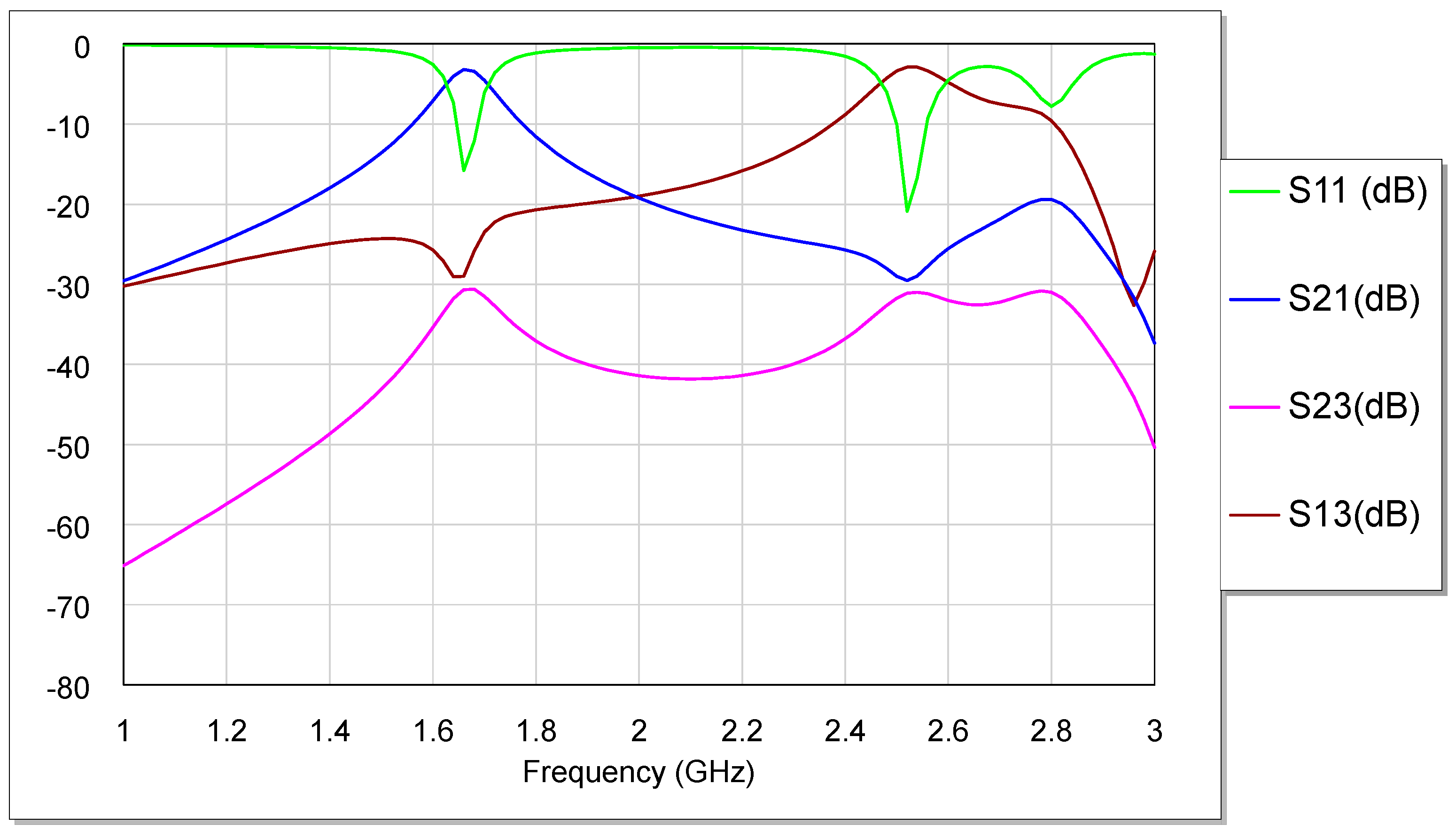
4. Results and Discussion

Figure 8 shows the frequency responses of the proposed microstrip diplexer. At 1.66 GHz for the first channel (Tx), the proposed diplexer design displays an insertion loss (IL) of 3.2 dB and a return loss (RL) of 16 dB. The first frequency band’s transmission channel (Tx) has a fractional bandwidth (∆F) of 4.94% and extends from 1.626 GHz to 1.708 GHz. The reception channel (Rx) for the second frequency band spans the range of 2.469 GHz to 2.598 GHz, with a central frequency of 2.52 GHz and ∆F of 5.12%. Furthermore, the insertion loss and return loss for this channel are detected to be 2.88 dB and 21 dB, respectively. Based on the results of the simulation, it has been determined that the configuration that has been proposed can maintain an isolation of 31 dB between the two filters.
There are some operational characteristics of the diplexer that are depicted in Figure 9. A few examples of these features are the scattering parameters’ group delays (S11, S21, S31, and S32). A visual representation of these qualities can be found in the figure and Table 2. It is necessary to make use of the group delay (GD) measurement to acquire an understanding of the average filter delay over a variety of frequencies. A negative group delay indicates that the diplexer can forecast the position of the pulse at a later time by making use of the current location of the pulse rather than the position of the pulse at the time of prediction. It is possible to conclude that a negative group delay is a signal delay and is an essential property that must be taken into consideration when developing a diplexer. This conclusion can be reached following the aforementioned information. In the realm of radio frequency microwave systems, it has garnered a significant amount of attention in recent years. Below, you can find a detailed table that describes each value contributing to the group delay. Operation of a microstrip diplexer with a negative group delay requires the use of the phase of some special components like meander line resonators as a source of the required phase shift. Additionally, it clocks signals and performs such functions as signal processing, filtering, and equalization to eventually improve performance of high-tech communication systems through the reduction of latency and the gaining of greater transmission rates. A good design and appropriate tuning should be achieved in order to meet the negative group delay needs for special application function.
One of the most fundamental capabilities that may be found in a variety of devices, such as diplexers, amplifiers, and filters, is the capacity to convert an input signal into an output signal. Furthermore, it is essential to acknowledge the significant influence that the phase of the input signal has on the phase of the output signal for optimal results. This discovery highlights the relevance of the phase shift on the signal that is produced as a result, providing valuable insight into the working of the diplexer. Figure 10 illustrates the phase response for the projected diplexer, which provides an understanding of the structural design for the modeled device. Based on Figure 10, the phase response explains the connection that exists between the phase of an input sinusoidal signal and the phase of the output signal. It is possible to see the relationship between the two phases of the diplexer by looking at this figure that illustrates frequency jumps. The scattering parameters, also known as S-parameters, exhibit a significant correlation, which is an indication of the high-quality consistency of the design.

5. Experimentation

As can be seen in Figure 11, the prototype of the diplexer was constructed by employing a FR4 substrate with a thickness of 1.5 mm and dimensions of 32 mm by 26 mm. A Vector Network Analyzer (VNA) using the ARINST VNA-DL version, as in Figure 12, was utilized to validate that the diplexer was functioning properly as compared with simulated frequency responses. The substrate material undergoes a series of treatments prior to the Gerber file being sent to the machine by the AWR simulator. Before using the equipment, several procedures are completed using a CNC Machine 6090 to fabricate the diplexer prototype. The last step is to connect SMA cables to all three ports to check the built-in filters’ functionality in the diplexer based on their S-parameters by VNA.
Following the completion of all of the necessary preparations for the actual testing, the constructed diplexer was connected to the Vector Network Analyzer to perform measurements as in Figure 12. Quantification of S11, S21, S31, and S32 was accomplished by the diplexer under test. Following the completion of the measurements, comparisons were made between the results obtained from the experiment and those obtained from the simulation, as depicted in Figure 13, Figure 14 and Figure 15 in terms of S-parameters and phase and group delay. All measurements are in acceptable agreement with the simulations.

6. Comparison with Other Reported Studies

In Table 3, a comparison is made between the current study and previous studies that are associated with the relevant areas. In comparison to the findings of earlier research, the proposed diplexer demonstrates a significant band isolation level that is noticeably higher, as compared with [28,29,30,31,32,33,34,35,36,37,38]. The proposed diplexer demonstrates competitive frequency response characteristics when compared to designs that have been published in [28,29,30,31,32,33,34,35,36,37,38], as well as a compact size, which measures 32 × 26 mm2. In addition to this, the frequency response of the proposed structure exhibits a very good return loss in both passbands. There is a slight disadvantage associated with the device that was built, and that is its insertion loss, which is 2.88 dB for Tx and 3.2 dB for Rx. However, this is regarded to be acceptable as compared with [33,34,35,36,37,38,39,40,41,42,43].

7. Conclusions

The suggested diplexer makes use of a complementary circuit that operates between 1.66 GHz and 2.52 GHz. The proposed design incorporates a meander line resonator and small square patches, coupled with SIR and UIR features, as well as microstrip feed lines. Modifying the meander line resonator by adjusting its length and number of turns has achieved the goal of obtaining a suitable electrical performance. A solver developed by Advanced Wave Research (AWR) was used to describe the reaction of the diplexer, which was constructed on a FR4 substrate. A diplexer that can operate for Tx and Rx channels under resonances of 1.66 and 2.52 GHz has been constructed using the suggested design. The first frequency band’s transmission channel (Tx) has a fractional bandwidth (∆F) of 4.94% and extends from 1.626 GHz to 1.708 GHz. The reception channel (Rx) for the second frequency band spans the range of 2.469 GHz to 2.598 GHz, with a central frequency of 2.52 GHz and ∆F of 5.12%. Furthermore, the insertion losses and return losses for this channel are detected to be 2.88 dB and 21 dB, respectively. Additionally, this diplexer can keep the two frequencies separate by 31 dB at the same time with viable phase and group delay values. The proposed diplexer can be easily incorporated into numerous wireless designs due to its small size (32 × 26 mm2) and outstanding electrical performance. Manufacturing and measurement testing of the suggested diplexer were both fruitful outcomes of a simulation that made use of dual channels with highly narrow bandwidths.

8. Future Trends

Optimization techniques like genetic algorithm or particle swarm optimization or neural networks can be utilized to optimize the frequency response of the projected diplexer, especially regarding the steepness of each filter for the designed diplexer. Also, Chebyshev parameters, GD parametric studies, and the equivalent lumped element circuit can be employed in future study to explore more about the projected diplexer in this paper. There are many FR4 varieties or alternatives with mostly the same dielectric thickness and dielectric constant but with lower loss tangent values like Kappa substrate and other ceramic materials. These materials can reduce the insertion losses for the band responses of the employed diplexer.
Apart from that, it is also expected that software-defined diplexers will be on the rise. These diplexers are able to dynamically change and/or adjust their filtering characteristics when the signaling conditions or requirements are somehow changed. This flexibility and adaptability can be a positive factor if the operating conditions are dynamic and constant, or the communication requirements have a tendency to change.
In light of the enormous interest in multi-band applications of communication infrastructures and the Internet of Things (IoT), alongside the need for diplexers that would be able to handle more than one frequency band at a time, this can become a leading trend in the near future. Such multi-band diplexers can be utilized by modern telecommunication systems for their particular frequency requisitions, bringing in more flexibility and the possibility of compatibility with different devices and applications.
The performance, diversity, and acceptability of diplexers in various communication systems or technologies is largely increased by foreseeing and integrating these future trends into diplexer design.

Author Contributions

Y.S.M. conceptualized the study, conducted data analysis, and wrote the manuscript. S.K.K. contributed to the experimental design and data collection. B.M.A. provided critical feedback and revisions to the manuscript. K.A.-M. assisted with data interpretation and analysis. A.A.A.-H. supervised the research project and provided overall guidance. All authors have read and agreed to the published version of the manuscript.

Funding

This research received no external funding.

Institutional Review Board Statement

Not applicable.

Informed Consent Statement

Not applicable.

Data Availability Statement

All data are contained in this article.

Acknowledgments

The authors would like to express their gratitude for utilizing Quillbot, an AI-driven tool for paraphrasing and correcting grammar, throughout the creation of this work. Quillbot played a crucial role in helping with the paraphrasing and grammar correction of the entire article, enhancing the clarity and accuracy of the language and structure of the document.

Conflicts of Interest

The authors declare no conflict of interest.

References

  1. Fernández-Prieto, A.; Medina, F.; Martel, J. Narrowband coupled-resonator balanced bandpass filters and diplexers. In Balanced Microwave Filters; John Wiley & Sons: Hoboken, NJ, USA, 2018; pp. 423–514. [Google Scholar]
  2. Mezaal, S.M.; Khaleel, S.K.; Al-Hillal, A.A.; Azeez, A.R.; Hemza, M.S.; Al-Majdi, M. State of art on microstrip resonators, filters, diplexers and triplexers. Jmcms. 2024, 19. [Google Scholar] [CrossRef]
  3. Zhu, Z.L.; Li, J.L. Design of Dual-Mode Loop Resonator-Based Microwave Diplexers with Enhanced Performance. Radioengineering 2022, 31, 527–532. [Google Scholar] [CrossRef]
  4. Chen, C.F.; Tsai, Y.F.; Chen, B.H.; Yang, R.Y.; Zeng, Y.S. Multifunctional Quad-Channel Diplexer-Integrated Single-Pole Double-Throw Switch with Three Operating Modes. In IEEE Transactions on Circuits and Systems II: Express Briefs; IEEE: Piscataway, NJ, USA, 2024. [Google Scholar] [CrossRef]
  5. Ben Haddi, S.; Zugari, A.; Zakriti, A.; Achraou, S. High isolation microstrip bandpass diplexer for industry 4.0 communication. Microsyst. Technol. 2022, 28, 1167–1178. [Google Scholar] [CrossRef]
  6. Achraou, S.; Zakriti, A.; Ben Haddi, S.B.; El Ouahabi, M. Design of a Miniaturized Microstrip Diplexer Based on Hairpin and Short Stub for 5G and Wi-Fi Communications. Prog. Electromagn. Res. Lett. 2023, 112, 67–75. [Google Scholar] [CrossRef]
  7. Idrees, M.; Khalid, S.; Rehman, M.A.; Ullah, S.S.; Hussain, S.; Iqbal, J. Design of Multiplexers for IoT-Based Applications Using Stub-Loaded Coupled-Line Resonators. Micromachines 2023, 14, 1821. [Google Scholar] [CrossRef] [PubMed]
  8. Fang, D.G. Antenna Theory and Microstrip Antennas; CRC Press: Boca Raton, FL, USA, 2017. [Google Scholar]
  9. Abd El-Hameed, A.S.; Salem, D.A.; Abdallah, E.A.; Hashish, E.A. Fractal quasi-self complimentary miniaturized UWB antenna. In Proceedings of the 2013 IEEE Antennas and Propagation Society International Symposium (APSURSI), Orlando, FL, USA, 7–13 July 2013; IEEE: Piscataway, NJ, USA, 2013; pp. 15–16. [Google Scholar]
  10. El-Nady, S.; Elsharkawy, R.R.; Afifi, A.I.; El-Hameed, A.S. Performance improvement of substrate integrated cavity fed dipole array antenna using ENZ metamaterial for 5G applications. Sensors 2021, 22, 125. [Google Scholar] [CrossRef] [PubMed]
  11. Roshani, S.; Yahya, S.I.; Mezaal, Y.S.; Chaudhary, M.A.; Al-Hilali, A.A.; Mojirleilani, A.; Roshani, S. Design of a compact quad-channel microstrip diplexer for L and S band applications. Micromachines 2023, 14, 553. [Google Scholar] [CrossRef]
  12. Abdel-Aziz, M.; Abd El-Hameed, A.S.; Awamry, A.A.; Mohra, A.S. Dual-band broadside-coupled based BPF with improved performance. AEU-Int. J. Electron. Commun. 2021, 138, 153895. [Google Scholar] [CrossRef]
  13. Mezaal, Y.S.; Eyyuboglu, H.T.; Ali, J.K. A new design of dual band microstrip bandpass filter based on Peano fractal geometry: Design and simulation results. In Proceedings of the 2013 13th Mediterranean Microwave Symposium (MMS), Saida, Lebanon, 2–5 September 2013; IEEE: Piscataway, NJ, USA, 2013; pp. 1–4. [Google Scholar]
  14. Deng, H.-W.; Zhao, Y.-J.; Fu, Y.; Ding, J.; Zhou, X.-J. Compact and high isolation microstrip diplexer for broadband and WLAN application. Prog. Electromagn. Res. 2013, 133, 555–570. [Google Scholar] [CrossRef]
  15. Yahya, S.I.; Rezaei, A.; Noori, L. Design and performance of microstrip diplexers: A review. ARO-THE Sci. J. KOYA Univ. 2020, 8, 38–49. [Google Scholar] [CrossRef]
  16. Rezaei, A.; Noori, L.; Mohammadi, H. Design of a miniaturized microstrip diplexer using coupled lines and spiral structures for wireless and WiMAX applications. Analog. Integr. Circuits Signal Process. 2019, 98, 409–415. [Google Scholar] [CrossRef]
  17. Yahya, S.I.; Rezaei, A.; Noori, L.; Jamaluddin, M.H. Wide Stopband Microstrip Diplexer Using a Novel Configuration for Frequency Division Duplex; IEEE: Piscataway, NJ, USA, 2019; pp. 1–5. [Google Scholar]
  18. Li, Q.; Zhang, Y.; Wu, C.M. Compact and high-isolation microstrip diplexer using distributed coupling feeding line. Microw. Opt. Technol. Lett. 2018, 60, 192–196. [Google Scholar] [CrossRef]
  19. Dembele, S.N.; Bao, J.; Zhang, T.; Bukuru, D. Compact microstrip diplexer based on dual closed-loop stepped impedance resonator. Prog. Electromagn. Res. C 2019, 89, 233–241. [Google Scholar] [CrossRef]
  20. Yahya, S.I.; Rezaei, A. A very compact microstrip diplexer fabrication with superior performance for broadband wireless applications. Microw. Opt. Technol. Lett. 2020, 62, 2871–2880. [Google Scholar] [CrossRef]
  21. Rezaei, A.; Yahya, S.I.; Jamaluddin, M.H. A novel microstrip diplexer with compact size and high isolation for GSM applications. AEU-Int. J. Electron. Commun. 2020, 114, 153018. [Google Scholar] [CrossRef]
  22. Pradhan, N.C.; Subramanian, K.S.; Barik, R.K.; Cheng, Q.S. Design of a compact SIW diplexer with square cavities for C-band applications. In Proceedings of the 2020 URSI Regional Conference on Radio Science (URSI-RCRS), Varanasi, India, 12–14 February 2020; pp. 1–4. [Google Scholar]
  23. Upadhyaya, T.; Pabari, J.; Sheel, V.; Desai, A.; Patel, R.; Jitarwal, S. Compact and high isolation microstrip diplexer for future radio science planetary applications. AEU-Int. J. Electron. Commun. 2020, 127, 153497. [Google Scholar] [CrossRef]
  24. Hussein, H.A.; Mezaal, Y.S.; Alameri, B.M. Miniaturized microstrip diplexer based on fr4 substrate for wireless communications. Elektron. Ir Elektrotechnika 2021, 27, 34–40. [Google Scholar] [CrossRef]
  25. Yahya, S.I.; Rezaei, A.; Nouri, L. The use of artificial neural network to design and fabricate one of the most compact microstrip diplexers for broadband L-band and S-band wireless applications. Wirel. Networks 2021, 27, 663–676. [Google Scholar] [CrossRef]
  26. Chen, C.F.; Zhou, K.W.; Chen, R.Y.; Tseng, H.Y.; He, Y.H.; Li, W.J.; Weng, J.H. Design of microstrip multifunction integrated diplexers with frequency division, frequency selection, and power division functions. IEEE Access 2021, 9, 53232–53242. [Google Scholar] [CrossRef]
  27. Mezaal, Y.S.; Hashim, S.A.; H.Al-Fatlawi, A.; Hussein, H.A. New microstrip diplexer for recent wireless applications. Int. J. Eng. Technol. 2018, 7, 96–99. [Google Scholar] [CrossRef]
  28. Al-Majdi, K.; Mezaal, Y.S. Microstrip diplexer for recent wireless communities. Period. Eng. Nat. Sci. 2022, 10, 387–396. [Google Scholar] [CrossRef]
  29. Al-Majdi, K.; Mezaal, Y.S. New Miniature Narrow Band Microstrip Diplexer for Recent Wireless Communications. Electronics 2023, 12, 716. [Google Scholar] [CrossRef]
  30. Zayniyev, D. Development of Planar Filters and Diplexers for Wireless Transceiver Front Ends. Ph.D. Thesis, University of Westminster, London, England, 2010. [Google Scholar]
  31. Li, Y.; Li, W.; Jiang, T. Implementation and Investigation of a Compact Circular Wide Slot UWB Antenna with Dual Notched Band Characteristics using Stepped Impedance Resonators. Radioengineering 2012, 21, 517–527. [Google Scholar]
  32. Mezaal, Y.S. New printed slot antennas with etched SIR components in the ground plane. J. Electromagn. Waves Appl. 2022, 36, 388–406. [Google Scholar] [CrossRef]
  33. Al-Baghdadi, M.A.J. Design of a Microstrip Diplexer for Recent Wireless Communication Systems. Master’s Thesis, Altınbaş Üniversitesi/Lisansüstü Eğitim Enstitüsü, Bakırköy, Turkey, 2023. [Google Scholar]
  34. Namdar, J.H. New Compact Filters, Diplexers, and Triplexers for Modern Microwave Technologies. Master’s Thesis, Altınbaş Üniversitesi/Lisansüstü Eğitim Enstitüsü, Bakırköy, Turkey, 2023. [Google Scholar]
  35. Esmaeli, S.H.; Sedighy, S.H. A compact size, high isolation and low insertion loss microstrip diplexer. J. Circuits, Syst. Comput. 2018, 27, 1850211. [Google Scholar] [CrossRef]
  36. Rezaei, A.; Yahya, S.I.; Nouri, L.; Jamaluddin, M.H. Design of a low-loss microstrip diplexer with a compact size based on coupled meandrous open-loop resonators. Analog. Integr. Circuits Signal Process. 2020, 102, 579–584. [Google Scholar] [CrossRef]
  37. Chinig, A.; Errkik, A.; Abdellaoui, L.E.; Tajmouati, A.; Zbitou, J.; Latrach, M. Design of a microstrip diplexer and triplexer using open-loop resonators. J. Microwaves, Optoelectron. Electromagn. Appl. 2016, 15, 65–80. [Google Scholar] [CrossRef]
  38. Rezaei, A.; Yahya, S.I.; Noori, L.; Jamaluddin, M.H. Design and fabrication of a novel compact low-loss microstrip diplexer for WCDMA and WiMAX applications. J. Microwaves, Optoelectron. Electromagn. Appl. 2019, 18, 482–491. [Google Scholar] [CrossRef]
  39. Rezaei, A.; Yahya, S.I.; Noori, L.; Jamaluddin, M.H. Design of a novel wideband microstrip diplexer using artificial neural network. Analog. Integr. Circuits Signal Process. 2019, 101, 57–66. [Google Scholar] [CrossRef]
  40. Hayati, M.; Rezaei, A.; Noori, L. Design of a high–performance lowpass– bandpass diplexer using a novel microstrip structure for GSM and WiMAX applications. IET Circuits Devices Syst. 2019, 13, 361–367. [Google Scholar] [CrossRef]
  41. Wu, Y.; Hao, L.; Wang, W.; Yang, Y. Miniaturized and Low Insertion Loss Diplexer Using Novel Inter-Digital Capacitors and Microstrip Section Inductors. IEEE Trans. Circuits Syst. II Express Briefs 2022, 69, 4303–4307. [Google Scholar] [CrossRef]
  42. Liu, H.; Xu, W.; Zhang, Z.; Guan, X. Compact diplexer using slotline stepped impedance resonator. IEEE Microw. Wirel. Components Lett. 2013, 23, 75–77. [Google Scholar] [CrossRef]
  43. Chinig, A.; Zbitou, J.; Errkik, A.; Tajmouati, A.; El Abdellaoui, L.; Latrach, M.; Tribak, A. Microstrip diplexer using stepped impedance resonators. Wirel. Pers. Commun. 2015, 84, 2537–2548. [Google Scholar] [CrossRef]
Figure 1. Diplexer in RF front end.
Technologies 12 00057 g001
Figure 2. (a) The quarter-wavelength type, and (b) the half-wavelength type for the SIR variants.
Technologies 12 00057 g002
Figure 3. SIR varieties: (a) SSIR type; (b) ASIR type.
Technologies 12 00057 g003
Figure 4. (a) Odd and (b) even resonance representations for SIR.
Technologies 12 00057 g004
Figure 5. The lumped element circuit equivalent for SIR under operating resonant frequency.
Technologies 12 00057 g005
Figure 6. (a) The typical structure of a meander resonator, and (b) its equivalent lumped element circuit.
Technologies 12 00057 g006
Figure 7. Suggested Diplexer Topology. W1 = 3.01, W2 = 2.98, W3 = 1, W4 = 2.98, W5 = 4, W6 = 2, W7 = 2.4, W8 = 3.2, W9 = 1, L1 = 13.8, L2 = 9.8, L3 = 5.8, L4 = 21, L5 = 5.6, G1 = 0.19, G2 = 0.6, G3 = 0.4, G4 = 0.4, G5 = 0.2. The diplexer dimensions (in mm units).
Technologies 12 00057 g007
Figure 8. The simulated S-parameters by AWR simulator.
Technologies 12 00057 g008
Figure 9. The Simulation GD for the designed microstrip diplexer.
Technologies 12 00057 g009
Figure 10. Phase response for the projected diplexer for each S-parameter.
Technologies 12 00057 g010
Figure 11. The fabricated diplexer prototype.
Technologies 12 00057 g011
Figure 12. The setup for measurement based on the selected S-parameter (S11) with 50-ohm termination.
Technologies 12 00057 g012
Figure 13. Comparison between simulations and measurements in terms of S-parameters.
Technologies 12 00057 g013
Figure 14. Comparison between simulations and measurements in terms of GD.
Technologies 12 00057 g014
Figure 15. Comparison between simulations and measurements in terms of phase.
Technologies 12 00057 g015
Table 1. A description of the technical particulars of the planned diplexer filters.
Design SpecificationsDescriptions
Substrate TypeFR4
Dielectric constant4.4
tan δ0.018
Thickness (mm)1.5
Fractional bandwidths4.94%, 5.12%
MethodologyMeander line, UIR, SIR, patches
Wireless UtilitiesWiMAX, WIFI/WLAN
Operating resonances (GHz)1.66 GHz, 2.52 GHz
Frequency ResponseChebyshev
Table 2. Output GD magnitudes by AWR simulator based on specific S-parameters.
S-ParameterFrequency (GHz)Group Delay (ns)
S111.6612.93
2.52−9.376
S211.663.109
2.52−1.059
2.8032.001
S311.66−2.341
2.512.245
2.69−5.036
S321.663.109
2.521.695
2.82.001
Table 3. Comparison of the projected diplexer with other testified studies in the literature.
ReferenceResonances
(GHz)
IL (dB)RL (dB)Isolation
(dB)
Size (mm2)
This work1.66/2.523.2/2.8816/213132 × 26
[33]1.94/2.5152.9/2.531.6/29.22532 × 26
[34]3.06/4.60.09/0.0117.1/2727.818 × 24
[35]1.24/1.51.2/1.3620/202521 × 26
[36]1.67/1.880.43/0.3516/19.622.1327.5 × 22.3
[37]3.2/5.841.8/221/272124 × 22
[38]2.12/3.940.25/0.2618.45/17.472423.4 × 16.9
[39]1.6/2.10.1/0.1633/222240.5 × 23.7
[40]1.88/3.560.12/0.1019.2/362015 × 20.2
[41]2.4/5.51.67/1.5811.1/13.225.814.6 × 10.48
[42]1.8/2.452.05/2.1515/152550 × 53
[43]1.8/2.452.2/1.817/162120.0 × 52.0
Disclaimer/Publisher’s Note: The statements, opinions and data contained in all publications are solely those of the individual author(s) and contributor(s) and not of MDPI and/or the editor(s). MDPI and/or the editor(s) disclaim responsibility for any injury to people or property resulting from any ideas, methods, instructions or products referred to in the content.

