Transient Contact Opening Forces in a MEMS Switch Using Au/MWCNT Composite

Mechanical Engineering, University of Southampton, Southampton SO17 1BJ, UK
*
Author to whom correspondence should be addressed.
Technologies 2019, 7(4), 69; https://0-doi-org.brum.beds.ac.uk/10.3390/technologies7040069
Submission received: 29 August 2019
/
Revised: 15 September 2019
/
Accepted: 19 September 2019
/
Published: 23 September 2019
(This article belongs to the Special Issue Microswitching Technologies)
Abstract
:Most failures in micro electromechanical system (MEMS) switches can be attributed to the degradation of contact surfaces and sticking contacts. A wear-tolerant composite contact material, composed of a Au film supported by multi walled carbon nanotubes (Au/MWCNT), has been engineered to provide wear resistance and enhanced switching lifetime with conductive properties close to pure Au. Switching lifetimes of billions of cycles have been demonstrated, representing greatly increased performance over thin film Au. Below the arcing threshold (~12 V) the wear mechanism has been shown to be a combination of the fine transfer of contact material by the molten metal bridge (MMB) phenomenon and a delamination of the Au. In this study, the composite contact is hot switched at low current DC conditions (4 V DC and 20 mA) while the contact force is measured at the micro Newton scale in nanosecond resolution. The characteristic voltage waveform associated with the MMB is observed with forces detected as the contact softens, melts, and separates. The presence of a delamination event (DE) is also observed, where the contact opens abruptly with no MMB phenomenon apparent. The DE contact openings are associated with a transient peak force of 21.6 ± 2.3 µN while the MMBs are linked to a lower peak force of 18.1 ± 2.5 µN.
1. Introduction
The use of a metal-to-metal contact interface in a microelectromechanical system (MEMS) switch offers the advantages of a low contact resistance in the on-state while the air gap between contacts provides a high impedance in the off-state. These characteristics provide a low signal power loss with a radio frequency supply (insertion loss) and a large ratio between the on and off state impedance (isolation). This presents improved performance over semiconductor alternatives such as field effect transistors (FET) and P-I-N diodes [1].
The MEMS switch contact is typically a thin film of metal on a silicon substrate, with the moving contact formed by etching away material to form a beam or cantilever. Precious metals such as gold or platinum are often used for their high conductivity and resistance to oxide formation [2]. While many strategies have been used to provide the actuation force for the switch, by far the most common is electrostatic actuation. This uses a bias electrode to attract the cantilever to close contacts. Removing the bias voltage allows the residual spring force in the beam or cantilever to open the contacts. The mechanism is attractive as the bias electrode draws no current once charged. It is relatively fast acting and convenient to manufacture using micromachining techniques. The main disadvantages of the electrostatic actuation method are the large bias voltage required and low contact closure force. The cantilever design must be optimised for the opposing requirements of a high closure force to ensure a good contact interface and a large restorative spring force to reliably open the contact.
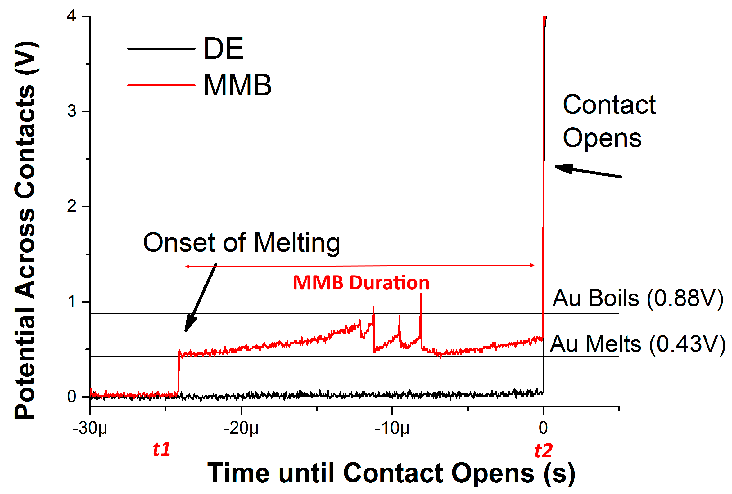
The main obstacle to a highly reliable Ohmic MEMS switch is the switching surface, which is associated with two factors leading to device failure. The first is where the contacts become stuck together through processes such as cold welding, thermal welding or the accumulation of adhesive wear polymers. The second is through damage and wear to the contact surface leading to an excessive increase in contact resistance [3,4]. Typically, the metallic films are 10′s or 100′s of nm in thickness with very limited tolerance to wear [2,5]. Mechanical effects of switching such as work hardening and cold-welding cause wear during switching with no electrical signal (cold switching). Operating the contacts while they carry an electrical signal (hot switching) of more than ~1 V and a several mA’s causes an additional mechanism for wear driven by Joule heating and is described by a process of fine transfer [6]. At contact opening, as the contact force decreases, the contact area shrinks, and the current flow lines are constricted. The current constriction causes Joule heating where even a small potential drop across the contact is sufficient to cause softening, melting and boiling of the contact material at the final point of contact [7,8,9,10]. As the contacts separate a molten metal bridge (MMB) is formed between the contacts, that ruptures as it boils, interrupting the circuit. The softening, melting and boiling voltages for Au are, respectively, ~0.08, 0.43 and 0.88 V [8,11]. The MMB wear is described by a fine transfer process linked to the gradual and cumulative scattering of the melted contact material [12]. If the contact area does not decrease smoothly and gradually, there may be a step change in the contact area. This represents a limiting case for the formation of an MMB [8,13]. Through in-situ surface measurement of thin film Au contacts between hot switching cycles, the contacts were observed to sometimes open without showing the characteristic MMB waveform. These events were linked to sections of the contact surface being torn away from the surface [14]. The event is therefore termed a Delamination Event (DE) [15]. The DE can be characterized with an immediate transition from the closed contact potential to the open contact potential.
Figure 1 shows waveforms which occur as the contacts open typical of the MMB (red graph) as the contact material melts, draws out a MMB that boils and ruptures before the contact opens, and the DE (black graph) as the contacts open instantaneously [10].
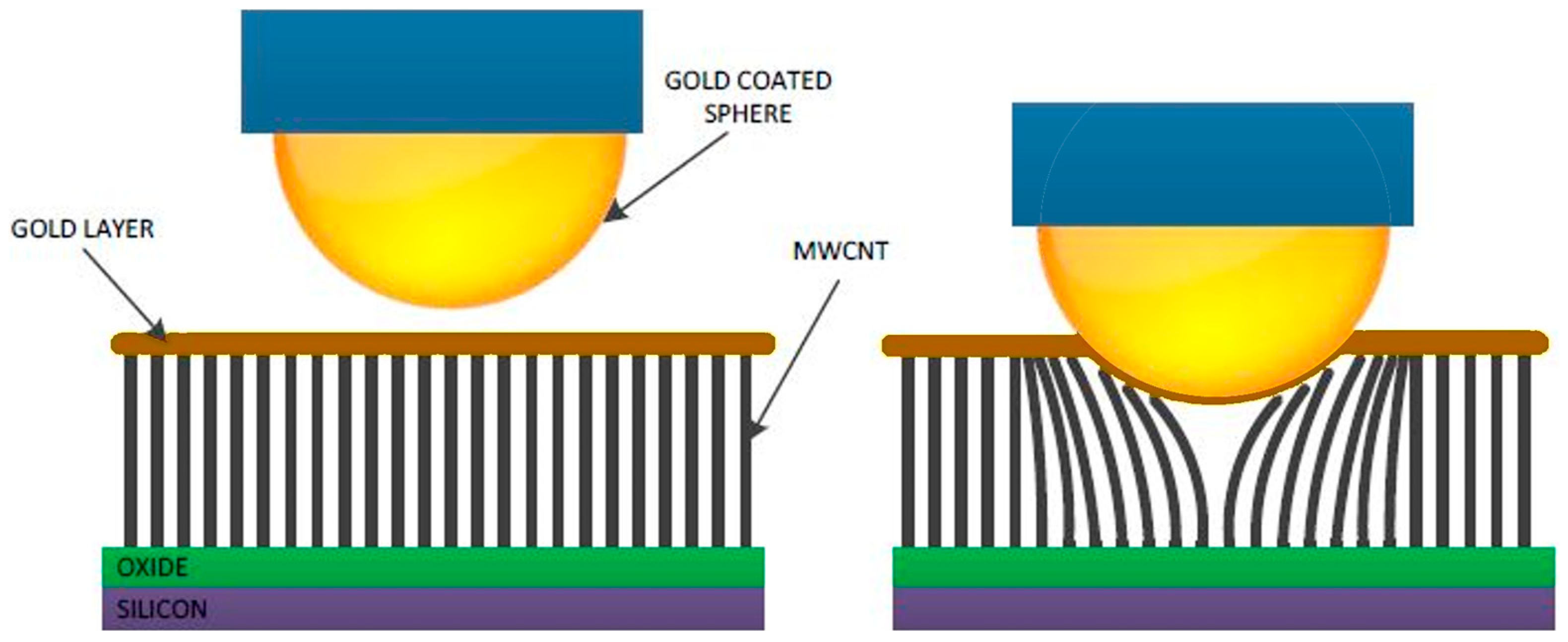
A proposed solution to the wear in thin Au films is a composite where the Au film is embedded in the upper surface of a forest of vertically aligned multi-walled carbon nanotubes (MWCNT) [16,17]. The carbon nanotubes provide a mechanically compliant sublayer, allowing the conductive Au to conform to the incoming contact (Figure 2). This provides reduced contact pressure, increased contact area, and a mechanism to absorb the kinetic energy of contact closure [18], when compared to thin film Au-Au contacts. The vertical alignment of the nanotubes is crucial in achieving the extended lifetime as random or non-vertical alignments provide negligible benefit [19]. Au/MWCNT has been shown to increase contact lifetime [20]. Switching lifetimes of 4 × 10⁹ cycles at 4 µW DC power and 150 × 106 cycles at 200 mW DC power have been demonstrated with the material [15,21].
In this study, transient forces associated with the contact opening processes are investigated. The contacts are actuated by a piezoelectric cantilever to simulate MEMS scale closure force (150 µN) under low current hot switching conditions (4 V DC 20 mA). Contact force and potential are then monitored as the contact opens.
2. Materials and Methods
2.1. Contact Manufacture
The test contacts are: (1) an hemispherical upper contact, manufactured from a 2 mm diameter precision ground stainless-steel ball, coated with 20 nm Cr, then 500 nm Au and (2) a planar lower contact, of a SiO2 on Si substrate (IDB Technologies, Andover, UK), with a 50 µm field of vertically-aligned multiwalled carbon nanotubes (MWCNT) grown by the thermal chemical vapour deposition (tCVD) of ethylene in a quartz reactor tube furnace. The MWCNT upper surface is coated with a 500 nm layer of Au by plasma-enhanced chemical vapour deposition (peCVD) (LAB Line, Kurt J Lesker, Jefferson Hills, PA, USA). Height and layer thickness are verified by exposing masked sections and measuring the step height with a laser surface profiler (Xyris 4000CL, TaiCaan Technologies, Southampton, UK).
2.2. Test Circuit
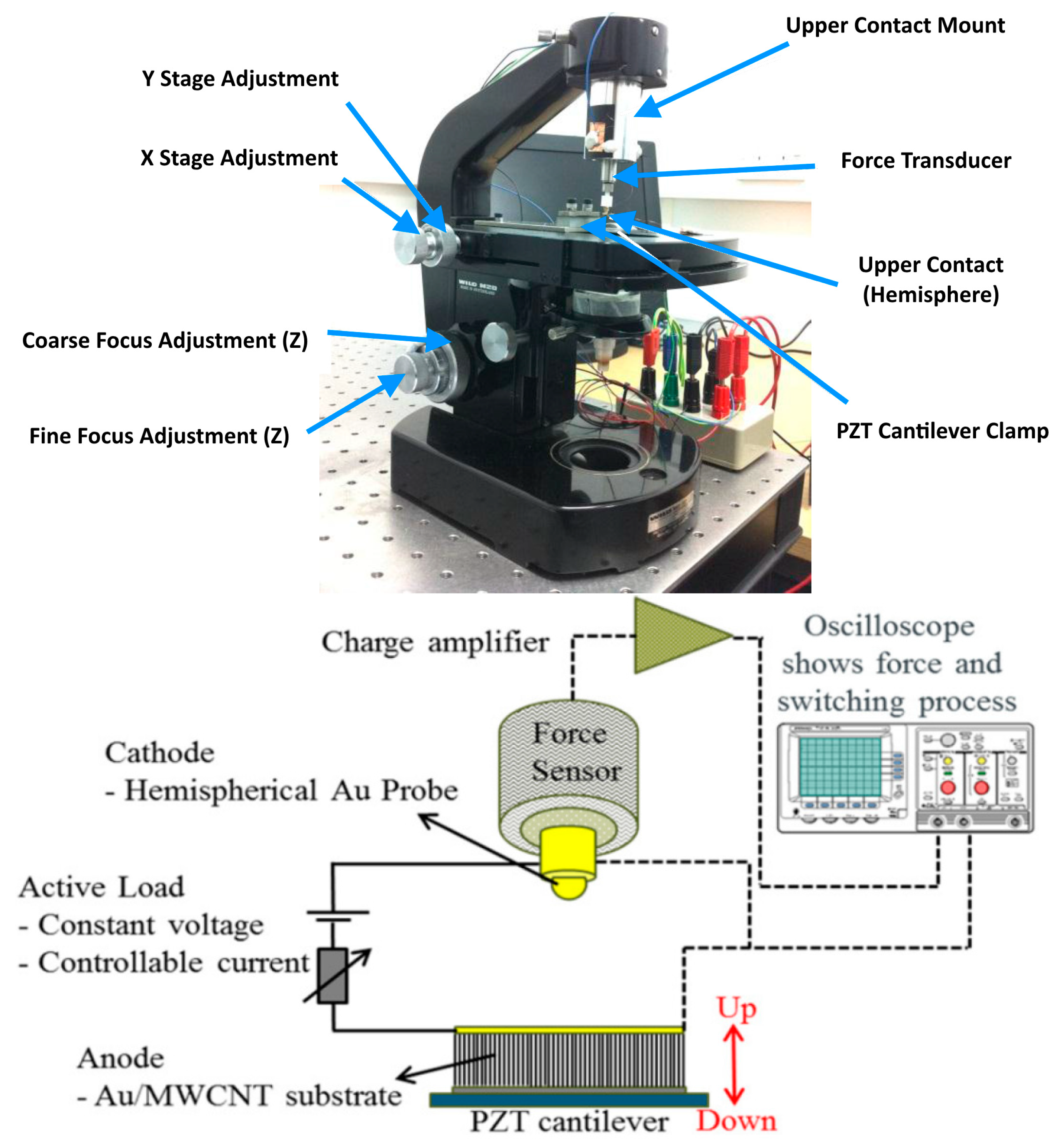
The switching circuit is a simple series loop incorporating a 4 V lead acid battery with current controlled by a resistive load. The contact potential is measured by a high-speed oscilloscope (MDO4054-3, Tektronix, Beaverton, OR, USA) with 1 GHz bandwidth and a sample rate of 2.5 GS/s (0.4 ns time resolution). The circuit conditions are 4 V DC and 20 mA, chosen as they provide conditions where a mixture of MMB and DE type contact openings are expected [15]. The circuit configuration for switching is shown in Figure 3.
2.3. Switching Arrangement and Force Measurement
The test apparatus uses a frame, stage and focus controls of an optical microscope to position the two contacts. The upper Au coated ball contact is fixed to the tip of a quartz force sensor (Model 9207, Kistler Group, Winterthur, Switzerland) with 115 pC/N sensitivity, that is fixed to the head of the microscope frame. The lower contact is fixed to a piezoelectric cantilever suspended from the stage of the microscope frame. The switch is actuated by a square wave voltage provided by a signal generator. The system is housed inside a chamber to stabilize temperature and damp air transmitted vibration. The apparatus is isolated from floor transmitted vibrations by an optical grade damping table (PG Series Breadboard with ND30A isolators, Newport, Irvine, CA, USA). The force transducer is linked to a charge amplifier (Kistler Type 5007, Kistler Group, Winterthur, Switzerland) with -3db frequency response at 2.3 GHz. The sensitivity for transient force is ~1 µN. The method is highly sensitive to changes in dynamic forces but is described as a quasi-static force measurement because the charge associated with a static force will decay over longer periods. The time constant for charge decay is set to 0.01 s. The apparatus is housed in a metrology laboratory with temperature and humidity controlled to better than 22.0 ± 0.2 °C and 40 ± 10%RH.
2.4. Experimental Procedure
The contacts are positioned to achieve a static closed contact force of 150 µN. The static closed force is determined using the same charge amplifier with a 20 s time constant. The contacts are opened to a clearance of ~25 µm by applying a 20 V signal to the piezoelectric cantilever. The contact closes when the signal to the piezoelectric cantilever is 0 V. The drive signal to the cantilever is an offset 0–20 V square wave 0.5 Hz signal. The contacts open ~250 µs after the drive signal to the cantilever reaches 20 V. The contacts are ‘bedded in’ for 1000 cycles with no circuit load to allow the contact interface to mechanically stabilize. After 1000 cycles with no electrical signal, the load circuit is switched on. A further 100 cycles are carried out hot switching a 4 V DC, 20 mA signal. The contact potential and transient forces associated with these 100 contact openings are captured. The voltage and force signals are sampled at 0.4 ns over 80 µs (200,000 points).
2.5. Capture and Classification of Contact Opening Events
The point of contact opening is defined as occurring when the measured voltage exceeds 3 V. The opening event type is determined from the duration of the opening event.
Because the contact softening voltage (~0.08 V) is close to the resolution of the oscilloscope (0.02 V), the onset of contact melting is defined by applying a moving average filter. The filter removes the rapid fluctuations and allows the onset of contact softening to be distinguished from background noise. The contact opening waveform is resampled by the filter over a 2 µS window at 51-points. The starting point of the opening event, t1, is defined as where the filtered waveform value rises to 0.08 V above closed contact potential for consecutive samples. The end point, t2, of the opening event is defined as where the contact potential rises above 3 V. The opening event duration is the time elapsed between t1 and t2 as shown in Figure 1. This method gives a sensitivity to detect the opening event duration of ~2 µs.
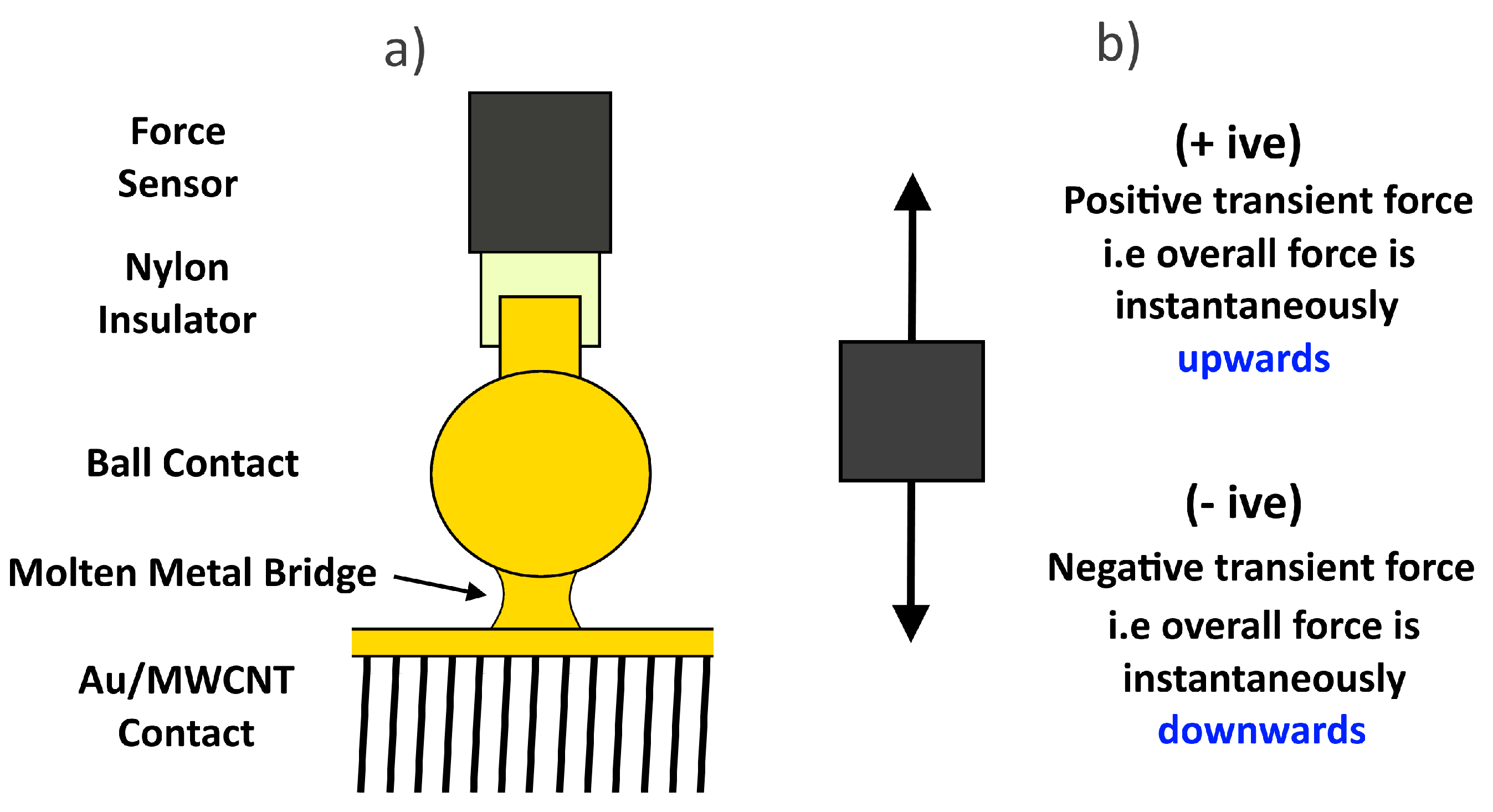
The peak magnitude of force after the contact opens (potential exceeds 3 V) is defined as the Transient Peak Force. The arrangement of the contacts and a free body diagram showing the force sensor and the convention used for force direction is shown in Figure 4. Examples of Transient Peak Force are shown in Figure 5.
3. Results
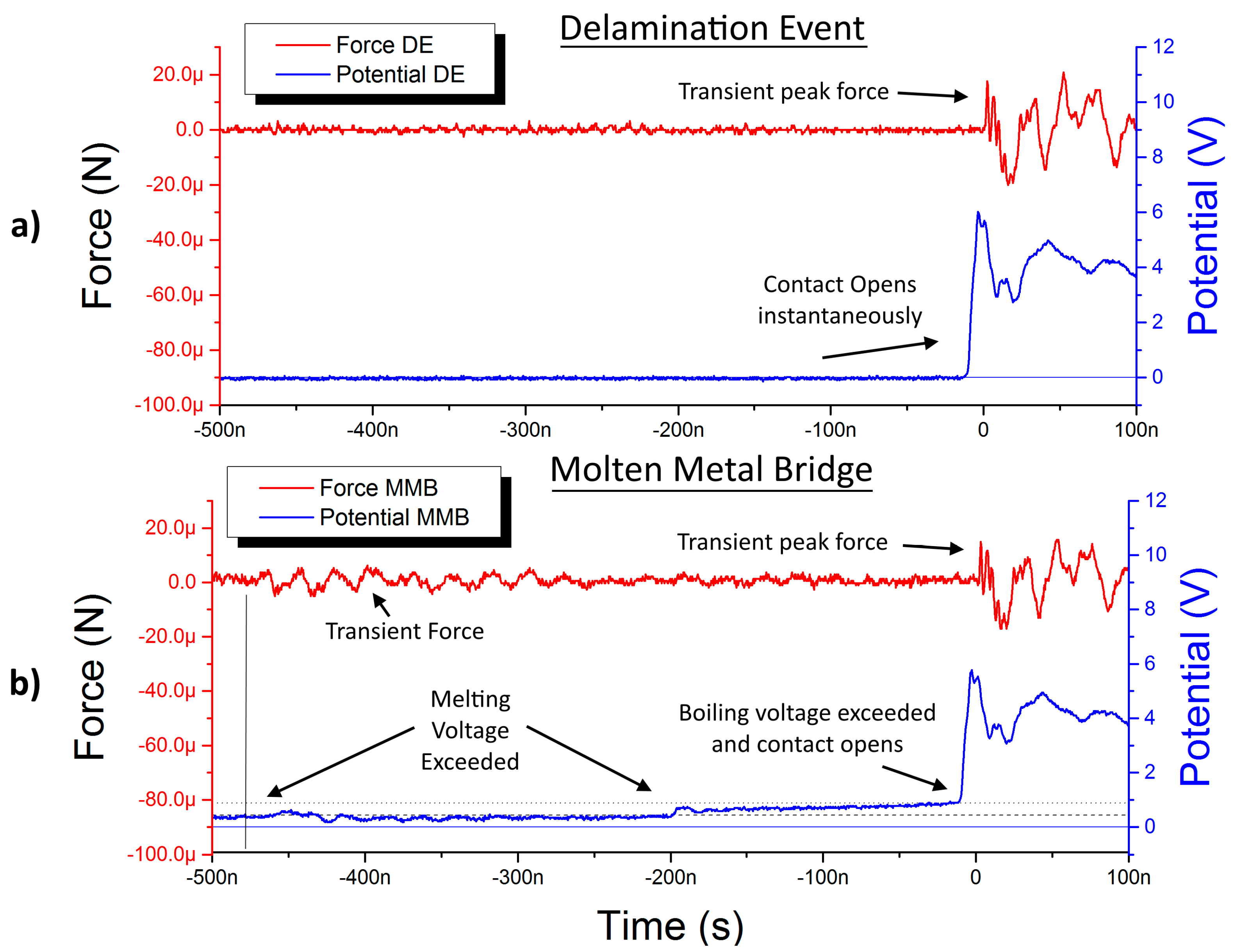
Figure 5 shows the voltage and force transients at opening. The figure compares a DE (top) and MMB (bottom) from 500 ns before to 100 ns after the contact opens.
The DE force graph in Figure 5a (red trace) shows the force sensor at the noise floor (~1 µN) while the contact potential graph in Figure 5a (blue trace) remains at the closed contact potential. At time = 0 the contact potential instantly rises above the open circuit voltage and a positive force event around 20 µN is detected. Both force and the voltage potential oscillate after this event.
The MMB force graph in Figure 5b (red trace) shows force events above the noise floor of the force sensor. The contact potential varies above the normal closed contact potential, with steps shown to correspond with the melting voltage (horizontal dashed line) and boiling voltage (dotted black line) for Au. The contact potential rises to the boiling voltage for Au where it then rapidly rises above the open circuit voltage and a positive force event of ~20 µN is detected. The force and voltage oscillations observed are similar in both MMB and DE examples.
3.1. The Molten Metal Bridge and the Transient Contact Force
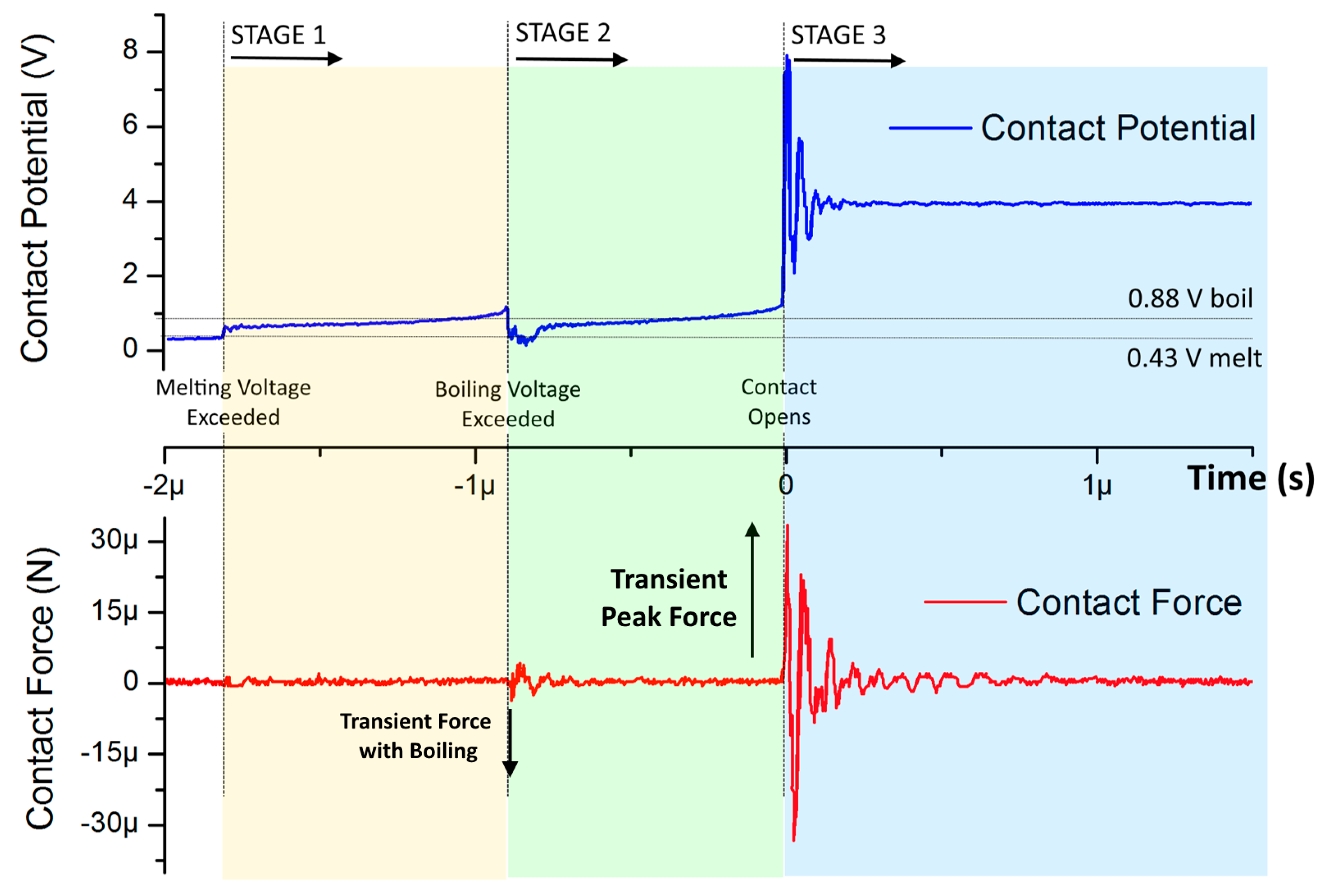
While each MMB event is unique, a representative example is presented in Figure 6, over a longer time duration that Figure 5. Contact potential (blue) and the transient force (red) are shown from 2 µS before to 1.5 µS after contact opening. The time scale shows t = 0 s as the contact opening.
3.1.1. Stage 1—Melting Voltage Exceeded (from ~1.8 µs before Contact Opening)
As the contact potential steps from just below 0.4 V to above 0.6 V (this is above the melting voltage for Au), there is a very low-level force that is within the noise level of the sensor. At the end of stage 1, the contact potential rises to 0.9 V before rapidly increasing to 1.1 V, exceeding the boiling voltage for Au at time = −0.9 µS. The rapid increase from 0.9 V to 1.1 V occurs over 30 nS.
3.1.2. Stage 2—Boiling Voltage Exceeded (from ~0.9 µs before Contact Opening)
At the start of stage 2, the contact potential drops sharply from 1.1 V to 0.2 V. After a further 150 ns, the contact potential rises back to 0.6 V. When the contact potential drops from 1.1 V to 0.2 V, a force transient is detected, peaking at 5 µN and lasting 150 ns. The force is initially in the opposite direction to the transient peak force in Figure 6 and is damped after 150 ns. From t = −0.75 µs, the contact potential slowly rises from 0.6 V to 0.9 V and above the boiling voltage. The contact potential increases more rapidly from 0.9 V to 1.1 V over 100 ns before a step change to nearly 7.8 V occurs.
3.1.3. Stage 3—Contact Opens
This is the point at which the contacts are deemed to be open and the circuit has been interrupted. After the circuit is open, the contact potential oscillates 5 times over 260 ns around the open circuit voltage of 4.1 V varying between a maximum of 7.8 V and a minimum of 2.2 V. The time period of each oscillation in contact potential is 52 ns. The force is initially positive and then oscillates 8 times over the next 700 ns with a time period of 87 ns. The peak force when the contact opens is the Transient Peak Force.
3.2. The Classification of Delamination Events (DE) and Molten Metal Bridge (MMB) Events
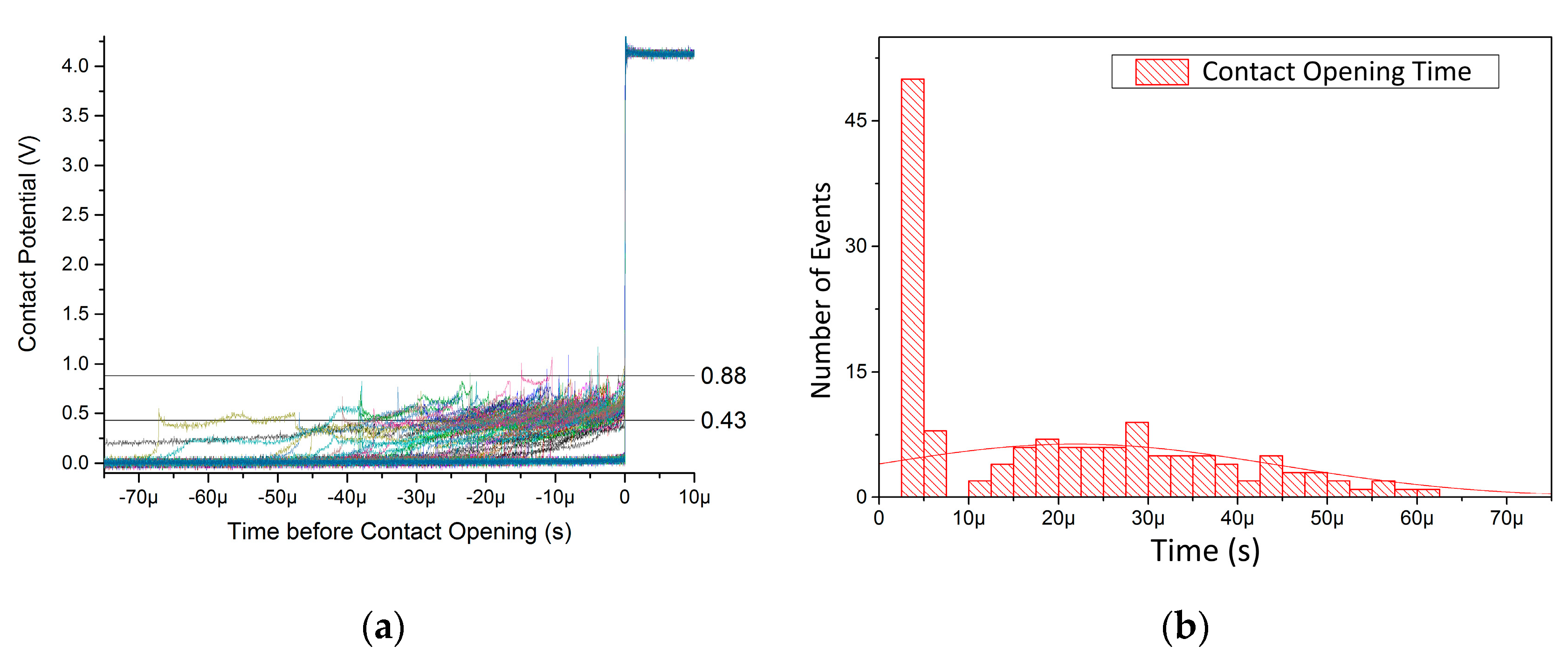
The type of opening event is classified by the transient voltage waveform. DE shows a single abrupt voltage step to the open circuit voltage, whereas MMB shows multiple stages of rising and falling contact potential as the bridge is formed. Figure 7 shows 100 consecutive opening events as both contact potential vs time (Figure 7a) and the number of events of a given duration (Figure 7b). The MMB event waveforms are highly variable from one event to the next. It has previously been shown that groups of consecutive cycles at the same switching conditions are well described by a Gaussian distribution [10]. It is possible to distinguish a clear difference between the DE and MMB events in Figure 7a as there are no MMBs apparent with a duration of less than ~10 µs. However, it is difficult to see the number of DE as each trace is effectively overlaid. By evaluating the duration of each event and plotting the number of events at a given duration (Figure 7b) it is very clear that there are two distinct types of events. Approximately half the events are classified with a duration under 7.5 µs while the remainder have a duration above 10 µs. Using this methodology, the short duration events are classified as DE and the longer duration events as MMB. No events are classified with a duration between 7.5 and 10 µs.
With the contact opening now classified as either MMB or DE, the contact force can be evaluated and according to the type of opening event.
3.3. The Contact Opening Force for Delamination and Molten Metal Bridge Events
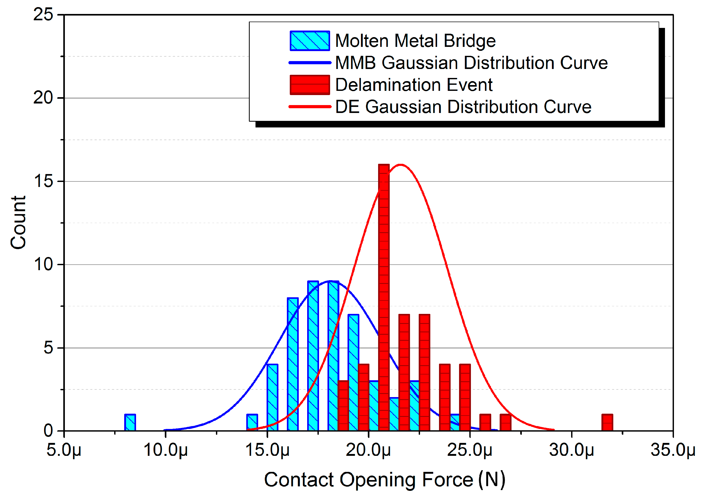
Figure 8 shows a histogram distribution of the Transient Peak Force of the 100 hot switched (4 V DC, 20 mA) opening events. The colour scale shows the contact opening type by colour with MMB (blue) and DE (red) with a normal distribution curve fitted to each type. The figure demonstrates a nearly equal number of DE and MMB events.
The distribution of Transient Peak Force for MMB is close to a Gaussian distribution with a mean opening force and standard deviation of 18.1 ± 2.5 µN. The distribution of the DE type demonstrates a slightly more leptokurtic (peakier) distribution with a higher mean opening force of 21.6 ± 2.3 µN. This represents the DE contact openings having a ~20% higher average Transient Peak Force than the MMB type.
4. Discussion
4.1. The Molten Metal Bridge and the Transient Contact Force
The results show that the MMB event can be detected by the force sensing method. The force events are synchronized with step changes in the contact potential linked to phase changes in the contact material predicted by the ϑ-ψ theorem [9].
4.1.1. Stage 1—Melting Voltage
The first force event is a small shock or vibration caused by liquid surface tension as the MMB is formed. The observed force indicates that as the liquid bridge initially forms, there is a small increase in adhesion force. Over the following 900 ns, the contact potential rises smoothly as the constriction resistance increases, with no force transients detected at the contact. This indicates the contacts are separating while the molten bridge is elongating and decreasing in cross section while its temperature rises.
4.1.2. Stage 2—Boiling Voltage
As the contact potential reaches 0.9 V, it begins to rise more quickly, reaching 1.1 V before suddenly dropping to 0.2 V in Figure 6. The observed drop in potential across the contact shows the current path has rapidly decreased in resistance. This suggests that on this occasion the circuit path is not interrupted by the onset of boiling but rather it has been deformed or distorted to include a part of the contact that is much cooler and is still in solid phase. This event is not typical and is attributed to the unique properties of the Au/MWCNT surface. The MWCNT under the Au coating acts like a spring with the deformation of the surface returning its non-loaded condition. The introduction of cooler material to the MMB momentarily reduces the average temperature of the bridge to below the melting (freezing) point for around 80 ns before the potential again exceeds the melting voltage. This period is explained by the new solid material becoming heated to a molten state.
As the contacts separate, the refreezing of MMB causes an instantaneous force. This is experienced as a force by the force transducer, followed by a mechanical ringing that is damped as the bridge re-liquifies. It is noted that this is in the opposite direction to the defined Transient Peak Force and indicates that the Au/MWCNT surface is applying a force to the upper contact, as would be expected with the spring-like nature of the surface.
4.1.3. Stage 3—Contact Opening
Prior to Stage 3 in Figure 6 the potential rises steadily from 0.6 to 0.9 V, before again increasing more rapidly after reaching 0.9 V; however, this time, the contact potential rises instantaneously (in less than 4 ns) to over 3 V. Simultaneously, a sudden increase in force of 32 µN is detected at the upper contact. This event describes the rupture of the molten bridge by boiling, and the contacts separate. For the contacts to separate they must be under enough opening force to overcome the adhesive forces between the contacts. As the MMB boils it is broken and the surface tension that was acting as an adhesive force between contacts is instantaneously removed. The measured Transient Peak Force is the upper contact experiencing a sudden decrease in adhesive force as the MMB is removed. The measured Transient Peak Force is therefore equal and opposite to the adhesive tension force in the MMB the instant before the bridge ruptures.
After the contacts have separated there is a transient ringing in both the electrical circuit and the response of the force transducer. The oscillation in force can be explained as mechanical vibration of the upper contact as MMB ruptures and its tension force is lost. The vibration characteristics are therefore related to the stiffness and the mass of the upper contact mount [24]. It is interesting to note that the time period of force and contact potential oscillations are of the same order at 52 and 87 ns, respectively. Similar phenomena were reported during opening of MEMS scale contacts; however, the study used extremely low opening velocities that were unrepresentative of a practical device and subject to influence from environmental vibration [25].
4.1.4. Modelling Voltage Oscillation after Contact Separation
The observation of oscillation in contact potential following contact separation appears highly repeatable, suggesting a ringing response in the electrical circuit. The response is modelled to check the empirically observed response matches the predicted response. The over voltage at the point of circuit rupture must be maintained below ~12 V as above this level micro arcing can be induced. The magnitude and time period consistent with the circuit’s inductance and capacitance are estimated from a series LCR model of the switching circuit behavior (Matlab Simulink 2015) according to the second order transient response (1).
Capacitance is estimated using a parallel plate model, while inductance is estimated as the self-inductance of a single loop of wire. The modelled and empirically observed values for overvoltage, time period and damping time of the electrical ringing response are summarized in Table 1.
The modelled values for peak overvoltage and the frequency of the response closely correlate with the experimentally observed voltage transient at contact opening. The damping observed is higher than that predicted by the model. This is expected as the model does not consider the influence of circuit capacitance changing (as would occur between real separating contacts) or the dynamic impedance of the lead acid voltage source to a high frequency signal, both factors that would damp the response. The good agreement observed between the modelled and empirically observed values for overvoltage and frequency support the observation that the oscillation in the contact potential is the circuit electrically ringing after opening due to its micro-inductance and pico-capacitance. Both empirical and modelled responses indicate the MMB test circuit does not exceed the threshold voltage for arcing [11].
A continuous increase in separation of contacts means the capacitance will change dynamically. More advanced modelling of capacitance and load circuit inductance is identified for future investigation.
4.2. Classification of MMB and DE
The classification of opening events by duration demonstrates a distribution with a clear region of separation. This shows the classification method is effective at separating the MMB and DE events. It is noted that the use of the moving average filter will result in overestimated DE duration, which is effectively instantaneous, but the primary purpose is to classify the opening event type and this method provides a clear distinction between MMB and DE. The switching conditions were chosen as they have previously been linked to a frequent occurrence of the DE. The occurrence of DE marks a limiting condition for the formation of the MMB. Increasing the current of voltage from circuit conditions of 4 V 20 mA demonstrated that the number of DE decreased, while as the number of switching cycles increased the frequency of the DE increased [15]. The limiting case to the formation for the MMB can be explained by step changes in the conduction area. A requirement for the Holm ϑ-ψ theorem is that Joule heating raises the conductor temperature nearly instantaneously to a point of thermal equilibrium [8]. This is a reasonable assumption provided the contact area and therefore constriction resistance change gradually. If there is a step change in the contact area occurring (such as a delamination), this may occur too rapidly for thermal equilibrium so no MMB is formed. The time constant for thermal equilibrium is dependent only on the thermal conductivity and heat capacity per unit volume of the conducting material and is proportional to the contact area. Illustratively, for a circular constriction of diameter 10 µm in a Au conductor, the thermal equilibrium time constant is calculated as 0.198 µs. It is noted that the observed MMB duration and contact areas reported in low force studies of the Au/MWCNT material are of similar magnitude [10,14].
4.3. Distribution of Contact Opening Force
The distribution of Transient Peak Force shows that DE is associated with a greater adhesion force between contacts than the MMB events. Figure 9 shows scanning electron micrographs of the Au/MWCNT contact surface before and after hot switching at 4 V DC and 20 mA. There is evidence of both softening and melting as well as mechanical flattening and cracking of the surface. The appearance of spherical particles of Au several µm in diameter is observed after hot switching. The mechanism of formation is proposed to be the MMB with the particle size linked to the magnitude of the MMB. It is interesting to note that the spherical particles are embedded into the surface and the largest appear separated from the remaining Au surface. A secondary feature detected after hot switching are flattened regions with irregular edges. One such feature is shown at higher magnification, with cracks in the surface ~1.5 µm apart (blue arrows) apparent and suggests the surface has weakened.
It is proposed that because of the speed of the DE there is insufficient time for an MMB to form. The Transient Peak Force observed is evidence the adhesive forces released during a DE are ~20% greater than during the MMB formed under 4 V 20 mA circuit conditions.
In the MEMS switching regime, contact opening force is limited. Small increases in adhesion are therefore linked to increase risk of the contact failure by sticking [24]. It has previously been shown that varying the circuit conditions will influence the duration, thermal energy and size of the MMB [10].
5. Conclusions
The contact opening force in molten metal bridge (MMB) and delamination event (DE) have been investigated during hot switching of a Au/MWCNT composite contact at forces and switching conditions representative of the MEMS switch regime.
The magnitude and direction of micro force transients are observed under contact closure force and opening velocities realistic for a practical device. The force transients are linked to the melting and boiling processes that are also linked to a fine transfer wear process. A limiting case for the formation of the MMB is proposed where step changes in contact area occur too rapidly for thermal equilibrium.
Finally, the transient contact force as the contacts open—defined as the Transient Peak Force—is found to be ~20 % greater when DE are observed cf. MMB events.
Author Contributions
Conceptualization, J.W.M. and T.G.B.; methodology, T.G.B.; investigation, T.G.B.; resources, J.W.M.; writing—original draft preparation, T.G.B.; writing—review and editing, T.G.B. and J.W.M.; supervision, J.W.M.; project administration, J.W.M.; funding acquisition, J.W.M.
Funding
This research was funded by the EPSRC grant EP/M508147/1.
Conflicts of Interest
The authors declare no conflict of interest.
References
- Iannacci, J. RF-MEMS: An enabling technology for modern wireless systems bearing a market potential still not fully displayed. Microsyst. Technol. 2015, 21, 2039–2052. [Google Scholar] [CrossRef]
- Coutu, R.A., Jr.; Kladitis, P.E.; Leedy, K.D.; Crane, R.L. Selecting metal alloy electric contact materials for MEMS switches. J. Micromech. Microeng. 2004, 14, 1157. [Google Scholar] [CrossRef]
- Toler, B.F.; Coutu, R.A.; McBride, J.W. A review of micro-contact physics for microelectromechanical systems (MEMS) metal contact switches. J. Micromech. Microeng. 2013, 23, 10. [Google Scholar] [CrossRef]
- Basu, A.; Adams, G.; McGruer, N. A review of micro-contact physics, materials, and failure mechanisms in direct-contact RF MEMS switches. J. Micromech. Microeng. 2016, 26, 104004. [Google Scholar] [CrossRef]
- Spearing, S.M. Materials issues in microelectromechanical systems (MEMS). Acta Mater. 2000, 48, 179–196. [Google Scholar] [CrossRef]
- McBride, J. The wear processes of gold coated multi-walled carbon nanotube surfaces used as electrical contacts for micro-electro-mechanical switching. Nanosci. Nanotechnol. Lett. 2010, 2, 357–361. [Google Scholar] [CrossRef]
- Price, M.; Jones, F.L. The electrical contact: The properties and rupture of the microscopic molten metal bridge. J. Phys. D Appl. Phys. 1969, 2, 589. [Google Scholar] [CrossRef]
- Slade, P.G. Electrical Contacts: Principles and Applications, 2nd ed.; CRC Press: Boca Raton, FL, USA, 2014. [Google Scholar]
- Holm, R. Electric Contacts: Theory and Application; Springer Science & Business Media: Berlin, Germany, 1958. [Google Scholar]
- Bull, T.; Mcbride, J. The Influence of Circuit Parameters on Molten Metal Bridge Energy in a MEMS relay testing platform. In Proceedings of the 2016 Twenty Eighth International Conference on Electrical Contacts, Edinburgh, UK, 6–9 June 2016. [Google Scholar]
- Doduco. Databook of Electrical Contacts; Duduco GmbH: Pforzheim, Germany, 2012. [Google Scholar]
- McBride, J.W.; Liu, H.; Chianrabutra, C.; Lewis, A.P. The Wear of Hot Switching Au/Cr-Au/MWCNT Contact Pairs for MEMS Contacts. IEICE Trans. Electron. 2015, E98c, 912–918. [Google Scholar] [CrossRef]
- Timsit, R.S. Constriction resistance of thin film contacts. IEEE Trans. Compon. Packag. Technol. 2010, 33, 636–642. [Google Scholar] [CrossRef]
- Bull, T.G.; McBride, J.W. In-Situ Contact Surface Characterization in a MEMS Ohmic Switch under Low Current Switching. Technologies 2018, 2, 47. [Google Scholar] [CrossRef]
- Bull, T.G.; McBride, J.W.; Jiang, L. The influence of Circuit Parameters on Molten Bridge Surface Degradation in a Au/MWCNT MEMS Switch Contact. In Proceedings of the 2018 IEEE Holm Conference on Electrical Contacts, Albuquerque, NM, USA, 14–18 October 2018; pp. 359–365. [Google Scholar]
- Mcbride, J.; Yunas, E.; Spearing, S. Gold coated Carbon Nanotube Surfaces as Low Force Electrical Contacts for MEMS devices: Part 1. In Proceedings of the 59th IEEE Holm Conference on Electrical Contacts, Newport, RI, USA, 22–25 September 2013. [Google Scholar]
- McBride, J.; Yunus, E.; Spearing, S. Improving the contact resistance at low force using gold coated carbon nanotube surfaces. Eur. Phys. J. Appl. Phys. 2010, 50, 12904. [Google Scholar] [CrossRef]
- Down, M.; Lewis, A.P.; Jiang, L.; McBride, J.W. A nano-indentation study of the contact resistance and resistivity of a bi-layered Au/multi-walled carbon nanotube composite. Appl. Phys. Lett. 2015, 106, 101911. [Google Scholar] [CrossRef] [Green Version]
- Kageyama, T.; Shinozaki, K.; Zhang, L.; Lu, J.; Takaki, H.; Lee, S.-S. Fabrication of an Au–Au/carbon nanotube-composite contacts RF-MEMS switch. Micro Nano Syst. Lett. 2018, 6, 6. [Google Scholar] [CrossRef]
- Lewis, A.P.; McBride, J.W.; Jiang, L. Evolution of Voltage Transients During the Switching of a MEMS Relay with Au/MWCNT Contacts. IEEE Trans. Compon. Packag. Manuf. Technol. 2015, 5, 1747–1754. [Google Scholar] [CrossRef]
- McBride, J.W.; Bull, T.G. The in-situ wear of a hot and cold switched Au on Au coated MWCNT electrical contact for a MEMS switch application. In Proceedings of the IEEE Holm Conference on Electrical Contacts, Milwaukee, WI, USA, 14–18 September 2019. [Google Scholar]
- Lewis, A.; Chianrabutra, C.; Down, M.; McBride, J.; Jiang, L.; Spearing, S. Carbon nanotube composite surfaces for electrical contact interfaces. In Proceedings of the IeMRC 7th Annual Conference, Loughborough, UK, 5 September 2012. [Google Scholar]
- McBRIDE, J.W.; Chianrabutra, C.; Jiang, L.; Pu, S.-H. The contact resistance performance of gold coated carbon-nanotube surfaces under low current switching. IEICE Trans. Electron. 2013, 96, 1097–1103. [Google Scholar] [CrossRef]
- Jensen, B.D.; Huang, K.W.; Chow, L.L.W.; Kurabayashi, K. Adhesion effects on contact opening dynamics in micromachined switches. J. Appl. Phys. 2005, 97. [Google Scholar] [CrossRef]
- Ren, W.; Chang, C.; Chen, Y.; Xue, S.; Coutu, R.A. Investigation of the Surface Adhesion Phenomena and Mechanism of Gold-Plated Contacts at Superlow Making/Breaking Speed. IEEE Trans. Compon. Packag. Manuf. Technol. 2015, 5, 771–778. [Google Scholar]
Figure 1.
The contact potential during two hot switched opening events of a Au/MWCNT contact switched at 4 V and 20 mA. The red trace is characteristic of a molten metal bridge forming with steps linked to the melting and boiling voltages for Au. The black trace is characteristic of a delamination event (DE) that shows no evidence of the contact material melting or boiling.

Figure 2.
Illustration showing a composite contact formed by Au coating a field of vertically aligned multi-walled carbon nanotubes. The composite conforms to the incoming contact, enhancing the contact area and reducing the contact pressure [22].
Figure 2.
Illustration showing a composite contact formed by Au coating a field of vertically aligned multi-walled carbon nanotubes. The composite conforms to the incoming contact, enhancing the contact area and reducing the contact pressure [22].

Figure 3.
Switching circuit arrangement and experimental apparatus [23].
Figure 3.
Switching circuit arrangement and experimental apparatus [23].

Figure 4.
The contact force measurement arrangement (a) and a free body diagram of the force sensor showing the convention used in graphs for positive and negative force (b).
Figure 4.
The contact force measurement arrangement (a) and a free body diagram of the force sensor showing the convention used in graphs for positive and negative force (b).

Figure 5.
Examples of the force and contact voltage during a Delamination Event (a) and Molten Metal Bridge (b) from 500 ns before the contact opens with the Transient Peak Force as the contact opens indicated.
Figure 5.
Examples of the force and contact voltage during a Delamination Event (a) and Molten Metal Bridge (b) from 500 ns before the contact opens with the Transient Peak Force as the contact opens indicated.

Figure 6.
Molten metal bridge contact potential and the corresponding Transient Peak Force.

Figure 7.
The transient voltage waveforms of 100 consecutive switching cycles (a) and a histogram showing the calculated duration of the opening event (b). The individual molten metal bridge (MMB) waveforms are highly variable but rise to 0.43 and 0.88 V prior to opening. The delamination event (DE) show no increase in the contact potential until the contact abruptly opens.

Figure 8.
A histogram of the Transient Peak Force of 100 consecutive hot switched contact openings at 4 V 20 mA. Delamination event (DE) are shown in red while molten metal bridge (MMB) are shown in blue. The average Transient Peak Force is 18.1 µN for MMB and 21.6 µN for DE.
Figure 8.
A histogram of the Transient Peak Force of 100 consecutive hot switched contact openings at 4 V 20 mA. Delamination event (DE) are shown in red while molten metal bridge (MMB) are shown in blue. The average Transient Peak Force is 18.1 µN for MMB and 21.6 µN for DE.

Figure 9.
Electron micrographs of the Au/MWCNT surface before switching (top left) and after hot switching 1,000,000 cycles at 4 V 20 mA (top right). The main image (bottom) is magnified to show cracks in the surface (blue arrows) next to a region where Au is being worn away.
Figure 9.
Electron micrographs of the Au/MWCNT surface before switching (top left) and after hot switching 1,000,000 cycles at 4 V 20 mA (top right). The main image (bottom) is magnified to show cracks in the surface (blue arrows) next to a region where Au is being worn away.


Table 1.
Modelled vs Observed Electrical Ringing Characteristics at Contact Opening.
| Peak Over Voltage (V) | Time Period (ns) | Damping Time /6dB (ns) | |
|---|---|---|---|
| Experimental | 3.7 | 52.5 | 260 |
| Modelled | 3.8 | 69.4 | 427 |
© 2019 by the authors. Licensee MDPI, Basel, Switzerland. This article is an open access article distributed under the terms and conditions of the Creative Commons Attribution (CC BY) license (http://creativecommons.org/licenses/by/4.0/).
Share and Cite
MDPI and ACS Style
Bull, T.G.; McBride, J.W. Transient Contact Opening Forces in a MEMS Switch Using Au/MWCNT Composite. Technologies 2019, 7, 69. https://0-doi-org.brum.beds.ac.uk/10.3390/technologies7040069
AMA Style
Bull TG, McBride JW. Transient Contact Opening Forces in a MEMS Switch Using Au/MWCNT Composite. Technologies. 2019; 7(4):69. https://0-doi-org.brum.beds.ac.uk/10.3390/technologies7040069
Chicago/Turabian StyleBull, Thomas G., and John W. McBride. 2019. "Transient Contact Opening Forces in a MEMS Switch Using Au/MWCNT Composite" Technologies 7, no. 4: 69. https://0-doi-org.brum.beds.ac.uk/10.3390/technologies7040069
Note that from the first issue of 2016, this journal uses article numbers instead of page numbers. See further details here.