Article

SET Pulse Characterization and SER Estimation in Combinational Logic with Placement and Multiple Transient Faults Considerations †

by
Georgios Ioannis Paliaroutis
1,*,
Pelopidas Tsoumanis
1,*,
Nestor Evmorfopoulos
1,
George Dimitriou
1,2 and
Georgios I. Stamoulis
1,2
1
Department of Electrical and Computer Engineering, University of Thessaly, 38221 Volos, Greece
2
Department of Computer Science, University of Thessaly, 35131 Lamia, Greece
*
Authors to whom correspondence should be addressed.
This paper is an extended version of our paper published in the Proceedings of the 8th International Conference on Modern Circuits and Systems Technologies on Electronics and Communications (MOCAST 2019), Thessaloniki, Greece, 13–15 May 2019.
Submission received: 2 December 2019 / Revised: 31 December 2019 / Accepted: 7 January 2020 / Published: 10 January 2020
(This article belongs to the Special Issue MOCAST 2019: Modern Circuits and Systems Technologies on Electronics)

Abstract

:
Integrated circuit susceptibility to radiation-induced faults remains a major reliability concern. The continuous downscaling of device feature size and the reduction in supply voltage in CMOS technology tend to worsen the problem. Thus, the evaluation of Soft Error Rate (SER) in the presence of multiple transient faults is necessary, since it remains an open research field. In this work, a Monte-Carlo simulation-based methodology is presented taking into consideration the masking mechanisms and placement information. The proposed SER estimation tool exploits the results of a Single Event Transient (SET) pulse characterization process with HSPICE to obtain an accurate assessment of circuit vulnerability to radiation. A new metric, called Glitch Latching Probability, which represents the impact of the masking effects on a SET, is introduced to identify gate sensitivity and, finally, experimental results on a set of ISCAS’ 89 benchmarks are presented.

1. Introduction

Reliability has always been one of the major concerns for the VLSI industry, especially in recent years, as there were various challenges with the continuous shrinking of the integration technology [1]. Radiation-induced hazards occupy a central place in the range of reliability issues of Integrated Circuits (ICs). The most prevalent causes of such hazards are the alpha particles emitted from radioactive impurities in the package material of the ICs [2], and high-energy particles, mostly neutrons, from terrestrial cosmic rays [3] that may strike the silicon material of a chip. When such an incident occurs on a transistor, several electron-hole pairs are created which in turn, may be collected by the depletion region. This disturbance may momentarily cause a change of gate output logic state, which is well-known as a Single Event Transient (SET). The nature of this kind of errors is non-destructive but can affect the proper circuit operation and lead to system malfunction. However, such errors may have serious consequences in critical systems. These errors are called soft errors and Soft Error Rate (SER) indicates the grade of a circuit susceptibility to radiation-induced faults.
A drawback that follows the downscaling of the device feature size of ICs is that it renders them more vulnerable to radiation threats [4,5,6]. Thus, the need for identifying the impact of such errors on the circuit operation has become imperative and the contribution of simulation tools to the development of error-resistance chips tends to be significant.
In this work, we present a detailed overview of SER analysis for combinational logic, which focuses on the modeling and handling of multiple transients originated from a single particle strike. Based on Monte-Carlo simulations and considering ICs layout information [7], an accurate SER estimation is obtained. In addition, a series of spice experiments, with HSPICE [8], are conducted to characterize SET pulses for different design parameters, i.e., supply voltage, fan-outs, etc. Also, a new metric for the quantification of gate sensitivity is introduced, which is based on the impact that the three masking effects have on SET propagation up to the sequential components. Estimation of sensitivity is helpful for evaluating the variations of the circuit elements, as was done for example in the design of filters [9]. Extensive simulation results are presented for a variety of ISCAS’ 89 benchmark circuits. Some preliminary results of this paper were presented in [10].
The rest of the paper is organized as follows. Section 2 summarizes the related work on SER analysis; Section 3 introduces the basics of the SETs as well as the characterization of their pulse width; Section 4 presents the proposed methodology for SER estimation, whereas Section 5 describes the new metric for gate sensitivity identification; Section 6 presents the experimental results on the used benchmarks and, finally, Section 7 concludes this work.

2. Related Work

Over recent decades, extensive research was done on SER analysis, estimation, and mitigation of the ICs in order to deal with the challenges of the technology node downscaling. In this section, we present a variety of work related to the wide field of radiation-induced soft errors. A significant part of the bibliography involves SET pulse measurements through neutron beam testing setups that generate particles from a wide energy spectrum. The actual measurements in [11,12,13] provide useful results regarding the direct impact of radiation on ICs of various technology nodes and under different conditions. Although the real-time experiments comprise an important step to comprehend the behavior of modern chips into an environment of radiation fluxes, simulations are necessary to succeed scalability and obtain accurate results in a reasonable time. In [14,15,16], the authors characterize the SET pulse generation and propagation under different design parameters through SPICE and TCAD simulations.
With regard to SER estimation, extensive research has been conducted so far. Some of the methods are reviewed here as well as the state-of-the-art approaches. Most of the work implements the three natural masking mechanisms that mitigate SER, i.e., logical, electrical, and timing masking [17,18,19]. The works in [20,21] are based on probabilistic models and statistical methods for SER estimation. However, modern chips tend to be more vulnerable to high-energy particle strikes due to the technology downscaling and, thus, the reduction in the distance among the cells has increased the occurence of multiple transient faults (MTFs) caused by a single particle strike [22,23,24,25,26]. Therefore, recently, research in the particular field focuses on the SER evaluation in the presence of single event multiple transients (SEMTs). In [23], heavy-ion experiments are conducted to characterize the SEMTs. In [26,27], the authors introduce the identification of the cell sensitive regions for SER estimation. Some approaches consider that SEMTs occur at the output of physically adjacent gates, which are identified by examining the netlist [28,29]. Nevertheless, if only logic-level netlists are used for the determination of circuits’ error sites, neglecting the layout-level adjacency of the cells, may result in inaccurate estimation. Finally, other approaches provide a more realistic and reliable SER estimation analysis, by taking into consideration the circuit layout [26,27,30,31,32,33].

3. SET Modeling and Characterization

In this section, we present the model used for the generation of a transient fault (TF) through current pulse injection. We apply this model on spice simulations, thus, identifying the sensitive regions of a cell. Furthermore, spice simulations are performed for a range of different fan-outs, supply voltages and temperatures for each gate in order to characterize the transient pulse, so as to be integrated into the SER estimation tool. Finally, the SER verification framework is presented.

3.1. Current Pulse Model

When a high-energy neutron hits a sensitive region of a gate several electron-hole pairs are deposited in p-n junction forming a current pulse at its internal node. Thus, the generated pulse may exceed the threshold level, i.e., the half of supply voltage, and settles to logic 1 or 0 if the resultant collected charge exceeds the critical charge ( Q c r i t ) of the particular gate, which is the minimum charge required for a particle strike to provoke a TF. However, the continuous technology shrinking induces decreased Q c r i t values, which means that even particles of smaller energies can cause a malfunction in circuit operation.
Particle strikes are represented by independent current sources connected to NMOS or PMOS transistors of the affected gate and their result is reflected in the output pulse. A widely used model for the radiation-induced current is the double-exponential current pulse which is expressed by Equation [34,35]:
I p a r t i c l e ( t ) = Q c o l l τ α τ β ( e t / τ α e t / τ β )
where Q c o l l denotes the collected charge, τ α is the time moment the electron-hole pairs are deposited in the p-n junction, and τ β is the time moment the particle hits the silicon. These time values are the rise and fall time constants respectively of the current pulse. Furthermore, Q c o l l depends mainly on the energy of the particle strike, its angle and the characteristics of the device, whereas Q c r i t is solely related to the device characteristics and can be estimated, through spice simulations, from the integral of I p a r t i c l e with respect to time, as Equation (2) shows:
Q c r i t = 0 t I p a r t i c l e ( t ) d t

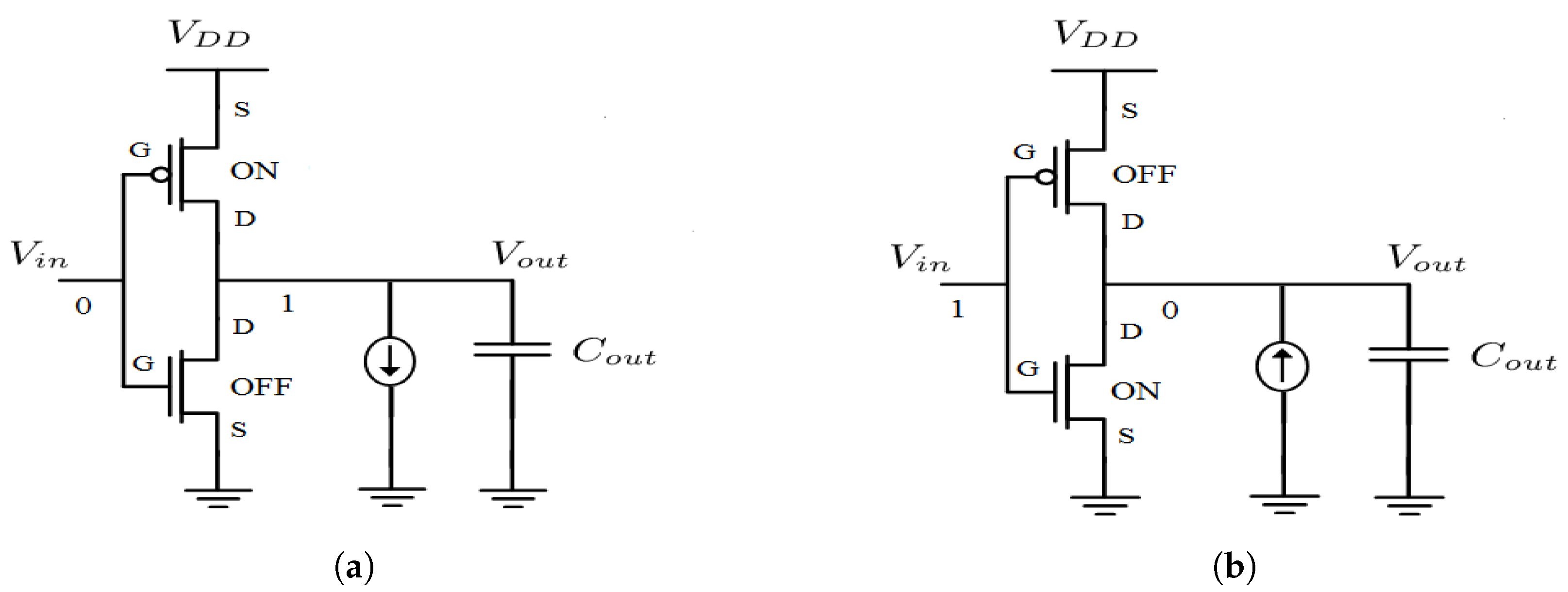
3.2. Transistor Pulse Injection

SETs are mainly caused by high-energy neutrons striking on a transistor’s depletion region. The result is a current pulse that appears at the gate output as a voltage drop. Thus, spice simulations should be performed to model the pulse generation and characterize gate sensitivity. In particular, current pulses are inserted both to NMOS and PMOS transistors for all gate input combinations in order to observe the output pulse. Something that should be underlined is that particle strikes are simulated differently depending on the transistor type they occur. In particular, a fault occurred on a NMOS is simulated with a current pulse injected into the drain and extracted from the body of the transistor, whereas on a PMOS the current pulse enters the body and exits from the drain (Figure 1).
The critical charge required to change the logic state of a gate was significantly decreased due to the technology downscaling. Therefore, electron-hole pairs generated by a particle, which hits a sensitive transistor, can change the gate logic state. However, the emergence of a transient pulse at the gate’s output depends on whether a high-energy particle affects a sensitive region. The aforementioned spice simulation analysis, for all input combinations, shows that sensitive regions are the off transistors [26,27,33].

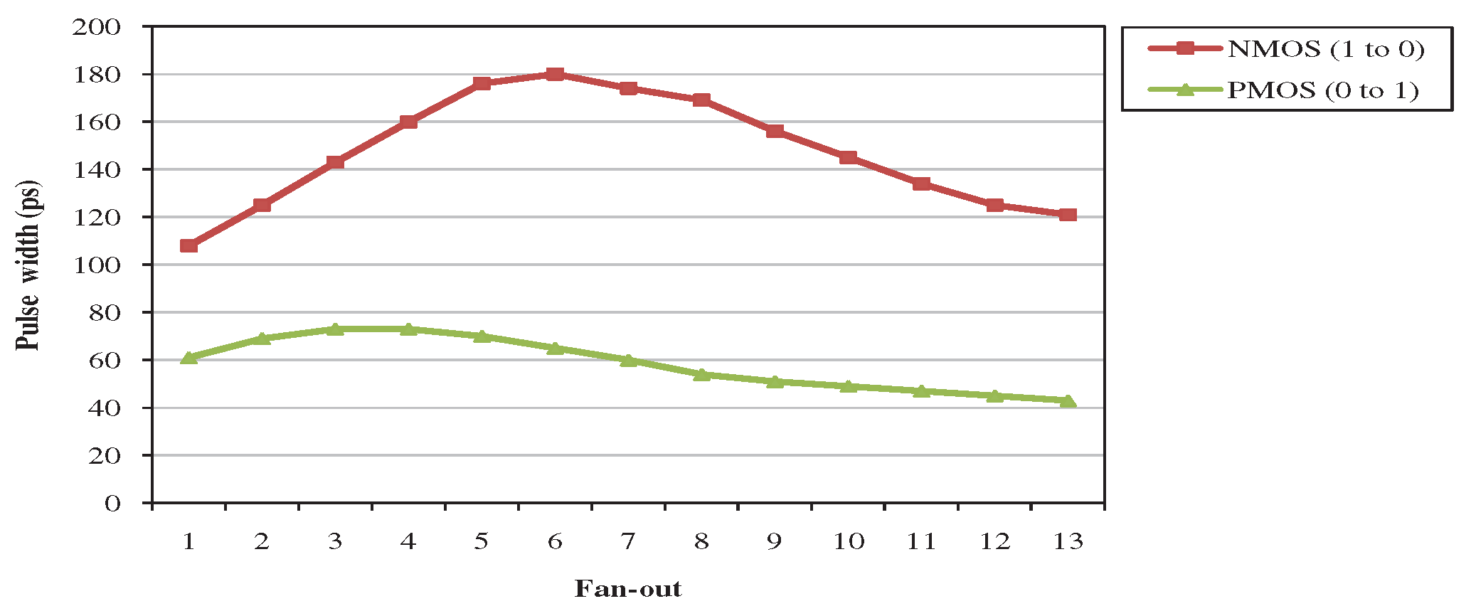
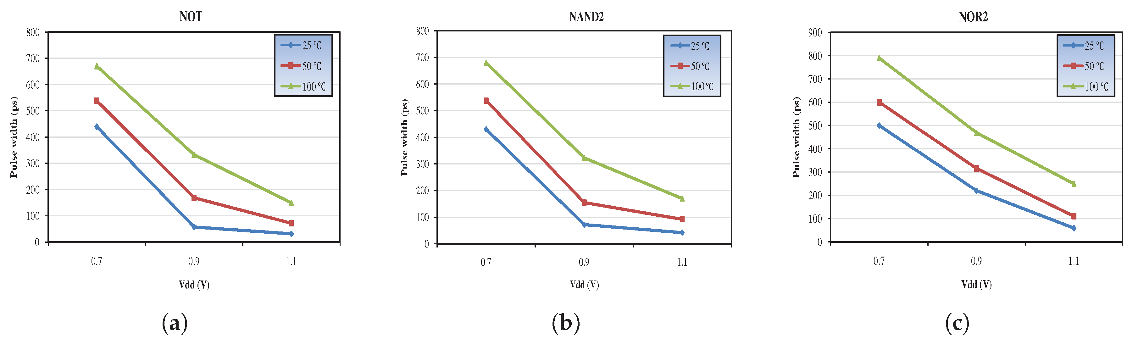
3.3. SET Pulse Characterization

The voltage at the gate output affected by a particle strike depends, primarily, on the energy of the particle and the collected charge, which is determined by the parameters of the injected current pulse. However, the size of the transistor, the output capacitance, the supply voltage as well as temperature, are critical factors for the SET pulse width. Several spice simulations characterized the generated SET pulse under different cases.
First, it was examined the influence of the number of fan-out and, thus, the capacitive load on SET pulse width. Figure 2 shows the pulse widths at the output of a NOT gate for increasing fan-out with identical gates while a current pulse is injected on NMOS and PMOS transistor.
We notice that for less fan-out even though the capacitance increases, the pulse width of the output voltage increases. This is explained from the fact that the injection node needs more time to recharge. On the other hand, the generated pulses tend to have smaller width when fan-out exceeds a threshold. From Figure 2 we can see that this happens for fan-out 6 when NMOS is affected and fan-out 4 when PMOS is affected, since the injected charge is not great enough to change the output voltage to the opposite power trail. Also, the pulse width from a particle strike that flips the output from logic 1 to logic 0 is greater compared to the opposite case. The transconductance coefficient is always greater for NMOS than PMOS, but in the particular implementation the width of the PMOS was not much larger than NMOS (so that the gates were not symmetrical) and, thus, the NMOS current is greater than PMOS current, which justifies the shorter width of the pulse.
Furthermore, the influence of operating voltage and temperature on the SET pulse width was investigated through several simulations. Figure 3 demonstrates the pulse widths of three gates (NOT, NAND2, and NOR2) taking into account different values of the aforementioned factors. In particular, decreasing the operating voltage, which contributes to the reduction of circuit power consumption, results in increased SET pulse widths for the examined logic gates. Furthermore, the elevating temperatures ( 25 ° C, 50 ° C and 100 ° C) show a similar impact on gate sensitivity, which means that under these circumstances, ICs become more susceptible to radiation-induced faults.

3.4. Propagation and Verification Framework

SET characterization is crucial, since glitches with substantial widths may contribute significantly to SER. However, except for that, the analysis of their propagation is equally decisive in order to obtain an accurate SER estimation. Once a transient glitch is generated by a particle hit, it propagates through the following gates and may reach a memory element, if its width is sufficient enough. As mentioned, SET propagation is determined by the strength of the particle and, as a result, by the glitch amplitude and width, and the gates that belong to the corresponding propagation cone, since each one of them has different nodal capacitance affected by parasitic delay and fan-out [36].
For SER verification a script is used, parsing the ISCAS’ 89 spice netlists, to insert current pulses on random transistor nodes and at random time moments within the clock period. Subsequently, the propagation of the generated pulses is examined, whereas an adequate number of simulations are made so as to obtain an accurate result. For all the primary input combinations of the circuit we observe which of the pulses are latched by at least one flip-flop (FF). For this purpose setup and hold time values of the FF are used so as to determine the time interval that glitches can be latched in a clock period. In particular, if a transient fault arrives at a FF within this interval (determined by setup and hold time with respect to the rising edge of the clock pulse), as Figure 4a shows, it is latched, resulting in invalid output (until the next clock edge recovers the right signal), otherwise it is not latched and the FF output remains stable (Figure 4b).

4. Proposed Methodology for SER Estimation

In this section, we present the main aspects of the SER estimation framework, which is based on Monte-Carlo simulations, as this technique provides more accurate results compared to other probabilistic methods (despite being more time-consuming). Emphasis is placed upon the modeling of the three masking phenomena that affect the probability of a TF to become a soft error, and SEMTs.

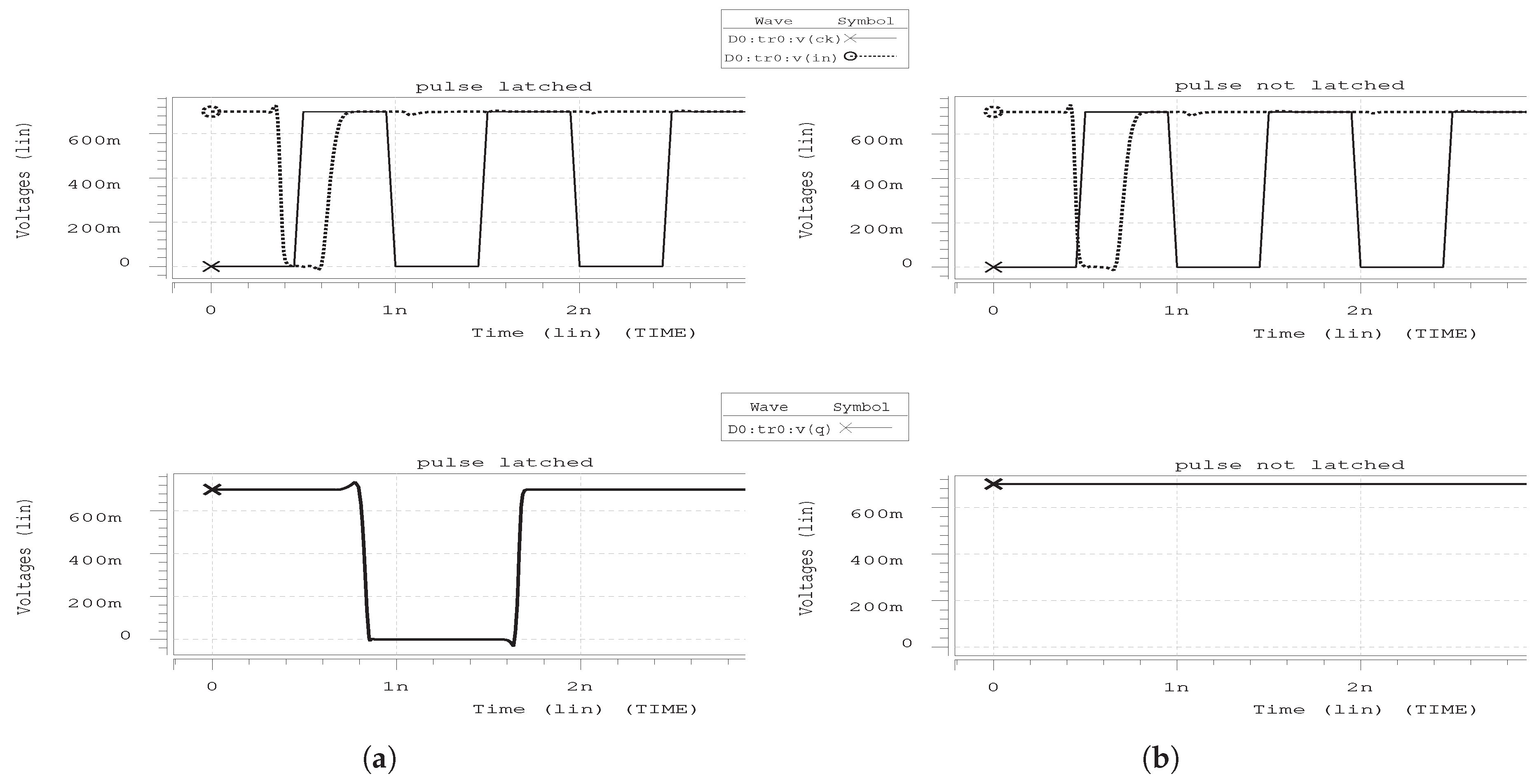
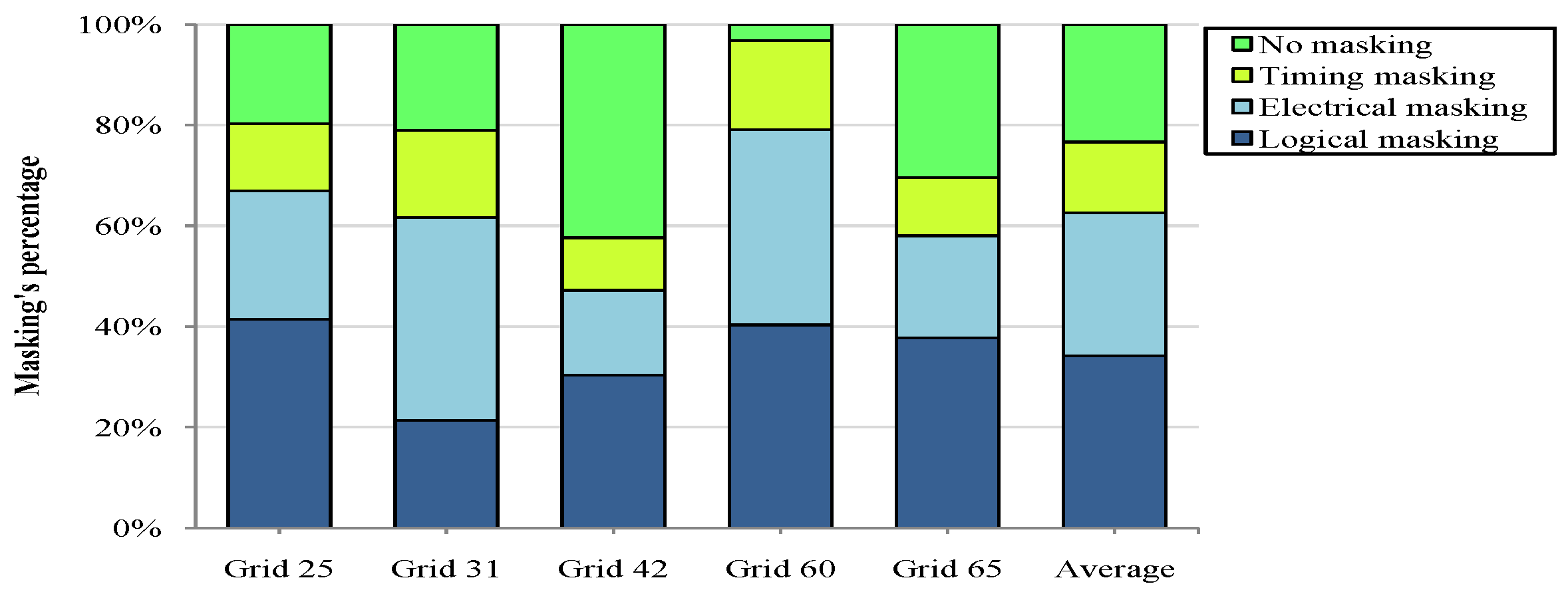
4.1. Masking Mechanisms

A primary part of a SER estimation in combinational logic is the integration of the three mechanisms that prevent SETs from propagating through the circuits and, subsequently, resulting in soft errors [20]. Logical masking is the first factor, which occurs when the glitch propagation is prevented due to an on-path gate, whose output value is controlled by one or more input values. For instance, if an AND gate’s input has a logic value 0 its output will always be logic 0 regardless of the other input values. Thus, every glitch that arrives on any other input will, eventually, be masked. The second, i.e., electrical masking, prevents a TF from reaching the memory elements and, thus, becoming a soft error. The generated pulses are electrically masked due to the electrical properties of the cells they propagate through, since they are attenuated after each pass. For the propagation of the pulse a simple linear function, which depends on the gate delay, is used. A slow gate has a greater contribution to electrical masking than a fast. The last factor, which contributes to the elimination of such disturbances is timing masking, and is associated with the memory elements and their latching window, which is the time interval, determined by the setup and hold time, such that the input signal should be stable to be reliably latched. Therefore, a TF that reaches a FF outside of the latching window becomes masked.

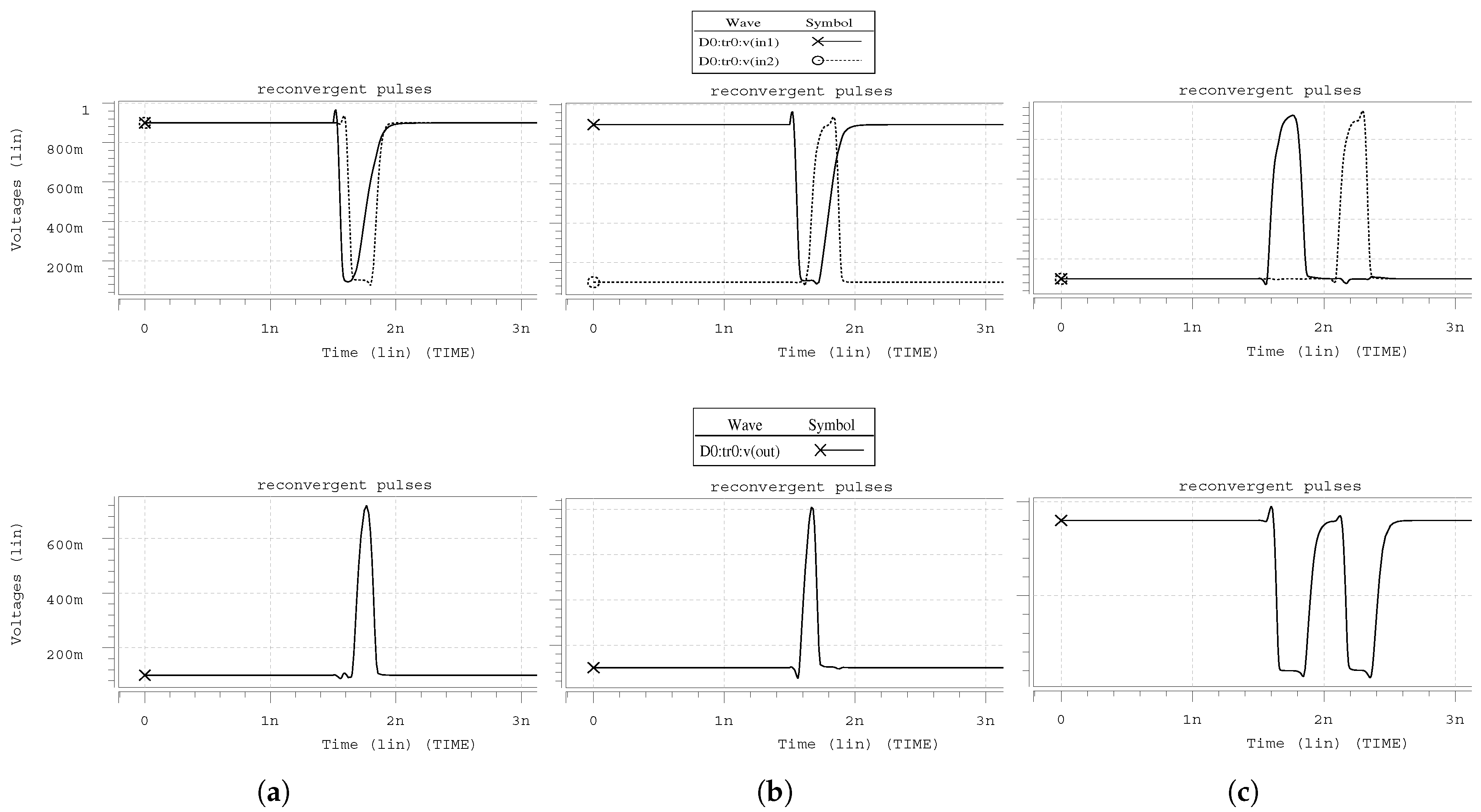
4.2. Reconvergent Transient Faults

A significant factor, which affects the fault propagation, is the examination of reconvergent pulses. This tool takes into account TFs following multiple paths that may reconverge at a subsequent gate. Thus, when two or more pulses of the same TF reconverge at a cell having the same direction (Figure 5a), the output pulse is approximately equal (due to the different rise and fall times) to the overlapping period. On the other hand, as for the overlapping pulses with opposite direction, the resulting pulse at the gate output depends on its type and controlling value. Presenting the simulation of such a case for NOR2 gate, its controlling value is logic 1 and the output pulse equals to the period between the moment that the first pulse falls below half voltage and the moment that the second one rises above half voltage. For the non-overlapping case, as spice simulation shows, both pulses emerge at the output. However, in order to model this case in the proposed framework, for the sake of simplicity, only the greater pulse is taken into consideration.

4.3. Multiple Transient Faults Behavior

MTFs occur when a particle hit affects a circuit area producing glitches on adjacent cells [32]. Therefore, the gates’ output may be changed owing to a corresponding number of sensitive transistors that may be influenced by the hit. The surface affected by a particle hit is depicted by an oval shape, according to the average affected area, which depends on the particle energy [27].
The DEF (Design Exchange Format) files are parsed - for the corresponding ISCAS’ 89 benchmark circuits - which describe the position and placement orientation of each logic cell on the circuit layout. For the identification of the sensitive zones on the circuit layout the GDSII (Graphic Data System) file of each cell was used [30]. These files contain ICs layout information, hence a parser is incorporated into the proposed tool for the extraction of the precise location of the transistor diffusions, and as a result the sensitive regions on the die area. This is a crucial process, since affected cells from a particle strike are considered those whose inactive transistors are located within the oval area [26,30,31].

4.4. Algorithm for SER Εstimation

In order to identify circuit vulnerability to TFs, a topological analysis is presented, based on the division of the circuit layout to several smaller equal parts, called henceforth grids [30]. The number of grids may differ depending on the intended level of granularity. However, there is an upper bound on this number depending on circuit size, since for very small grids the extracted data may be misleading regarding SER. Algorithm 1 summarizes the proposed framework for SER estimation.
Firstly, the DEF and GDSII files of the benchmark under simulation are parsed (lines 1–3) to identify the precise gate positions and their NMOS and PMOS diffusions and register the circuit connectivity. The implemented tool is based on a simple gate-level simulator, and uses the straightforward delay estimation technique of logical effort to determine gate delay, using the FIND_DELAY function.
Algorithm 1: SER Estimation
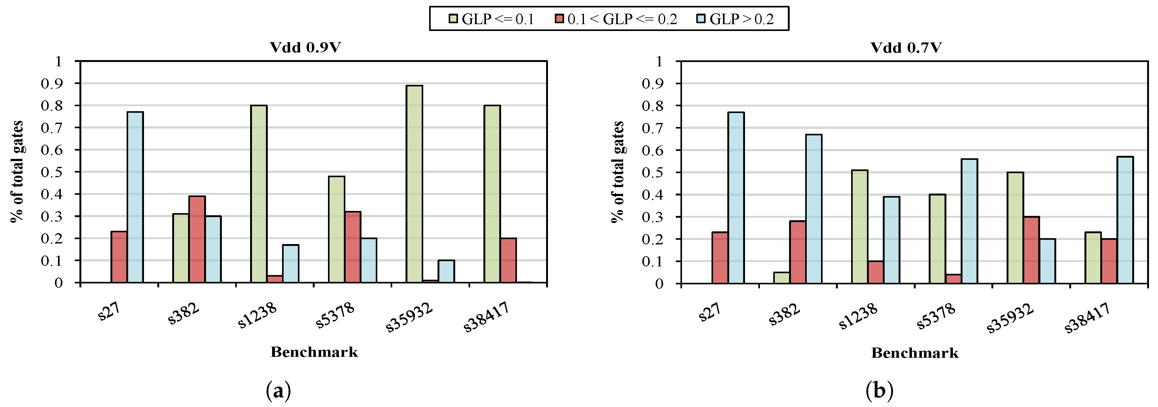
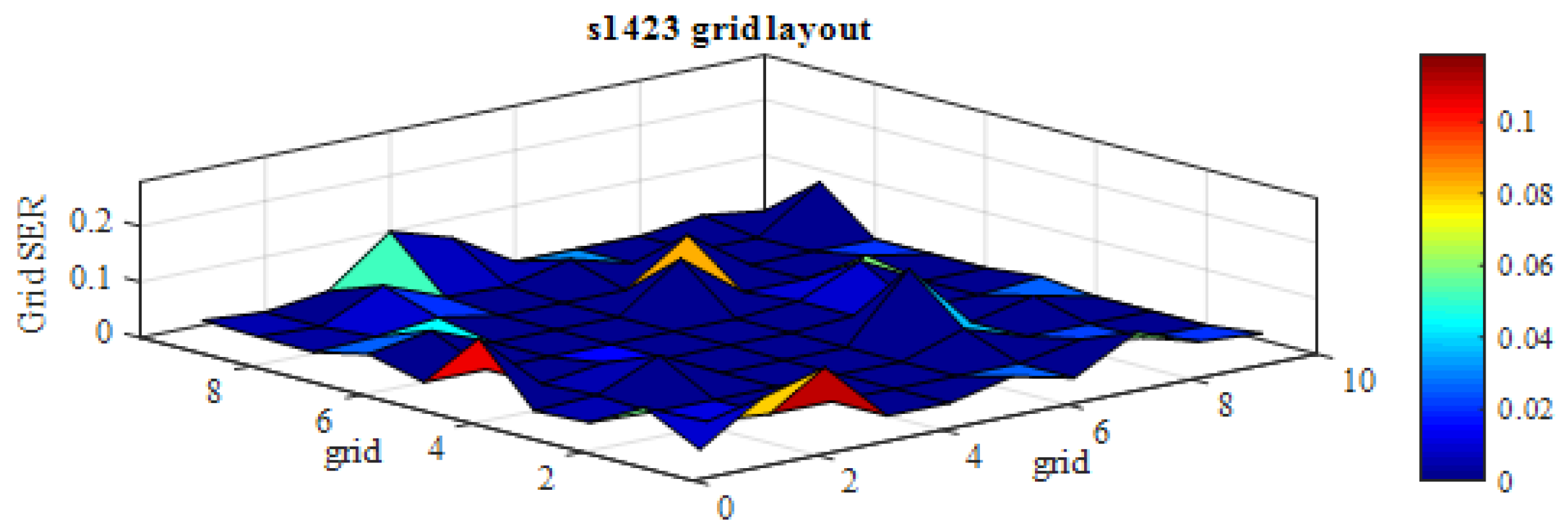
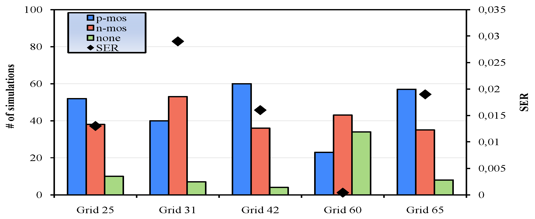
Technologies 08 00005 i001
Next, the circuit is divided into grids (line 6) and for each one, the injection of particle strikes, with different energy at random grid points, generates multiple glitches, via the ERROR_GEN function (lines 9–13). Something that should be highlighted is that the number of grids depends on the size of each circuit. Thus, as circuit complexity increases, more grids are required in order to obtain reliable and comparable results among the different benchmarks. A key point is the treatment of the MTFs propagation, which takes into account all three masking effects and reconvergent pulses. In particular, each pulse originated from a single particle strike, which appears at the output of affected cells, propagates throughout the circuit along with its own logical, electrical and timing masking information. Furthermore, prior to modeling the masking mechanisms, affected transistors are extracted. This is necessary for the identification of the sensitive regions, which takes into consideration gate input values (line 11). Three tables—one per masking effect—for each circuit node are used, in order to examine each error separately and determine those that will be captured by the memory elements. Their size changes dynamically and depends on the number of MTFs generated from a particle strike. In particular, error_state (line 17) is used for logical, whereas error_width (line 21) and error_time (line 24) are used for the electrical and timing masking mechanisms respectively.
To estimate the total latching probability per simulation, the masking effects information is employed, checking if (i) the FF input is affected by particle strike glitches, i.e., if they are not logically masked, (ii) the glitch pulse width is wide enough to actually affect the FF input, and (iii) the pulse arrives within the latching window. All these three checks are performed by the TOTAL_LATCHING_PROB function (line 28). Lastly, in OVERALL_SER function (line 31), the final probability, which represents the circuit SER, is computed considering the latching probabilities per simulation.
SER is usually expressed in Failures In Time (FIT), which is equivalent to the number of failures per one billion hours. This metric is widely used in semiconductor industry due to its efficacy in ICs susceptibility evaluation. As soon as the probabilistic SER is estimated from Algorithm 1, we are able to obtain SER in terms of FIT as:
S E R F I T = F × A × S E R p r o b
where F is the neutron flux, A is the area of the circuit under test, which is exposed to the flux, and S E R p r o b is the probability of SER as computed already.
It is worth mentioning that for large-scale benchmarks the number of 100,000 iterations, for the different primary input vectors, is applied to obtain accurate results. At the end of the simulation, various results and statistics are extracted to evaluate the vulnerability of the circuit to radiation-induced errors (line 32).

5. Gate Sensitivity

This section presents a methodology to identify the sensitivity of the gates to radiation-induced faults. The motivation behind this analysis is that the knowledge of which gates are more sensitive to soft errors is necessary in the effort to reduce their effects on ICs. However, reducing the SER of a circuit through various hardening approaches comes with additional cost in terms of area, delay and power consumption. In order to confine this overhead it is common to harden the most vulnerable areas of the circuit instead of its entirety. The sensitivity of a logic gate corresponds to its relative contribution to the overall circuit SER and is obtained through several targeted simulations.
Intuitively, in combinational logic, a gate is considered sensitive, when the probability of a generated SET during its propagation from the gate output to a memory element is not negligible. In such a case, the presence of the three masking effects that are able to mitigate a SET is vague. Therefore, the metric of the gate sensitivity is inversely proportional to the masking capability of all the three effects jointly. The Glitch Latching Probability (GLP) of each gate of a circuit is defined as the probability that a transient glitch at the gate output will propagate and, eventually, be latched by at least one memory element. A simplified variation of the aforementioned SER estimation methodology is followed to characterize the gate sensitivity. In particular, particle strikes of different width that correspond to the three examined temperatures are injected on each gate. Also, each one of the strikes is applied on different time moments during the clock period. Subsequently, a sufficient number of simulations are performed using different primary input vectors. Performing these simulations under different parameters, we ensure that masking effects are sufficiently simulated. During the simulation, the generated pulse is subjected to the three masking effects as it propagates through the circuit. The probability that all these faults are captured, by at least one sequential element, is obtained, assigning a sensitivity value to each gate, which is computed as follows,
G L P = 1 n i = 1 n l a t c h e d _ g l i t c h ( i )
where n is the total number of simulations and it equals the product n = l × e × t where l is the number of the different primary input vectors for the simulation of logical masking, e is the number of the different width pulses that are used, t is the number of the different constant times that errors occur within the clock period and l a t c h e d _ g l i t c h equals one when a fault is latched by at least one memory element; otherwise is zero.
The large number of simulations, due to the different parameters used, as well as the complexity of the large-scale benchmarks, renders this process time-consuming, yet it provides a quite accurate assessment of the relative sensitivity among the gates of a given design. A basic difference with the main SER estimation methodology is that we neglect SEMTs, as the process for sensitivity identification targets each gate separately. If SEMT analysis was considered, the sensitivity results would involve the gate adjacency, which is not the case. On the contrary, for the selective hardening of the most susceptible gates only the sensitivity of the gate itself should be taken into account.
Figure 6 demonstrates the gate sensitivity of some circuits for different supply voltages regarding the GLP values of the gates. In particular, two GLP thresholds are set to distribute the gates in three sensitivity levels. For supply voltage at 0.7 V more than half of the gates, for the most of the designs, exceed the threshold of 0.2, i.e., GLP > 0.2 , which means that a particle occurred on any of these is more likely to result in a soft error. On the other hand, when supply voltage is at 0.9 V and, thus, the generated pulse width is smaller most of the gates do not exceed the lowest threshold, i.e., GLP 0.1 . However, for the s27 design the distribution is similar (all the gates have GLP > 0.1 ) and this is explained from the fact that almost all the gates are close to FFs (due to its size) and the probability that a glitch, regardless of its width, becomes masked is great. In conclusion, the advantage that offers this method is that the gate sensitivity values may be exploited in order to harden the most vulnerable of them to succeed SER reduction.

6. Experimental Results

The proposed tool is implemented in C and all the experiments are performed on a Linux workstation with an Intel Core i7-3770 processor @3.4GHz and 8GB of main memory and are conducted on a set of ISCAS’ 89 benchmark circuits, synthesized with respect to 45nm Nangate Open Cell Library [37].
Figure 7 shows the susceptibility of the s1423 benchmark presenting the SER estimation for each grid. Some areas seem to be more vulnerable than others, making it possible for the designers to reconsider and improve the placement process in order to mitigate SER.
Figure 8 presents in what degree the masking effects impact on SER for some grids of the s15850 circuit. In particular, logical and electrical masking have a greater effect on SER mitigation than timing. Moreover, grid 60 is expected to be less vulnerable compared to grid 42, since almost all errors are completely masked. SER estimation depends on the affected transistors type as well. When a particle strikes an inactive NMOS transistor the generated pulse is greater, as explained in Section 3. Thus, the results presented in Figure 9, in combination with those of Figure 8 give a more detailed view of the grids susceptibility.
In particular, Figure 9 presents in how many of the 100 simulations, i.e., particle strikes, the number of affected PMOS exceed the corresponding number of NMOS transistors and vice versa. Furthermore, it shows the number of simulations that particle hits have no impact on the circuit as well as the SER of each grid. The SER of grid 31 is greater than grid’s 25 even though the corresponding percentages of the errors that are not masked are nearly equal. This is explained since the affected NMOS transistors for the former grid are greater than the latter.
The modeling of SET pulse width is a key factor as it is a function of operating temperature [15]. Increasing the temperature, pulse widths become more intense leading, as a result, to a greater SER. Figure 10 shows the estimated SER at three different temperatures. Increasing the temperature for the same technology of 45-nm, the generated pulses become larger, as characterization process shows, and this explains the fact that at the temperature of 100 ° C SER is greater in comparison with the other two cases.
Table 1 reports SER estimation for ISCAS’ 89 benchmarks along with the execution time. SER is expressed as probability and FIT as well.
For FIT calculation, the flux of 20.329 n e u t r o n s / c m 2 h is considered, which is the neutron flux at sea level at New York City [3], whereas temperature remains stable at 25 ° C and supply voltage at 0.7 V for all the experiments. SER results for two types of simulations are presented. The first considers explicitly the occurence of SETs, while in contrast, the second allows for the occurence of SEMTs. We notice that when SEMTs are considered, the SER increases for all the benchmarks. As regards the failure rate, it decreases as benchmark complexity increases, since for smaller circuits SETs are more probable to be latched by memory elements. On the other hand, the SER in terms of FIT is estimated taking into consideration the circuit area; hence its value is elevated, especially for the large-scale benchmarks. Finally, the verification with HSPICE, which gives a maximum deviation of 10%, is made for small-scale benchmarks since it is extremely time-consuming as complexity increases.

7. Conclusions

In this paper, we presented a tool for SER estimation regarding multiple transient faults, whose propagation is examined separately. The use of placement information and the results of the characterization process with HSPICE, which gave an overview of the pulse width for different conditions, were taken into account in the proposed framework, in order to achieve an accurate SER estimation. Furthermore, the GLP metric quantifies the gate sensitivity to radiation by determining the probability of a generated glitch to lead to a soft error. Therefore, the outcome of our experiments, regarding both SER and gate sensitivity for voltage, temperature and output capacitance variations, can be exploited in industry, in an effort to further improve error-resistance of modern ICs.

Author Contributions

Conceptualization, G.I.P. and P.T.; data curation, G.I.P. and P.T.; funding acquisition, N.E., G.D. and G.I.S.; investigation, G.I.P. and P.T.; methodology, G.I.P. and P.T.; preparation, G.I.P. and P.T.; project administration, N.E., G.D. and G.I.S.; software, G.I.P. and P.T.; supervision, N.E., G.D. and G.I.S.; validation, G.I.P. and P.T.; writing–original draft, G.I.P. and P.T.; writing–review and editing, G.I.P.; P.T.; N.E.; G.D.; G.I.S. All authors have read and agreed to the published version of the manuscript.

Funding

This research received no external funding.

Conflicts of Interest

The authors declare no conflict of interest.

Abbreviations

The following abbreviations are used in this manuscript:
CMOSComplementary Metal–Oxide–Semiconductor
SERSoft Error Rate
VLSIVery Large-Scale Integration
ICIntegrated Circuit
SETSingle Event Transient
SEMTSingle Event Multiple Transient
TFTransient Fault
MTFMultiple Transient Fault
FFFlip-Flop
DEFDesign Exchange Format
GDSIIGraphic Database System
GLPGlitch Latching Probability

References

  1. Campos, A.; Espinosa, G.; Torres Jacome, A.; Tlelo-Cuautle, E. On the Prediction of the Threshold Voltage Degradation in CMOS Technology Due to Bias-Temperature Instability. Electronics 2019, 7, 427. [Google Scholar] [CrossRef] [Green Version]
  2. May, T.C.; Woods, M.H. Alpha-particle-induced soft errors in dynamic memories. IEEE Trans. Electron Devices 1979, 26, 2–9. [Google Scholar] [CrossRef]
  3. Ziegler, J.F. Terrestrial cosmic rays. IBM J. Res. Dev. 1996, 40, 19–39. [Google Scholar] [CrossRef]
  4. Hazucha, P.; Svensson, C. Impact of CMOS technology scaling on the atmospheric neutron soft error rate. IEEE Trans. Nucl. Sci. 2000, 47, 2586–2594. [Google Scholar] [CrossRef]
  5. Seifert, N.; Slankard, P.; Kirsch, M.; Narasimham, B.; Zia, V.; Brookreson, C.; Vo, A.; Mitra, S.; Gill, B.; Maiz, J. Radiation-induced soft error rates of advanced CMOS bulk devices. In Proceedings of the IEEE International Reliability Physics Symposium (IRPS), San Jose, CA, USA, 26–30 March 2006; pp. 217–225. [Google Scholar]
  6. Chandra, V.; Aitken, R. Impact of Technology and Voltage Scaling on the Soft Error Susceptibility in Nanoscale CMOS. In Proceedings of the IEEE International Symposium on Defect and Fault Tolerance of VLSI Systems, Boston, MA, USA, 1–3 October 2008; pp. 114–122. [Google Scholar]
  7. Carbajal-Gómez, V.; Tlelo-Cuautle, E.; Munoz-Pacheco, J.M.; De La Fraga, L.; Sanchez-Lopez, C.; Fernandez-Fernandez, F. Optimization and CMOS design of chaotic oscillators robust to PVT variations. Integration 2019, 65, 32–42. [Google Scholar] [CrossRef]
  8. HSPICE® User Guide: Simulation and Analysis, Version b-2008.09. 2008. Available online: https://cseweb.ucsd.edu/classes/wi10/cse241a/assign/hspice_sa.pdf (accessed on 6 January 2020).
  9. Tlelo-Coyotecatl, E.; Diaz-Sanchez, A.; Rocha-Pérez, J.; Vazquez-Gonzalez, J.L.; Sánchez-Gaspariano, L.; Tlelo-Cuautle, E. Enhancing Q-Factor in a Biquadratic Bandpass Filter Implemented with Opamps. Technologies 2019, 7, 64. [Google Scholar] [CrossRef] [Green Version]
  10. Paliaroutis, G.I.; Tsoumanis, P.; Evmorfopoulos, N.; Dimitriou, G.; Stamoulis, G.I. Multiple Transient Faults in Combinational Logic with Placement Considerations. In Proceedings of the 8th International Conference on Modern Circuits and Systems Technologies on Electronics and Communications (MOCAST), Thessaloniki, Greece, 13–15 May 2019; pp. 1–4. [Google Scholar]
  11. Gadlage, M.J.; Ahlbin, J.R.; Ramachandran, V.; Gouker, P.; Dinkins, C.A.; Bhuva, B.L.; Narasimham, B.; Schrimpf, R.D.; McCurdy, M.W.; Alles, M.L.; et al. Temperature Dependence of Digital Single-Event Transients in Bulk and Fully-Depleted SOI Technologies. IEEE Trans. Nucl. Sci. 2009, 56, 3115–3121. [Google Scholar] [CrossRef]
  12. Glorieux, M.; Evans, A.; Ferlet-Cavrois, V.; Boatella-Polo, C.; Alexandrescu, D.; Clerc, S.; Gasiot, G.; Roche, P. Detailed SET Measurement and Characterization of a 65nm Bulk Technology. IEEE Trans. Nucl. Sci. 2016, 64, 81–88. [Google Scholar] [CrossRef]
  13. Dixit, A.; Wood, A. The impact of new technology on soft error rates. In Proceedings of the International Reliability Physics Symposium, Monterey, CA, USA, 10–14 April 2011; pp. 5B.4.1–5B.4.7. [Google Scholar]
  14. Cha, H.; Patel, J.H. A logic-level model for α-particle hits in CMOS circuits. In Proceedings of the IEEE International Conference on Computer Design ICCD’93, Cambridge, MA, USA, 3–6 October 1993; pp. 538–542. [Google Scholar]
  15. Xu, J.; Guo, Y.; Song, R.; Liang, B.; Chi, Y. Supply Voltage and Temperature Dependence of Single-Event Transient in 28-nm FDSOI MOSFETs. Symmetry 2019, 11, 793. [Google Scholar] [CrossRef] [Green Version]
  16. Wang, F.; Xie, Y. Soft Error Rate Analysis for Combinational Logic Using an Accurate Electrical Masking Model. IEEE Trans. Depend. Sec. Comp. 2011, 8, 137–146. [Google Scholar] [CrossRef]
  17. Rao, R.R.; Chopra, K.; Blaauw, D.T.; Sylvester, D.M. Computing the Soft Error Rate of a Combinational Logic Circuit Using Parameterized Descriptors. IEEE Trans. Comput. Aided Des. Integr. Circuits Syst. 2007, 26, 468–479. [Google Scholar] [CrossRef]
  18. Zhang, M.; ShanbhagHazucha, N.R. Soft-Error-Rate-Analysis (SERA) methodology. IEEE Trans. Comput. Aided Des. Integr. Circuits Syst. 2006, 25, 2140–2155. [Google Scholar] [CrossRef]
  19. Anglada, M.; Canal, R.; Aragón, J.L.; González, A. MASkIt: Soft error rate estimation for combinational circuits. In Proceedings of the IEEE 34th International Conference on Computer Design (ICCD), Scottsdale, AZ, USA, 2–5 October 2016; pp. 614–621. [Google Scholar]
  20. Wang, F.; Agrawal, V.D. Soft error rate determination for nanoscale sequential logic. In Proceedings of the 11th International Symposium on Quality Electronic Design (ISQED), San Jose, CA, USA, 22–24 March 2010; pp. 225–230. [Google Scholar]
  21. Chang, A.C.-C.; Huang, R.H.; Wen, C.H. CASSER: A closed-form analysis framework for statistical soft error rate. IEEE Trans. Very Large Scale Integr. Syst. 2013, 21, 1837–1848. [Google Scholar] [CrossRef]
  22. Kiddie, B.T.; Robinson, W.H.; Limbrick, D.B. Single-Event Multiple-Transients (SEMT): Circuit characterization and analysis. In Proceedings of the IEEE Workshop Silicon Errors in Logic-System Effects (SELSE), Palo Alto, CA, USA, 26–27 March 2013. [Google Scholar]
  23. Evans, A.; Glorieux, M.; Alexandrescu, D.; Polo, C.B.; Ferlet-Cavrois, V. Single event multiple transient (SEMT) measurements in 65 nm bulk technology. In Proceedings of the 16th European Conference on Radiation and Its Effects on Components and Systems, Bremen, Germany, 19–23 September 2016; pp. 1–6. [Google Scholar]
  24. Rossi, D.; Omana, M.; Toma, F.; Metra, C. Multiple transient faults in logic: An issue for next generation ICs? In Proceedings of the IEEE International Symposium on Defect and Fault Tolerance in VLSI Systems, Monterey, CA, USA, 3–5 October 2005; pp. 352–360. [Google Scholar]
  25. Nanditha, P.R.; Sarik, S.; Desai, M.P. On the likelihood of multiple bit upsets in logic circuits. arXiv 2014, arXiv:1401.1003. [Google Scholar]
  26. Huang, H.; Wen, C.H.-P. Layout-Based soft error rate estimation framework considering multiple transient faults—From device to circuit level. IEEE Trans. Comput. Aided Des. Integr. Circuits Syst. 2016, 35, 586–597. [Google Scholar] [CrossRef]
  27. Ebrahimi, M.; Asadi, H.; Tahoori, M.B. A layout-based approach for multiple event transient analysis. In Proceedings of the 50th ACM/EDAC/IEEE Design Automation Conference (DAC), Austin, TX, USA, 29 May–7 June 2013; pp. 1–6. [Google Scholar]
  28. Miskov-Zivanov, N.; Marculescu, D. Multiple transient faults in combinational and sequential circuits: A systematic approach. IEEE Trans. Comput. Aided Des. Integr. Circuits Syst. 2010, 29, 1614–1627. [Google Scholar] [CrossRef]
  29. Fazeli, M.; Ahmadian, S.N.; Miremadi, S.G.; Asadi, H.; Tahoori, M.B. Soft error rate estimation of digital circuits in the presence of Multiple Event Transients (METs). In Proceedings of the Design, Automation & Test in Europe Conference & Exhibition (DATE), Grenoble, France, 14–18 March 2011; pp. 1–6. [Google Scholar]
  30. Paliaroutis, G.I.; Tsoumanis, P.; Evmorfopoulos, N.; Dimitriou, G.; Stamoulis, G.I. A placement-aware soft error rate estimation of combinational circuits for multiple transient faults in CMOS technology. In Proceedings of the IEEE International Symposium on Defect and Fault Tolerance in VLSI and Nanotechnology Systems, Chicago, IL, USA, 8–10 October 2018; pp. 1–6. [Google Scholar]
  31. Du, Y.; Chen, S. A novel layout-based single event transient injection approach to evaluate the soft error rate of large combinational circuits in Complimentary Metal-Oxide-Semiconductor bulk technology. IEEE Trans. Reliab. 2016, 65, 248–255. [Google Scholar] [CrossRef]
  32. Li, J.; Draper, J. Accelerated Soft-Error-Rate (SER) estimation for combinational and sequential circuits. ACM Trans. Des. Autom. Electr. Syst. 2017, 22, 57. [Google Scholar] [CrossRef]
  33. Cao, X.; Xiao, L.; Li, J.; Zhang, R.; Liu, S.; Wang, J. A layout-based soft error vulnerability estimation approach for combinational circuits considering Single Event Multiple Transients (SEMTs). IEEE Trans. Comput. Aided Des. Integr. Circuits Syst. 2018, 38, 1109–1122. [Google Scholar] [CrossRef]
  34. Messenger, G.C. Collection of Charge on Junction Nodes from Ion Tracks. IEEE Trans. Nucl. Sci. 1982, 29, 2024–2031. [Google Scholar] [CrossRef]
  35. Srinivasan, G.R.; Murley, P.C.; Tang, H.K. Accurate, predictive modeling of soft error rate due to cosmic rays and chip alpha radiation. In Proceedings of the IEEE International Reliability Physics Symposium, San Jose, CA, USA, 11–14 April 1994; pp. 12–16. [Google Scholar]
  36. Naseer, R.; Draper, J.; Boulghassoul, Y.; DasGupta, S.; Witulski, A. Critical charge and set pulse widths for combinational logic in commercial 90nm cmos technology. In Proceedings of the 17th ACM Great Lakes Symposium on VLSI, Stresa, Lago Maggiore, Italy, 11–13 March 2007. [Google Scholar]
  37. Nangate 45nm Open Cell Library, Nangate Inc. 2009. Available online: http://www.nangate.com/ (accessed on 6 January 2020).
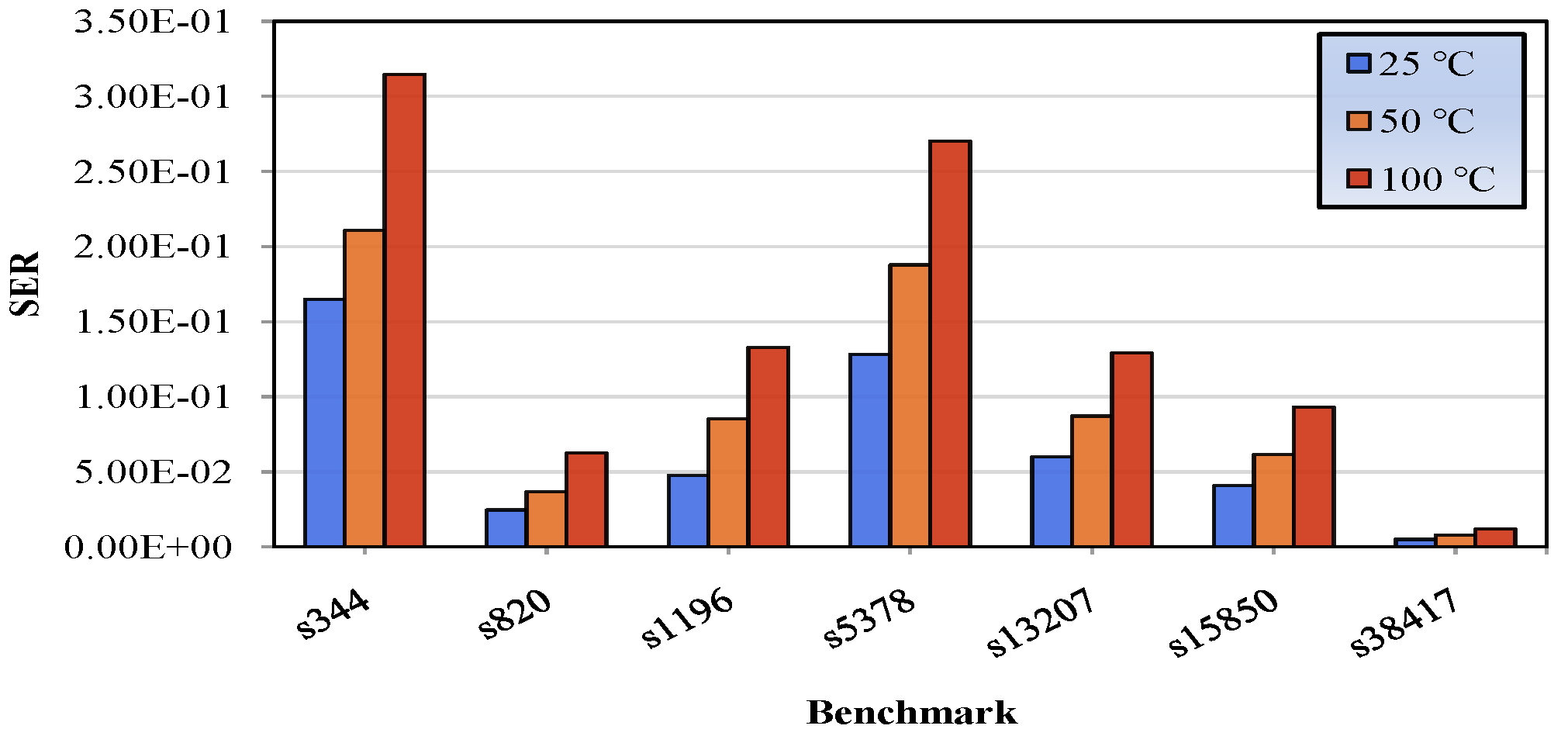
Figure 1. Modeling of the particle strike on an inverter via the current pulse when (a) it occurs on NMOS transistor and (b) on PMOS transistor.
Technologies 08 00005 g001
Figure 2. Pulse widths for various fan-out when NMOS and PMOS is affected.
Technologies 08 00005 g002
Figure 3. Pulse widths for different supply voltages and temperatures of (a) NOT, (b) NAND2 and (c) NOR2 gates.
Technologies 08 00005 g003
Figure 4. Transient pulse when (a) it is latched and (b) it is not latched.
Technologies 08 00005 g004
Figure 5. Output pulses for (a) same direction, (b) different direction and (c) non-overlapping input reconvergent pulses.
Technologies 08 00005 g005
Figure 6. Distribution of gate sensitivity for 6 benchmarks with supply voltage (a) 0.9V and (b) 0.7V.
Technologies 08 00005 g006
Figure 7. Grids SER for s1423 benchmark.
Technologies 08 00005 g007
Figure 8. Particular grids of s15850 and the percentage of the injected errors that become logically, electrically and timingly masked.
Technologies 08 00005 g008
Figure 9. Number of affected transistors for 100 simulations for some grids of s15850 with the corresponding SER values.
Technologies 08 00005 g009
Figure 10. SER of a set of benchmarks for three different temperatures.
Technologies 08 00005 g010
Table 1. SER evaluation results obtained from the proposed tool for ISCAS’ 89 benchmarks. The number of nodes, primary inputs, gates and D-type FFs indicate the benchmarks’ complexity, SETs denotes the consideration of single transient faults, SEMTs denotes the consideration of multiple transient faults, Fail. Rate is the SER probability, FIT is the SER in terms of FIT, whereas Ex. Time denotes the average execution time of the analyses.
BenchmarkNodesInputsGatesFFsSEREx. Time
SETsSEMTs
Fail. RateFITFail. RateFIT
s271741330.2218304.95 × 10−60.2789876.22 × 10−6 < 1 s
s2981693166140.1055484.28 × 10−60.1197064.86 × 10−6 < 1 s
s3442409231150.1518767.65 × 10−60.1650338.32 × 10−6 < 1 s
s3492249215150.1474167.43 × 10−60.1515637.63 × 10−6 < 1 s
s3821963193210.1478838.84 × 10−60.2192131.31 × 10−5 < 1 s
s4002033200210.1524269.21 × 10−60.1970171.19 × 10−5 < 1 s
s42025219233160.1186417.41 × 10−60.1552589.70 × 10−6 < 1 s
s5262803277210.1587641.15 × 10−50.2217931.61 × 10−51 s
s64151735482190.0523954.85 × 10−60.0687856.36 × 10−62 s
s71353935504190.0468824.45 × 10−60.0600035.70 × 10−62 s
s8204431842550.0170641.52 × 10−60.0246292.19 × 10−62 s
s95349616480290.2009702.23 × 10−50.1548861.71 × 10−57 s
s119676214748180.0367765.02 × 10−60.0475496.48 × 10−64 s
s123876814754180.0369945.12 × 10−60.0517797.17 × 10−64 s
s1423100817991740.0259366.60 × 10−50.0345678.08 × 10−510 s
s148812118120360.0092521.68 × 10−60.0189313.44 × 10−64 s
s537830533530181790.1048127.20 × 10−50.1283008.82 × 10−5 1.7 m
s923470021969832280.0432965.45 × 10−50.0526996.55 × 10−5 6.3 m
s1320796083195776690.0514291.10 × 10−40.0597801.26 × 10−4 7.4 m
s1585012,1151412,1015970.0312777.32 × 10−50.0406799.53 × 10−5 12.2 m
s3593221,2783521,24317280.0509042.70 × 10−40.0661153.51 × 10−458 m
s3841724,8742823,81516360.0387411.08 × 10−20.0516371.44 × 10−210 h
s3858421,4073820,67914260.0304398.12 × 10−30.0426581.12 × 10−27 h

