Article

UV-Responsive Screen-Printed Porous ZnO Nanostructures on Office Paper for Sustainable and Foldable Electronics

i3N/CENIMAT, Department of Materials Science, Faculty of Science and Technology, Campus de Caparica, Universidade NOVA de Lisboa and CEMOP/UNINOVA, 2829-516 Caparica, Portugal
*
Authors to whom correspondence should be addressed.
Submission received: 30 June 2021 / Revised: 19 July 2021 / Accepted: 20 July 2021 / Published: 24 July 2021
(This article belongs to the Collection Sustainable Metal Oxide Materials for Sensing Applications)

Abstract

:
The fabrication of low-cost, flexible, and recyclable electronic devices has been the focus of many research groups, particularly for integration in wearable technology and the Internet of Things (IoT). In this work, porous zinc oxide (ZnO) nanostructures are incorporated as a UV sensing material into the composition of a sustainable water-based screen-printable ink composed of carboxymethyl cellulose (CMC). The formulated ink is used to fabricate flexible and foldable UV sensors on ubiquitous office paper. The screen-printed CMC/ZnO UV sensors operate under low voltage (≤2 V) and reveal a stable response over several on/off cycles of UV light exposure. The devices reach a response current of 1.34 ± 0.15 mA and a rise and fall time of 8.2 ± 1.0 and 22.0 ± 2.3 s, respectively. The responsivity of the sensor is 432 ± 48 mA W−1, which is the highest value reported in the literature for ZnO-based UV sensors on paper substrates. The UV-responsive devices display impressive mechanical endurance under folding, showing a decrease in responsivity of only 21% after being folded 1000 times. Their low-voltage operation and extreme folding stability indicate a bright future for low-cost and sustainable flexible electronics, showing potential for low-power wearable applications and smart packaging.

Graphical Abstract

1. Introduction

Paper is a renewable raw material that has been used by humankind for thousands of years to share and store information. Over the last few decades, many researchers and industries have not been looking at paper for its conventional application of transmitting information, but as a substrate for the development of low-cost, flexible, and recyclable electronic devices that will in a close future find their place in our daily life, thus leading to a revolutionary and sustainable era of electronics [1,2,3,4,5].
Cellulose, known as the most abundant and renewable biopolymer on Earth, is the building block of paper, and therefore responsible for its beneficial features, such as lightweight, low thermal expansion, flexibility/foldability, biodegradability, and recyclability [5]. Paper is also compatible with roll-to-roll (R2R) manufacturing processes, and it is available in several textures, compositions, and coatings [4,6,7].
The idea of using ubiquitous paper substrates as a low-cost, flexible, and robust support for printed electronic applications has already been demonstrated on memory devices [8], chromogenic displays [9,10,11], photovoltaics cells [12], paper-based microfluidic devices [13], and transistors and integrated circuits [14,15,16,17,18,19,20,21]. Inspired by the pioneer work introduced in our research group by Fortunato et al. [22] in 2008, Grey et al. [21] also successfully explored the intrinsic dielectric/electrolytic properties of paper, which was used not only as a substrate but also as an active electronic material to work as the gate dielectric layer in printed/handwritten ZnO transistors.
Paper electronics relies on the development of stable, low-cost, non-toxic, and environmentally friendly printable inks to deposit and pattern functional materials onto paper [23]. Printable inks consist of a combination of functional materials, binders, additives, and solvents, each one impacting the inks’ viscosity, rheology, evaporation rate, and surface tension [23,24]. There is an increasing interest in the development of water-based inks, since water is a cheap and eco-friendly solvent [25]. Cellulose derivatives, such as carboxymethyl cellulose (CMC), have been applied as a biopolymeric binder in the formulation of water-based printable inks [26,27,28].
However, the large surface roughness, high absorption capacity, and porosity in conventional paper speed up lateral spreading of the inks, leading to low-resolution and irregular/deformed printed features, thus compromising their functionality [16,29,30]. These adverse effects can be overcome with the use of inks with a “honey-like” viscosity (0.03–50 Pa s), such as the ones compatible with the screen-printing technique, since they enable the deposition of thicker films while preventing the excessive bleeding and swelling of the cellulose fibers [31]. This printing technique is widely used in printed electronics due to its simple operation, ease of prototyping, no need of complex equipment, fast printing speed (150 m min−1), compatibility with substrates with tailored textures, and versatility of pattern designs (resolution around 30–100 µm) [32,33,34].
From a broad list of functional materials, ZnO is an n-type semiconductor with a wide bandgap of 3.37 eV and high exciton binding energy of 60 meV at room temperature that crystalizes in a hexagonal wurtzite structure [35]. The simple synthesis methods that exist to produce ZnO nanostructures with tailored sizes and morphologies, along with low-temperature processability (<300 °C), chemical and thermal stability, abundant availability, and non-toxic nature, among several other features, makes ZnO one of the most investigated metal semiconductor oxides in a wide range of applications [36,37,38,39,40,41,42,43,44,45]. Among all the existing synthesis methods to obtain ZnO nanostructures, microwave hydrothermal/solvothermal synthesis is particularly interesting due to the high reaction rates that result from the absorption of microwave radiation by the materials. As a result, a homogeneous and fast volumetric heating is obtained during synthesis, which allows the production of ZnO nanostructures in minutes [46,47,48,49,50,51,52].
ZnO nanostructures have been employed before in the development of screen-printable inks for paper electronic applications. In our group, several works have been published reporting the fabrication of screen-printable inks based on cellulose derivatives and commercial ZnO nanoparticles for a variety of applications, such as UV sensors [53,54], field effect transistors [21], and electrolyte-gated transistors [20]. Besides paper electronics, ZnO-based pastes and inks have also been developed for a wide range of applications, including solar cells [55], photoelectrochemical cells [56], gas sensors [57], and light-emitting diodes [58].
ZnO nanostructures with a porous morphology are advantageous for sensing applications, as a high number of pores result in high specific surface areas for the adsorption of molecules, thus enhancing their sensing responsivity [59,60]. Although there are several reports that demonstrate the superior performance of porous ZnO nanostructures in gas sensors [60,61,62,63,64], dye-sensitized solar cells [65], batteries [66], photocatalysis [67,68,69], and biosensing [70], their performance in paper-based UV sensors has not yet been exploited.
Porous ZnO nanostructures can be produced by calcination of layered zinc hydroxide (LZH) materials [68], particularly LZHs intercalated by carbonate ions (LZHC) [66,68,71,72,73]. LZHC nanomaterials can be obtained by hydrothermal synthesis with a plate-like morphology assembled in 3D hierarchical structures and then be converted into porous ZnO nanostructures by calcination at high temperatures while maintaining a similar morphology, as demonstrated in our previous works [67,74].
Within this context, this work reports the fabrication of porous ZnO nanostructures with a plate-like morphology by microwave hydrothermal synthesis of LZHC and its subsequent calcination at 700 °C. The synthesized porous ZnO nanostructures were employed in the formulation of a water-based screen-printable CMC/ZnO composite ink. To the best of our knowledge, this is the first work reporting the incorporation of ZnO nanostructures with a porous morphology in a water-based screen-printable ink. The fabricated ink was integrated into UV sensors built onto office paper. The photonic devices were tested under different applied voltages and UV light intensities, and their mechanical endurance was also investigated. Their UV responsiveness far exceeds the ones reported in the literature when using ZnO nanostructures together with cellulosic materials/substrates, reaching response currents in the mA range when operating under low voltage (2 V).

2. Materials and Methods

2.1. Synthesis and Characterization of Porous ZnO Nanostructures

Following the procedure reported in our previous work [67], porous ZnO nanostructures were synthesized by hydrothermal method assisted by microwave irradiation. Briefly, 0.05 M of zinc nitrate hexahydrate (Zn(NO3)2·6H2O, 98% from Sigma-Aldrich, St. Louis, MO, USA) was first dissolved in deionized water, followed by the addition of urea (CH4N2O, 99.0–100.5% from Sigma-Aldrich, St. Louis, MO, USA) to the aqueous solution in a molar ratio of zinc to urea of 1:5. The synthesis was carried out in a Discovery SP microwave (CEM, Matthews, NC, USA) at 140 °C for 15 min under a power of 100 W. After the synthesis, the resulting white precipitates were washed with deionized water followed by isopropanol and centrifuged at 4000 rpm for 5 min each. This washing process was repeated three times. The powders were dried in air at room temperature and then calcinated in a muffle furnace (Nabertherm GmbH, Lilienthal, Germany) at 700 °C for 2 h in air at a heating rate of 250 °C h−1.
The morphology of the ZnO nanostructures was evaluated via scanning electron microscopy (SEM) using a Carl Zeiss AURIGA CrossBeam FIB-SEM workstation with an Oxford X-ray energy dispersive spectrometer (Carl Zeiss Microscopy GmbH, Oberkochen, Germany). The powder was spread on aluminum stubs using a double-sided carbon tape and coated with a thin iridium layer (<20 nm) using a Q300T D Quorum sputter coater (Quorum Technologies, East Sussex, UK).

2.2. Formulation of the CMC/ZnO Composite Ink

The produced porous ZnO nanostructures were blended with a concentration of 10 wt% into a previously prepared solution of 3 wt% of CMC (Mw ≈ 250,000, Sigma-Aldrich, St. Louis, MO, USA) dissolved in deionized water. The mixture was slowly stirred at 200 rpm for 4 h to obtain a well dispersed and homogeneous white viscous solution. The ink was stored in a refrigerator at 3 °C until being used.

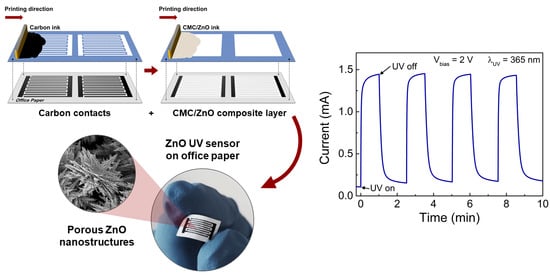
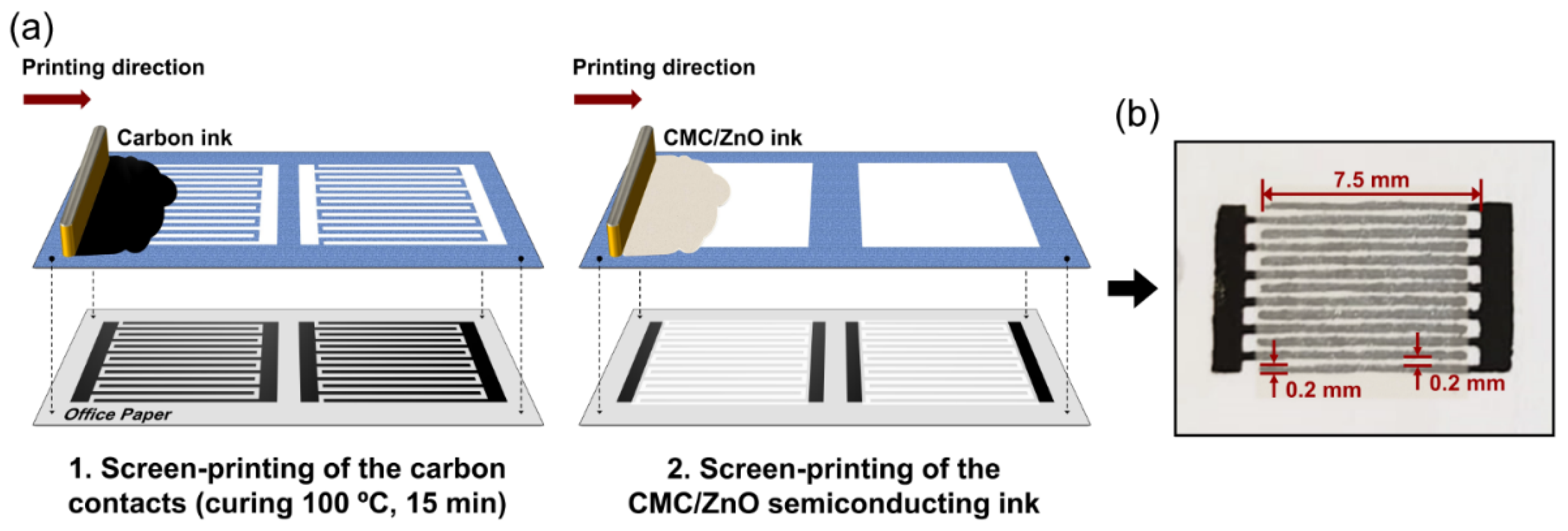
2.3. Fabrication and Characterization of the CMC/ZnO UV Sensors on Office Paper

As illustrated in Figure 1, carbon electrodes were screen-printed on office paper (80 g m−2, The Navigator Company, Portugal) using a conductive carbon paste (CRSN2644 C INK, Sun Chemical, USA), and a screen mold made of polyester with the following conditions: mesh model, 120–34; mesh count, 305 mesh/inch; aperture, 45 µm; thread diameter, 34 µm; opening, 30.5%; fabric thickness, 52–57 µm. The planar electrodes were screen-printed with an interdigital architecture composed of seven pairs of interdigital fingers with a width of 200 μm and length of 7.5 mm spaced from each other with a gap of 200 μm. The carbon electrodes were dried at 100 °C for 15 min in air.
The formulated CMC/ZnO ink was then screen-printed in a square shape (6 × 6 mm2) between the planar carbon electrodes with a different polyester screen (mesh model, 77–55; mesh count, 190 mesh/inch; aperture, 81 μm; thread diameter, 55 μm; opening, 30%; thickness, 88–97 μm) and dried at room temperature. Morphological characterization of the screen-printed CMC/ZnO layers was performed via SEM.

2.4. Electrical Characterization of the Screen-Printed UV Sensors on Office Paper

The sensor devices were electrically analyzed in air at room temperature using a microprobe station (Everbeing Int’l Corp., Taiwan) connected to a semiconductor parameter analyzer (Agilent 4155C, Keysight Technologies, Santa Rosa, CA, USA).
Chronoamperometry measurements were carried out with a constant applied bias voltage of 2 V. The screen-printed devices were irradiated with UV light at 365 nm using a fiber-coupled UV LED (4.1 mW, M365F1, Thorlabs Inc., Newton, NJ, USA) controlled by a DC4100 Controller from Thorlabs (Thorlabs Inc., New Jersey, USA) with a pulse train generator (Pulse Pal, Sanworks LLC, Rochester, NY, USA) programmed to turn on and off the UV LED at different intervals of time. The sensors were placed 2 cm from the light source and they were tested under a UV intensity of 8.66 mW cm−2. The sensors were exposed to 60 s of UV light followed by 90 s in the dark during several on/off cycles. The UV sensors were also tested under different applied bias voltages (0.25, 0.5, 1, and 2 V), and different UV light intensities (0.30, 0.91, 2.02, 4.27, and 8.66 mW cm−2). The UV light intensity was measured by a Suss MicroTec UV-Optometer (SÜSS MICROTEC SE, Garching, Germany).
To test the mechanical stability, a sensor was manually folded several times (100, 200, 500, and 1000 times) and flattened again before measuring its photoresponse to UV light under an applied voltage of 1 V and UV light intensity of 8.66 mW cm−2.

3. Results and Discussion

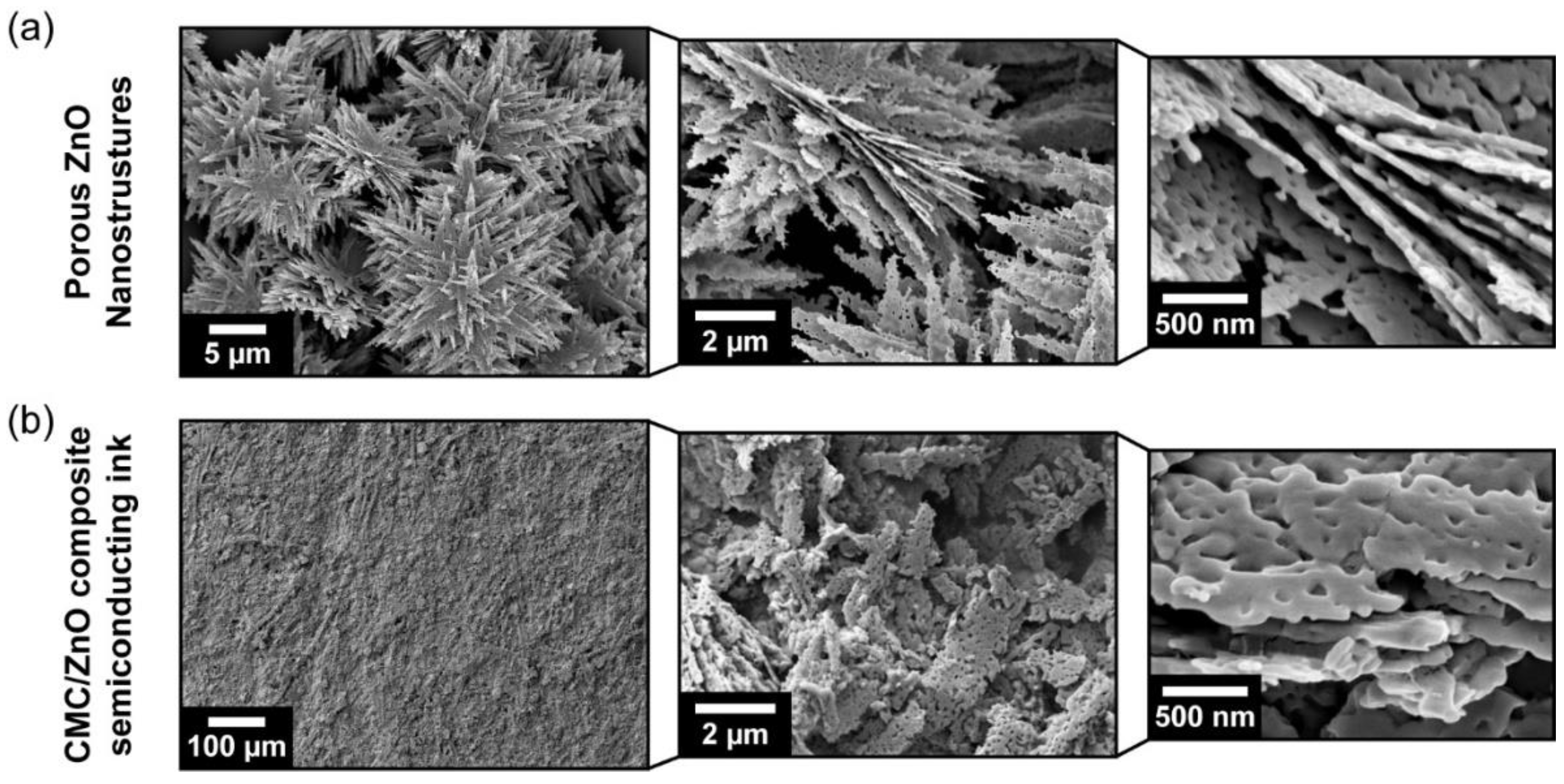
3.1. Characterization of Porous ZnO Nanostructures and CMC/ZnO Screen-Printed Films

As reported in our previous work [67], porous ZnO nanostructures were synthesized through a facile and fast hydrothermal method assisted by microwave irradiation, followed by a washing step to remove remnants of reagents from the synthesis and a calcination step in a furnace to thermally convert the resulting LZHC precursor into ZnO. As demonstrated in that work [67], a calcination process at 700 °C yields porous ZnO nanostructures with high crystallinity and larger pore size when compared to lower calcination temperatures, while ensuring a complete conversion of LZHC into ZnO. Therefore, this calcination temperature was selected to prepare the ZnO nanostructures in this work.
Figure 2a shows the SEM images of the produced ZnO powders for different magnifications. The porous ZnO nanostructures consist of many serrate-like porous nanoplates, which are tightly arranged into flower-like 3D hierarchical microstructures. The porous nanoplates are thin (<100 nm thickness), elongated (maximum length: <3.5 µm), and exhibit a highly porous surface with a pore size in the range of tens of nanometers which is formed during the calcination step.
On the other hand, the flower-like morphology is no longer visible on the screen-printed CMC/ZnO films (Figure 2b). The mechanical stress induced during the preparation of the inks and the screen-printing process promotes the disassembling of the 2D nanostructures, thus destroying their arrangement in the form of flowers. Despite all the challenges related to office paper surface roughness and absorption, a continuous CMC/ZnO composite film with good adhesion to the hydrogen-bonded cellulose fiber network is formed with a single screen-printing step at room temperature, showing no signs of cracks nor peeling. Higher magnifications of the screen-printed films reveal a dense and compact network of stacked and randomly oriented porous ZnO nanoplates. The elongated size of the porous ZnO nanostructures promotes a percolation network at low particle loading (10 wt%), thus reducing the amount of functional material needed to fabricate the semiconducting ink. Still, some micro-sized voids and agglomerates are visible, which contribute to their rough surface.

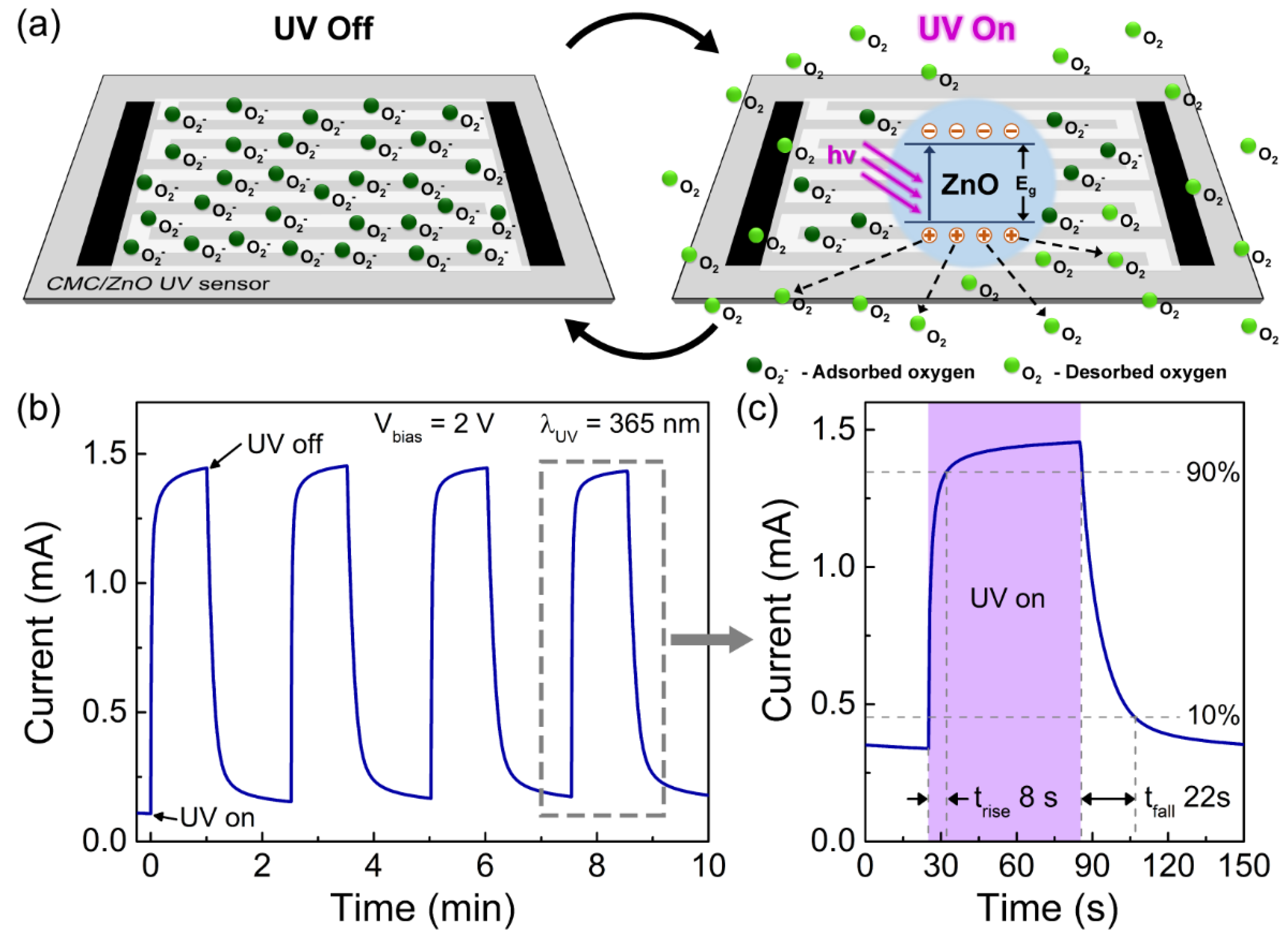
3.2. Characterization of Porous ZnO Nanostructures as UV Sensors

As depicted in Figure 3a, the UV sensing mechanism is based on the adsorption and desorption of oxygen-rich molecules on the surface of ZnO, and has been previously explained in several works [48,54,75,76]. In the dark, oxygen-rich molecules adsorb on the porous ZnO nanostructures due to the oxygen vacancies that exist in the ZnO surface, which are known to influence ZnO electrical conductivity [77]. By adsorbing on the surface of ZnO, the oxygen-rich molecules capture an electron from the conduction band, creating a depletion region on the nanostructures’ surface that results in an increase of the electrical resistance of the device. Electron-hole pairs are created when the ZnO layer is exposed to UV light with energy higher than the ZnO bandgap. The photogenerated holes migrate to the nanostructures’ surface, recombining with the previously captured electrons and, therefore, releasing the adsorbed oxygen molecules from the surface. The generated electrons from the absorption of UV light are now unpaired and available for conduction, leading to a decrease of the depletion region and a subsequent increase of the photocurrent in the UV sensor.
Figure 3b shows the photoelectrical response of the fabricated UV sensors over time for several UV on/off cycles under a bias voltage of 2 V. The photoresponse curve in this figure corresponds to the average response of three tested sensors. The tested sensors were exposed to UV light at 365 nm with a light intensity of 8.66 mW cm−2 for 60 s followed by 90 s in the dark. The sensors show a stable photoresponse after successive on/off UV cycles, reaching a maximum average photocurrent (Iph) of 1.45 ± 0.23 mA under UV light and an average dark current (Idark) of 0.11 ± 0.10 mA. This results in an average response current (ΔI = Iph−Idark) [78] around 1.34 ± 0.15 mA.
The responsivity (R) of the sensors can be determined by the following expression:
R = I p h I d a r k P U V
where PUV is the output power of the UV LED (3.1 mW for a UV light intensity of 8.66 mW cm−2 and an irradiated area of 36 mm2). The average responsivity of the tested sensors was found to be 432 ± 48 mA W−1. As displayed in Figure 3c, the switching response of the UV sensors was also determined to evaluate how fast they respond during (on-state) and after (off-state) exposure to UV light. Therefore, the rise time (trise) was determined by the time required to shift from 10 to 90% of the maximum photocurrent, while the fall time (tfall) corresponds to the time that it takes to decrease from 90 to 10% when the UV light is turned off [76,78,79]. These parameters were determined to be 8.2 ± 1.0 and 22.0 ± 2.3 s for trise and tfall, respectively.
The promising results obtained for the produced ZnO UV sensors can be attributed to the enhanced adsorption capacity for oxygen-rich molecules on the surface of the porous ZnO nanostructures due to their large specific surface area as well as the improvement of electron transport properties in ZnO as a result of both its high crystallinity [67] and plane contacts between the porous nanoplates [63]. Overall, the resistance of the sensing layer is strongly affected by the inter-nanostructure barrier at the contacts, meaning that the photoresponse of the sensor is mainly determined by the contacts between the ZnO nanostructures. In this case, the elongated nanoplate-shape of the porous ZnO nanostructures results not only in a more direct percolation path for electron transport due to the reduced nanoplates’ thickness (<100 nm) but also in plane-to-plane contacts between the particles. This means that the area of the contact plane is much larger when compared to other nanostructures’ morphologies (such as nanowires [80] for example) thus leading to enhanced sensing properties.
Table 1 shows a comparison between our results and the current state-of-the-art values in the field of UV sensors based either on ZnO nanostructures grown/deposited on paper substrates or ZnO/cellulose composites. Although these types of ZnO UV sensors have only been reported since the beginning of the last decade, most of the first published works do not provide a detailed characterization of the sensors. From Table 1, it is clear that the CMC/ZnO UV sensors fabricated in this work show the highest response current and responsivity. For instance, Figueira et al. [54] fabricated screen-printed ZnO UV sensors on cork substrates using an ethyl cellulose/ZnO commercial nanoparticles composite ink. Despite the similar methods involved in the fabrication process, these devices could only reach 20 µA under UV light, which is 100 times smaller than the response current obtained in this work. Besides, contrary to our work, a high loading content of small-sized (<100 nm) commercial ZnO nanoparticles (40 wt%) were needed to form a continuous and functional composite matrix on the irregular and punctually defective cork surface. Beyond the listed works displayed in Table 1, the screen-printed CMC/ZnO sensors on office paper also exhibit a comparable or even superior performance than some of recently published ZnO-based UV sensors comprising expensive materials and/or complex, time-consuming and energy-intensive processing methods [75,76,81,82,83,84,85].
Figure 4a,b depict the average photocurrent of the UV sensors under different applied voltages (0.25, 0.5, 1, and 2 V) and the corresponding response current (ΔI) and responsivity. The bias voltage plays an important role in the electron–hole pair separation, recombination, and transportation processes and, therefore, it determines the overall photoresponse of the UV sensor [78]. The response current of the sensor increased almost linearly from 0.14 ± 0.02 to 1.34 ± 0.15 mA when the applied voltage is varied from 0.25 to 2 V, respectively. Typically, ZnO nanostructures present high recombination rates, low carrier mobilities, and high resistivities [77,78], which means that applied voltages above 1 V are usually needed to obtain a good response to UV light [78]. In this work, the sensors presented a very good responsivity even for low applied voltages (<2 V), reaching a value of 43.9 ± 6.8 mA W−1 for 0.25 V. The low-voltage operation of the fabricated screen-printed sensors is compatible with the emerging concept of IoT and demonstrates that these devices can be powered by portable power supplies, such as thin-film batteries or solar cells [5,12,18,95]. To the best of our knowledge, this is the first report showing low-powered and low-cost ZnO-based UV sensors on paper substrates with a response current in the mA range, as previously evidenced by Table 1.
Figure 5a,b show the average photocurrent for different UV light intensities and the calculated response current and responsivity for an applied voltage of 1 V. In Figure 5b, the sensors’ response current increases with UV light intensity, shifting from 0.17 ± 0.02 mA for an intensity of 0.30 mW cm−2 to 0.52 ± 0.08 mA for an intensity of 8.66 mW cm−2. The UV light intensity is proportional to the number of photons irradiating the porous ZnO nanostructures for a certain UV wavelength. As such, when the UV intensity increases, the number of incident photons is higher and, consequently, more carriers are generated, and the response current is increased. On the other hand, the sensor’s responsivity decreases with increasing UV irradiance. This is expected since the response current remains in the same order of magnitude (10−1 mA) while the incident UV light power increases from 0.30 to 8.66 mW cm−2. As a result, the calculated responsivity (mA W−1) decreases with increasing UV light intensity. More importantly, the obtained results indicate that the produced UV sensors can respond to much weaker UV light, making these sensors suitable for the detection of low levels of UV light.
To evaluate the mechanical stability, a single CMC/ZnO UV sensor was manually folded successive times and then flattened again prior to being subjected to a UV light intensity of 8.66 mW cm−2 under an applied voltage of 1 V. The photoresponse was recorded after folding the sensor 100, 200, 500, and 1000 consecutive times. Figure 6a shows the normalized response current curves for the initial flat position and after being folded a different number of times. The response current reached by the sensor after 60 s of UV exposure decreased with the number of folds and its responsivity decreased by 1.5, 9, 20, and 21% after the sensor has been folded 100, 200, 500, and 1000 times, respectively, as depicted in Figure 6b. As illustrated by the inset in Figure 6b, when the ZnO sensor was folded in half, a folding crease appeared across the sensor’s layers and paper substrate, which was intensified as the number of folds increased. An SEM image of the crease folding area after the sensor had been folded 1000 times is shown in the left inset of Figure 6b. Here, some cracks are visible in the CMC/ZnO layer deposited on paper. These cracks and their length increased in both the electrodes and ZnO photoactive layer with the number of folds, consequently leading to a decrease in the UV sensor’s responsivity, since the path for the electrical carriers was broken in several places. Nonetheless, the produced ZnO sensors are capable of detecting UV light with very good responsivity even after being folded in half 1000 times, thus demonstrating their extremely high mechanical resistance. These results are of great significance since they validate the robustness of the fabricated ZnO UV sensors, therefore showing their potential to be used in wearable devices and smart packaging.

4. Conclusions

In summary, we demonstrated for the first time the use of porous ZnO nanostructures synthesized by microwave hydrothermal method to fabricate a water-based screen-printable ink where CMC was used as a binder. The CMC/ZnO composite ink was successfully screen-printed on office paper to be used as the photoactive layer in UV sensors.
The fabricated ZnO UV sensors showed promising results for application in low-power and flexible paper-based electronics. The tested sensors revealed a stable and good responsivity of 432 ± 48 mA W−1 with a response current of 1.34 ± 0.15 mA for an applied voltage of 2 V, which are the highest values reported in the literature for UV sensors based either on ZnO nanostructures grown/deposited on paper or ZnO/cellulose composites. Furthermore, the ZnO sensors showed good responsivities even under low UV light intensity (0.30 mW cm−2) and ultra-low applied voltage (0.25 V). The produced UV sensors were also tested after being folded up to 1000 consecutive times with a decrease of only 21% in the final responsivity value, hence proving their potential for wearable technologies and smart packaging.

Author Contributions

Conceptualization, S.H.F. and I.C.; methodology, S.H.F., I.C., J.V.P. and J.P.N.; investigation, S.H.F. and I.C.; software, S.H.F. and J.P.N.; resources, J.P.N., L.P., E.F. and R.M.; data curation, S.H.F.; writing—original draft preparation, S.H.F.; writing—review and editing, I.C., J.V.P., J.P.N., L.P., E.F. and R.M.; supervision, L.P., E.F. and R.M.; funding acquisition, L.P., E.F. and R.M. All authors have read and agreed to the published version of the manuscript.

Funding

This work is funded by National Funds through FCT—Portuguese Foundation for Science and Technology, reference UIDB/50025/2020-2023 and FCT/MCTES. This work also received funding from the European Community’s H2020 program under grant agreement No. 787410 (ERC-2018-AdG DIGISMART), No. 640598 (ERC-StG-2014, NEWFUN), and No. 952169 (SYNERGY, H2020-WIDESPREAD-2020-5, CSA). S.H.F. acknowledges the Portuguese Foundation for Science and Technology for the AdvaMTech PhD program scholarship PD/BD/114086/2015 and IDS-FunMat-INNO project FPA2016/EIT/EIT RawMaterials Grant Agreement 17184. I.C. acknowledges the Portuguese Foundation for Science and Technology for the PhD scholarship SFRH/BD/126409/2016.

Institutional Review Board Statement

Not applicable.

Informed Consent Statement

Not applicable.

Data Availability Statement

The data presented in this study are available on request from the corresponding author.

Conflicts of Interest

The authors declare no conflict of interest.

References

  1. Nandy, S.; Goswami, S.; Marques, A.; Gaspar, D.; Grey, P.; Cunha, I.; Nunes, D.; Pimentel, A.; Igreja, R.; Barquinha, P.; et al. Cellulose: A Contribution for the Zero e-Waste Challenge. Adv. Mater. Technol. 2021, 2000994. [Google Scholar] [CrossRef]
  2. Zschieschang, U.; Klauk, H. Organic transistors on paper: A brief review. J. Mater. Chem. C 2019, 7, 5522–5533. [Google Scholar] [CrossRef] [Green Version]
  3. Ha, D.; Fang, Z.; Zhitenev, N.B. Paper in Electronic and Optoelectronic Devices. Adv. Electron. Mater. 2018, 4, 1700593. [Google Scholar] [CrossRef]
  4. Zhang, Y.; Zhang, L.; Cui, K.; Ge, S.; Cheng, X.; Yan, M.; Yu, J.; Liu, H. Flexible electronics based on micro/nanostructured paper. Adv. Mater. 2018, 30, 1–39. [Google Scholar] [CrossRef] [Green Version]
  5. Martins, R.; Gaspar, D.; Mendes, M.J.; Pereira, L.; Martins, J.; Bahubalindruni, P.; Barquinha, P.; Fortunato, E. Papertronics: Multigate paper transistor for multifunction applications. Appl. Mater. Today 2018, 12, 402–414. [Google Scholar] [CrossRef]
  6. Russo, A.; Ahn, B.Y.; Adams, J.J.; Duoss, E.B.; Bernhard, J.T.; Lewis, J.A. Pen-on-Paper Flexible Electronics. Adv. Mater. 2011, 23, 3426–3430. [Google Scholar] [CrossRef]
  7. Kurra, N.; Kulkarni, G.U. Pencil-on-paper: Electronic devices. Lab Chip 2013, 13, 2866. [Google Scholar] [CrossRef] [PubMed]
  8. Lien, D.-H.; Kao, Z.-K.; Huang, T.-H.; Liao, Y.-C.; Lee, S.-C.; He, J.-H. All-Printed Paper Memory. ACS Nano 2014, 8, 7613–7619. [Google Scholar] [CrossRef] [PubMed]
  9. Sia, S. Cutting edge: Thin, lightweight, foldable thermochromic displays on paper. Lab Chip 2009, 9, 2763. [Google Scholar] [CrossRef]
  10. Tehrani, P.; Hennerdal, L.-O.; Dyer, A.L.; Reynolds, J.R.; Berggren, M. Improving the contrast of all-printed electrochromic polymer on paper displays. J. Mater. Chem. 2009, 19, 1799. [Google Scholar] [CrossRef]
  11. Yoon, B.; Ham, D.-Y.; Yarimaga, O.; An, H.; Lee, C.W.; Kim, J.-M. Inkjet Printing of Conjugated Polymer Precursors on Paper Substrates for Colorimetric Sensing and Flexible Electrothermochromic Display. Adv. Mater. 2011, 23, 5492–5497. [Google Scholar] [CrossRef] [PubMed]
  12. Vicente, T.A.; Araújo, A.; Mendes, M.J.; Nunes, D.; Oliveira, M.J.; Sanchez-Sobrado, O.; Ferreira, M.P.; Águas, H.; Fortunato, E.; Martins, R. Multifunctional cellulose-paper for light harvesting and smart sensing applications. J. Mater. Chem. C 2018, 6, 3143–3181. [Google Scholar] [CrossRef]
  13. Nuchtavorn, N.; Macka, M. A novel highly flexible, simple, rapid and low-cost fabrication tool for paper-based microfluidic devices (μPADs) using technical drawing pens and in-house formulated aqueous inks. Anal. Chim. Acta 2016, 919, 70–77. [Google Scholar] [CrossRef] [PubMed]
  14. Hyun, W.J.; Secor, E.B.; Rojas, G.A.; Hersam, M.C.; Francis, L.F.; Frisbie, C.D. All-Printed, Foldable Organic Thin-Film Transistors on Glassine Paper. Adv. Mater. 2015, 27, 7058–7064. [Google Scholar] [CrossRef]
  15. Thiemann, S.; Sachnov, S.J.; Pettersson, F.; Bollström, R.; Österbacka, R.; Wasserscheid, P.; Zaumseil, J. Cellulose-Based Ionogels for Paper Electronics. Adv. Funct. Mater. 2014, 24, 625–634. [Google Scholar] [CrossRef]
  16. Ihalainen, P.; Määttänen, A.; Järnström, J.; Tobjörk, D.; Österbacka, R.; Peltonen, J. Influence of Surface Properties of Coated Papers on Printed Electronics. Ind. Eng. Chem. Res. 2012, 51, 6025–6036. [Google Scholar] [CrossRef]
  17. Grau, G.; Kitsomboonloha, R.; Swisher, S.L.; Kang, H.; Subramanian, V. Printed Transistors on Paper: Towards Smart Consumer Product Packaging. Adv. Funct. Mater. 2014, 24, 5067–5074. [Google Scholar] [CrossRef]
  18. Hong, K.; Kim, S.H.; Lee, K.H.; Frisbie, C.D. Printed, sub-2V ZnO Electrolyte Gated Transistors and Inverters on Plastic. Adv. Mater. 2013, 25, 3413–3418. [Google Scholar] [CrossRef]
  19. Zheng, Y.; He, Z.; Gao, Y.; Liu, J. Direct Desktop Printed-Circuits-on-Paper Flexible Electronics. Sci. Rep. 2013, 3, 1786. [Google Scholar] [CrossRef]
  20. Carvalho, J.T.; Dubceac, V.; Grey, P.; Cunha, I.; Fortunato, E.; Martins, R.; Clausner, A.; Zschech, E.; Pereira, L. Fully printed zinc oxide electrolyte-gated transistors on paper. Nanomaterials 2019, 9, 169. [Google Scholar] [CrossRef] [Green Version]
  21. Grey, P.; Gaspar, D.; Cunha, I.; Barras, R.; Carvalho, J.T.; Ribas, J.R.; Fortunato, E.; Martins, R.; Pereira, L. Handwritten Oxide Electronics on Paper. Adv. Mater. Technol. 2017, 2, 170009. [Google Scholar] [CrossRef]
  22. Fortunato, E.; Correia, N.; Barquinha, P.; Pereira, L.; Goncalves, G.; Martins, R. High-Performance Flexible Hybrid Field-Effect Transistors Based on Cellulose Fiber Paper. IEEE Electron Device Lett. 2008, 29, 988–990. [Google Scholar] [CrossRef] [Green Version]
  23. Hu, G.; Kang, J.; Ng, L.W.T.; Zhu, X.; Howe, R.C.T.; Jones, C.G.; Hersam, M.C.; Hasan, T. Functional inks and printing of two-dimensional materials. Chem. Soc. Rev. 2018, 47, 3265–3300. [Google Scholar] [CrossRef] [Green Version]
  24. Kamyshny, A.; Magdassi, S. Conductive Nanomaterials for Printed Electronics. Small 2014, 10, 3515–3535. [Google Scholar] [CrossRef]
  25. Wu, W. Inorganic nanomaterials for printed electronics: A review. Nanoscale 2017, 9, 7342–7372. [Google Scholar] [CrossRef] [PubMed]
  26. Capanema, N.S.V.; Mansur, A.A.P.; Carvalho, S.M.; Mansur, L.L.; Ramos, C.P.; Lage, A.P.; Mansur, H.S. Physicochemical properties and antimicrobial activity of biocompatible carboxymethylcellulose-silver nanoparticle hybrids for wound dressing and epidermal repair. J. Appl. Polym. Sci. 2018, 135, 45812. [Google Scholar] [CrossRef]
  27. Solomon, M.M.; Gerengi, H.; Umoren, S.A. Carboxymethyl Cellulose/Silver Nanoparticles Composite: Synthesis, Characterization and Application as a Benign Corrosion Inhibitor for St37 Steel in 15% H2SO4 Medium. ACS Appl. Mater. Interfaces 2017, 9, 6376–6389. [Google Scholar] [CrossRef]
  28. Kamal, T.; Ahmad, I.; Khan, S.B.; Ul-Islam, M.; Asiri, A.M. Microwave Assisted Synthesis and Carboxymethyl Cellulose Stabilized Copper Nanoparticles on Bacterial Cellulose Nanofibers Support for Pollutants Degradation. J. Polym. Environ. 2019, 27, 2867–2877. [Google Scholar] [CrossRef]
  29. Bollström, R.; Tobjörk, D.; Dolietis, P.; Salminen, P.; Preston, J.; Österbacka, R.; Toivakka, M. Printability of functional inks on multilayer curtain coated paper. Chem. Eng. Process. Process Intensif. 2013, 68, 13–20. [Google Scholar] [CrossRef]
  30. Tobjörk, D.; Österbacka, R. Paper electronics. Adv. Mater. 2011, 23, 1935–1961. [Google Scholar] [CrossRef]
  31. Agate, S.; Joyce, M.; Lucia, L.; Pal, L. Cellulose and nanocellulose-based flexible-hybrid printed electronics and conductive composites—A review. Carbohydr. Polym. 2018, 198, 249–260. [Google Scholar] [CrossRef]
  32. Inukai, K.; Takahashi, Y.; Ri, K.; Shin, W. Rheological analysis of ceramic pastes with ethyl cellulose for screen-printing. Ceram. Int. 2015, 41, 5959–5966. [Google Scholar] [CrossRef]
  33. Faddoul, R.; Reverdy-Bruas, N.; Blayo, A. Formulation and screen printing of water based conductive flake silver pastes onto green ceramic tapes for electronic applications. Mater. Sci. Eng. B 2012, 177, 1053–1066. [Google Scholar] [CrossRef]
  34. Lin, H.W.; Chang, C.P.; Hwu, W.H.; Ger, M.D. The rheological behaviors of screen-printing pastes. J. Mater. Process. Technol. 2008, 197, 284–291. [Google Scholar] [CrossRef]
  35. Wang, Z.L. Zinc oxide nanostructures: Growth, properties and applications. J. Phys. Condens. Matter 2004, 16, R829–R858. [Google Scholar] [CrossRef]
  36. Nunes, D.; Pimentel, A.; Goncalves, A.; Pereira, S.; Branquinho, R.; Barquinha, P.; Fortunato, E.; Martins, R. Metal oxide nanostructures for sensor applications. Semicond. Sci. Technol. 2019, 34, 043001. [Google Scholar] [CrossRef] [Green Version]
  37. Arrabito, G.; Aleeva, Y.; Pezzilli, R.; Ferrara, V.; Medaglia, P.G.; Pignataro, B.; Prestopino, G. Printing ZnO Inks: From Principles to Devices. Crystals 2020, 10, 449. [Google Scholar] [CrossRef]
  38. Agarwal, H.; Venkat Kumar, S.; Rajeshkumar, S. A review on green synthesis of zinc oxide nanoparticles—An eco-friendly approach. Resour. Technol. 2017, 3, 406–413. [Google Scholar] [CrossRef]
  39. Naveed Ul Haq, A.; Nadhman, A.; Ullah, I.; Mustafa, G.; Yasinzai, M.; Khan, I. Synthesis Approaches of Zinc Oxide Nanoparticles: The Dilemma of Ecotoxicity. J. Nanomater. 2017, 2017, 8510342. [Google Scholar] [CrossRef]
  40. Laurenti, M.; Cauda, V. Porous zinc oxide thin films: Synthesis approaches and applications. Coatings 2018, 8, 67. [Google Scholar] [CrossRef] [Green Version]
  41. Mishra, Y.K.; Adelung, R. ZnO tetrapod materials for functional applications. Mater. Today 2018, 21, 631–651. [Google Scholar] [CrossRef]
  42. Kołodziejczak-Radzimska, A.; Jesionowski, T. Zinc Oxide—From Synthesis to Application: A Review. Materials 2014, 7, 2833–2881. [Google Scholar] [CrossRef] [Green Version]
  43. Fortunato, E.; Nunes, P.; Marques, A.; Costa, D.; Aguas, H.; Ferreira, I.; Godinho, M.H.; Almeida, P.L.; Borges, J.P.; Martins, R. Transparent, conductive ZnO:Al thin film deposited on polymer substrates by RF magnetron sputtering. Surf. Coatings Technol. 2002, 152, 247–251. [Google Scholar] [CrossRef]
  44. Pimentel, A.; Gonçalves, A.; Marques, A.; Martins, R.; Fortunato, E. Role of the thickness on the electrical and optical performances of undoped polycrystalline zinc oxide films used as UV detectors. J. Non-Cryst. Solids 2006, 352, 1448–1452. [Google Scholar] [CrossRef]
  45. Nunes, P.; Fortunato, E.; Lopes, A.; Martins, R. Influence of the deposition conditions on the gas sensitivity of zinc oxide thin films deposited by spray pyrolysis. Int. J. Inorg. Mater. 2001, 3, 1129–1131. [Google Scholar] [CrossRef]
  46. Collins, M.J. Introduction to Microwave Chemistry. In Microwave Synthesis: Chemistry at the Speed of Light; Hayes, B.L., Ed.; CEM Publishing: Matthews, NC, USA, 2002; pp. 11–27. ISBN 0-9722229-01. [Google Scholar]
  47. Mirzaei, A.; Neri, G. Microwave-assisted synthesis of metal oxide nanostructures for gas sensing application: A review. Sens. Actuators B Chem. 2016, 237, 749–775. [Google Scholar] [CrossRef]
  48. Ferreira, S.H.; Deuermeier, J.; Sequeira, S.; Nunes, D.; Gonçalves, A.M.F.; Martins, R.; Monteiro, R.C.C.; Fortunato, E. Industrial waste residue converted into value-added ZnO for optoelectronic applications. ACS Appl. Electron. Mater. 2020, 2, 1960–1969. [Google Scholar] [CrossRef]
  49. Pimentel, A.; Samouco, A.; Nunes, D.; Araújo, A.; Martins, R.; Fortunato, E. Ultra-fast microwave synthesis of ZnO nanorods on cellulose substrates for UV sensor applications. Materials 2017, 10, 1308. [Google Scholar] [CrossRef] [Green Version]
  50. Matias, M.L.; Nunes, D.; Pimentel, A.; Ferreira, S.H.; Borda d’Agua, R.; Duarte, M.P.; Fortunato, E.; Martins, R. Paper-Based Nanoplatforms for Multifunctional Applications. J. Nanomater. 2019, 2019, 6501923. [Google Scholar] [CrossRef] [Green Version]
  51. Filip, A.; Musat, V.; Tigau, N.; Polosan, S.; Pimentel, A.; Ferreira, S.; Gomes, D.; Calmeiro, T.; Martins, R.; Fortunato, E. ZnO nanostructures grown on ITO coated glass substrate by hybrid microwave-assisted hydrothermal method. Optik 2020, 208, 164372. [Google Scholar] [CrossRef]
  52. Wojnarowicz, J.; Chudoba, T.; Lojkowski, W. A Review of Microwave Synthesis of Zinc Oxide Nanomaterials: Reactants, Process Parameters and Morphologies. Nanomaterials 2020, 10, 1086. [Google Scholar] [CrossRef]
  53. Claro, P.I.C.; Marques, A.C.; Cunha, I.; Martins, R.F.P.; Pereira, L.M.N.; Marconcini, J.M.; Mattoso, L.H.C.; Fortunato, E. Tuning the Electrical Properties of Cellulose Nanocrystals through Laser-Induced Graphitization for UV Photodetectors. ACS Appl. Nano Mater. 2021. [Google Scholar] [CrossRef]
  54. Figueira, J.; Gaspar, C.; Carvalho, J.T.; Loureiro, J.; Fortunato, E.; Martins, R.; Pereira, L. Sustainable Fully Printed UV Sensors on Cork Using Zinc Oxide/Ethylcellulose Inks. Micromachines 2019, 10, 601. [Google Scholar] [CrossRef] [Green Version]
  55. Zargar, R.A.; Chackrabarti, S.; Joseph, S.; Khan, M.S.; Husain, R.; Hafiz, A.K. Synthesis and characterization of screen printed ZnO films for solar cell applications. Optik 2015, 126, 4171–4174. [Google Scholar] [CrossRef]
  56. Fekete, M.; Riedel, W.; Patti, A.F.; Spiccia, L. Photoelectrochemical water oxidation by screen printed ZnO nanoparticle films: Effect of pH on catalytic activity and stability. Nanoscale 2014, 6, 7585–7593. [Google Scholar] [CrossRef]
  57. Manjunath, G.; Pujari, S.; Patil, D.R.; Mandal, S. A scalable screen-printed high performance ZnO-UV and Gas Sensor: Effect of solution combustion. Mater. Sci. Semicond. Process. 2020, 107, 104828. [Google Scholar] [CrossRef]
  58. Wen, M.J.; Subramani, S.; Devarajan, M.; Sulaiman, F. Effect of ethyl cellulose on thermal resistivity of thixotropic ZnO nano-particle paste for thermal interface material in light emitting diode application. Mater. Sci. Semicond. Process. 2017, 58, 61–67. [Google Scholar] [CrossRef]
  59. Jang, J.S.; Lee, S.E.; Choi, S.J.; Koo, W.T.; Kim, D.H.; Shin, H.; Park, H.J.; Kim, I.D. Heterogeneous, Porous 2D Oxide Sheets via Rapid Galvanic Replacement: Toward Superior HCHO Sensing Application. Adv. Funct. Mater. 2019, 29, 1–10. [Google Scholar] [CrossRef]
  60. Xie, X.; Wang, X.; Tian, J.; Song, X.; Wei, N.; Cui, H. Growth of porous ZnO single crystal hierarchical architectures with ultrahigh sensing performances to ethanol and acetone gases. Ceram. Int. 2017, 43, 1121–1128. [Google Scholar] [CrossRef]
  61. Li, B.; Wang, Y. Hierarchically assembled porous ZnO microstructures and applications in a gas sensor. Superlattices Microstruct. 2011, 49, 433–440. [Google Scholar] [CrossRef]
  62. Chen, M.; Wang, Z.; Han, D.; Gu, F.; Guo, G. Porous ZnO polygonal nanoflakes: Synthesis, use in high-sensitivity NO 2 gas sensor, and proposed mechanism of gas sensing. J. Phys. Chem. C 2011, 115, 12763–12773. [Google Scholar] [CrossRef]
  63. Zhang, L.; Zhao, J.; Lu, H.; Li, L.; Zheng, J.; Li, H.; Zhu, Z. Facile synthesis and ultrahigh ethanol response of hierarchically porous ZnO nanosheets. Sens. Actuators B Chem. 2012, 161, 209–215. [Google Scholar] [CrossRef]
  64. Chang, J.; Ahmad, M.Z.; Wlodarski, W.; Waclawik, E.R. Self-assembled 3D ZnO porous structures with exposed reactive {0001} facets and their enhanced gas sensitivity. Sensors 2013, 13, 8445–8460. [Google Scholar] [CrossRef]
  65. Qiu, Y.; Chen, W.; Yang, S. Facile hydrothermal preparation of hierarchically assembled, porous single-crystalline ZnO nanoplates and their application in dye-sensitized solar cells. J. Mater. Chem. 2010, 20, 1001–1006. [Google Scholar] [CrossRef]
  66. Teng, Y.; Mo, M.; Li, Y.; Xue, J.; Zhao, H. Amorphous carbon-coated ZnO porous nanosheets: Facile fabrication and application in lithium- and sodium-ion batteries. J. Alloys Compd. 2018, 744, 712–720. [Google Scholar] [CrossRef]
  67. Ferreira, S.H.; Morais, M.; Nunes, D.; Oliveira, M.J.; Rovisco, A.; Pimentel, A.; Águas, H.; Fortunato, E.; Martins, R. High UV and Sunlight Photocatalytic Performance of Porous ZnO Nanostructures Synthesized by a Facile and Fast Microwave Hydrothermal Method. Materials 2021, 14, 2385. [Google Scholar] [CrossRef] [PubMed]
  68. Liu, S.; Li, C.; Yu, J.; Xiang, Q. Improved visible-light photocatalytic activity of porous carbon self-doped ZnO nanosheet-assembled flowers. CrystEngComm 2011, 13, 2533–2541. [Google Scholar] [CrossRef]
  69. Liu, D.; Lv, Y.; Zhang, M.; Liu, Y.; Zhu, Y.; Zong, R.; Zhu, Y. Defect-related photoluminescence and photocatalytic properties of porous ZnO nanosheets. J. Mater. Chem. A 2014, 2, 15377–15388. [Google Scholar] [CrossRef]
  70. Yang, H.; Ni, S.Q.; Jiang, X.; Jiang, W.; Zhan, J. In situ fabrication of single-crystalline porous ZnO nanoplates on zinc foil to support silver nanoparticles as a stable SERS substrate. CrystEngComm 2012, 14, 6023–6028. [Google Scholar] [CrossRef]
  71. Bitenc, M.; Marinšek, M.; Crnjak Orel, Z. Preparation and characterization of zinc hydroxide carbonate and porous zinc oxide particles. J. Eur. Ceram. Soc. 2008, 28, 2915–2921. [Google Scholar] [CrossRef]
  72. Gu, F.; You, D.; Wang, Z.; Han, D.; Guo, G. Improvement of gas-sensing property by defect engineering in microwave-assisted synthesized 3D ZnO nanostructures. Sens. Actuators B Chem. 2014, 204, 342–350. [Google Scholar] [CrossRef]
  73. Zhang, Y.; Liu, C.; Gong, F.; Jiu, B.; Li, F. Large scale synthesis of hexagonal simonkolleit nanosheets for ZnO gas sensors with enhanced performances. Mater. Lett. 2017, 186, 7–11. [Google Scholar] [CrossRef]
  74. Ferreira, S.H.; Rovisco, A.; dos Santos, A.; Águas, H.; Igreja, R.; Barquinha, P.; Fortunato, E.; Martins, R. Porous ZnO Nanostructures Synthesized by Microwave Hydrothermal Method for Energy Harvesting Applications. In Nanopores; Ameen, S., Ed.; IntechOpen: London, UK, 2021; ISBN 978-1-83880-210-3. [Google Scholar]
  75. Tran, V.T.; Wei, Y.; Yang, H.; Zhan, Z.; Du, H. All-inkjet-printed flexible ZnO micro photodetector for a wearable UV monitoring device. Nanotechnology 2017, 28, 095204. [Google Scholar] [CrossRef] [PubMed]
  76. Xu, Q.; Cheng, L.; Meng, L.; Wang, Z.; Bai, S.; Tian, X.; Jia, X.; Qin, Y. Flexible Self-Powered ZnO Film UV Sensor with a High Response. ACS Appl. Mater. Interfaces 2019, 11, 26127–26133. [Google Scholar] [CrossRef] [PubMed]
  77. Garlapati, S.K.; Divya, M.; Breitung, B.; Kruk, R.; Hahn, H.; Dasgupta, S. Printed Electronics Based on Inorganic Semiconductors: From Processes and Materials to Devices. Adv. Mater. 2018, 30, 1–55. [Google Scholar] [CrossRef]
  78. Deka Boruah, B. Zinc oxide ultraviolet photodetectors: Rapid progress from conventional to self-powered photodetectors. Nanoscale Adv. 2019, 1, 2059–2085. [Google Scholar] [CrossRef] [Green Version]
  79. Li, Y.; Della Valle, F.; Simonnet, M.; Yamada, I.; Delaunay, J.J. High-performance UV detector made of ultra-long ZnO bridging nanowires. Nanotechnology 2009, 20, 045501. [Google Scholar] [CrossRef] [PubMed]
  80. Sysoev, V.V.; Goschnick, J.; Schneider, T.; Strelcov, E.; Kolmakov, A. A gradient microarray electronic nose based on percolating SnO 2 nanowire sensing elements. Nano Lett. 2007, 7, 3182–3188. [Google Scholar] [CrossRef] [PubMed]
  81. Humayun, Q.; Kashif, M.; Hashim, U.; Qurashi, A. Selective growth of ZnO nanorods on microgap electrodes and their applications in UV sensors. Nanoscale Res. Lett. 2014, 9, 29. [Google Scholar] [CrossRef] [PubMed] [Green Version]
  82. Lee, D.; Seol, M.-L.; Motilal, G.; Kim, B.; Moon, D.-I.; Han, J.-W.; Meyyappan, M. All 3D-Printed Flexible ZnO UV Photodetector on an Ultraflat Substrate. ACS Sens. 2020, 5, 1028–1032. [Google Scholar] [CrossRef] [PubMed]
  83. Asib, N.A.M.; Husairi, F.S.; Eswar, K.A.; Afaah, A.N.; Mamat, M.H.; Rusop, M.; Khusaimi, Z. Developing high-sensitivity UV sensors based on ZnO nanorods grown on TiO2 seed layer films using solution immersion method. Sens. Actuators A Phys. 2020, 302, 111827. [Google Scholar] [CrossRef]
  84. Gedamu, D.; Paulowicz, I.; Kaps, S.; Lupan, O.; Wille, S.; Haidarschin, G.; Mishra, Y.K.; Adelung, R. Rapid fabrication technique for interpenetrated ZnO nanotetrapod networks for fast UV sensors. Adv. Mater. 2014, 26, 1541–1550. [Google Scholar] [CrossRef]
  85. Bai, S.; Wu, W.; Qin, Y.; Cui, N.; Bayerl, D.J.; Wang, X. High-performance integrated ZnO nanowire UV sensors on rigid and flexible substrates. Adv. Funct. Mater. 2011, 21, 4464–4469. [Google Scholar] [CrossRef]
  86. Manekkathodi, A.; Lu, M.Y.; Wang, C.W.; Chen, L.J. Direct growth of aligned zinc oxide nanorods on paper substrates for low-cost flexible electronics. Adv. Mater. 2010, 22, 4059–4063. [Google Scholar] [CrossRef] [PubMed]
  87. Gimenez, A.J.; Yáñez-Limón, J.M.; Seminario, J.M. ZnO-paper based photoconductive UV sensor. J. Phys. Chem. C 2011, 115, 282–287. [Google Scholar] [CrossRef]
  88. Ul Hasan, K.; Nur, O.; Willander, M. Screen printed ZnO ultraviolet photoconductive sensor on pencil drawn circuitry over paper. Appl. Phys. Lett. 2012, 100, 21104. [Google Scholar] [CrossRef] [Green Version]
  89. Kiasari, N.M.; Soltanian, S.; Gholamkhass, B.; Servati, P. Sketching functional, ubiquitous ZnO nano-sensors on paper. RSC Adv. 2014, 4, 19663–19667. [Google Scholar] [CrossRef]
  90. Sahoo, K.; Biswas, A.; Nayak, J. Effect of synthesis temperature on the UV sensing properties of ZnO-cellulose nanocomposite powder. Sens. Actuators A Phys. 2017, 267, 99–105. [Google Scholar] [CrossRef]
  91. Veerla, R.S.; Sahatiya, P.; Badhulika, S. Fabrication of a flexible UV photodetector and disposable photoresponsive uric acid sensor by direct writing of ZnO pencil on paper. J. Mater. Chem. C 2017, 5, 10231–10240. [Google Scholar] [CrossRef]
  92. Mun, S.; Kim, H.C.; Ko, H.U.; Zhai, L.; Kim, J.W.; Kim, J. Flexible cellulose and ZnO hybrid nanocomposite and its UV sensing characteristics. Sci. Technol. Adv. Mater. 2017, 18, 437–446. [Google Scholar] [CrossRef] [PubMed] [Green Version]
  93. Sahoo, K.; Mohanty, B.; Biswas, A.; Nayak, J. Role of hexamethylenetetramine in ZnO-cellulose nanocomposite enabled UV and humidity sensor. Mater. Sci. Semicond. Process. 2020, 105, 104699. [Google Scholar] [CrossRef]
  94. Dubourg, G.; Radovic, M.; Vasic, B. Laser-tunable printed zno nanoparticles for paper-based uv sensors with reduced humidity interference. Nanomaterials 2021, 11, 80. [Google Scholar] [CrossRef] [PubMed]
  95. Adila, A.S.; Husam, A.; Husi, G. Towards the self-powered Internet of Things (IoT) by energy harvesting: Trends and technologies for green IoT. In Proceedings of the 2018 2nd International Symposium on Small-Scale Intelligent Manufacturing Systems (SIMS), Cavan, Ireland, 16–18 April 2018; IEEE: Piscataway, NJ, USA, 2018; pp. 1–5, ISBN 978-1-5386-4437-9. [Google Scholar]
Figure 1. (a) Schematic of the fabrication process of the screen-printed CMC/ZnO UV sensor on office paper. (b) Optical image of a single screen-printed UV sensor on office paper.
Chemosensors 09 00192 g001
Figure 2. SEM images of (a) the porous ZnO structures assembled into 3D flower-like hierarchical structures obtained by hydrothermal method assisted by microwave irradiation, and (b) the screen-printed CMC/porous ZnO nanostructures composite ink on office paper.
Chemosensors 09 00192 g002
Figure 3. (a) Schematic of the UV sensing mechanism of the screen-printed CMC/ZnO UV sensor on office paper. (b) Average photoresponse of the UV sensor during several on/off UV cycles under a bias voltage of 2 V for a UV wavelength of 365 nm and an intensity of 8.66 mW cm−2. (c) Magnification of one on/off UV cycle indicating the respective rise (trise) and fall (tfall) times.
Chemosensors 09 00192 g003
Figure 4. (a) Average photoresponse of the screen-printed CMC/ZnO UV sensor on office paper under different bias voltages for a UV light intensity of 8.66 mW cm−2. (b) Response current and respective responsivity for different applied voltages.
Chemosensors 09 00192 g004
Figure 5. (a) Average photoresponse of the screen-printed CMC/ZnO UV sensor on office paper for different UV light intensities under a bias voltage of 1 V. (b) Response current and respective responsivity for different UV light intensities.
Chemosensors 09 00192 g005
Figure 6. (a) Comparison of the normalized response current of a single screen-printed ZnO UV sensor in a flat position before and after being folded up to 1000 successive times. (b) Normalized responsivity of the UV sensor as a function of the number of folds. Inset of an illustration of the folding process and an SEM image showing the resulting cracks in the folding crease line of the sensor after being folded 1000 consecutive times.
Chemosensors 09 00192 g006
Table 1. Comparison of typical measurement parameters (Vbias and UV light intensity) and respective UV sensor characteristics (trise, tfall, ΔI, and R) obtained for devices based either on ZnO nanostructures grown/deposited on paper substrates or ZnO/cellulose composites.
MaterialsUV Intensity (mW cm−2)Vbias
(V)
trise
(s)
tfall
(s)
ΔI
(mA)
R
(mA W−1)
Reference
CMC/ZnO composite on office paper8.662.08.2 ± 1.022.0 ± 2.31.34 ± 0.15432 ± 48This work
ZnO nanorods on paperN/A5.0N/AN/A5.50 × 10−3N/AManekkathodi et al. 2010 [86]
ZnO powder on paperN/A10.0N/AN/A7.00 × 10−3N/AGimenez et al.
2011 [87]
ZnO nanocrystals on paperN/A1.0N/AN/A9.00 × 10−4N/AHasan et al.
2012 [88]
ZnO nanoparticles on paper1.22N/A6.03.0N/AN/AKiasari et al.
2014 [89]
ZnO–cellulose nanocomposite pelletsN/A5.015.010.07.76 × 10−3N/ASahoo et al.
2017 [90]
Direct writing of ZnO nanoparticles on paper3.101.033.1918.132.20 × 10−4N/AVeerla et al.
2017 [91]
Commercial ZnO nanoparticles on paperN/A5.014.77.5N/AN/AGrey et al.
2017 [21]
ZnO nanorods grown on Whatman paperN/A10.057.065.09.60 × 10−31.19 × 10⁻³Pimentel et al.
2017 [49]
ZnO nanorods grown on cellulose film2.60N/A<1N/A1.34 × 10−3N/AMun et al.
2017 [92]
ZnO nanorods grown on Whatman paperN/A10.0N/A109.04.90 × 10−30.61 × 10⁻³Matias et al.
2019 [50]
ZnO/ethylcellulose composite on corkN/A5.03.61.52.00 × 10−2N/AFigueira et al.
2019 [54]
ZnO–cellulose nanocomposite pellets60.005.08.010.03.09 × 10−2N/ASahoo et al.
2020 [93]
Commercial ZnO nanoparticles on paper105.010.010.0N/AN/ADubourg et al. 2021 [94]
Publisher’s Note: MDPI stays neutral with regard to jurisdictional claims in published maps and institutional affiliations.

