
Driving Circuit Design for Piezo Ceramics Considering Transformer Leakage Inductance


Department of Electrical Engineering, National University of Tainan, Tainan 700301, Taiwan
*
Author to whom correspondence should be addressed.
Processes 2023, 11(1), 247; https://0-doi-org.brum.beds.ac.uk/10.3390/pr11010247
Submission received: 6 December 2022
/
Revised: 6 January 2023
/
Accepted: 7 January 2023
/
Published: 12 January 2023
(This article belongs to the Section Process Control and Monitoring)
Abstract
:This paper presents the circuit and control method for piezo-ceramic drives. With the proposed method, a gap is imposed in the transformer core to increase the leakage inductance. This flattens the voltage gain curve of the piezo-ceramic driver over the resonant frequency range, so voltage gain changes are insensitive to frequency changes. In addition, resonant frequency tracking and power control methods are developed, while the circuit is capable of zero-voltage soft-switching such that the circuit operation efficiency can be improved. In order to solidify the practicality of the circuit design, mathematical analysis and experimental validations have been thoroughly performed. The test results help to confirm the effectiveness of the proposed method and demonstrate its practicality in industrial applications.
1. Introduction
Piezo ceramics are made from polycrystalline ceramics and are currently the most widely used piezoelectric materials. In the chemical industry, reactors consisting of numerous piezo ceramics are commonly used to accelerate various industrial processes. Ultrasonic motors using piezoelectric resonances work by converting alternating current into mechanical vibrations [1,2,3,4]. The vibration of such motors can make the driving foot produce elliptical or oblique motion, which is convenient for applying them in different scenarios. In addition, piezo ceramics have been used to generate friction and heat for ultrasonic welding. The ultrasonic welding system uses disc-shaped ceramics; that is, when high-frequency current passes through piezo ceramics, they produce strain displacement [5,6].
In some of these practical cases, the power driver for piezo ceramics needs to work at tens of kilohertz. However, piezoelectric materials generally have a high quality factor, and their resonant frequency varies with the operating environment. That means how to track the piezoelectric resonance frequency becomes a vital task [7,8,9]. In previous research works, many tracking methods based on phase difference detection have been developed. The phase angle between input/output current and voltage was used as a measure of the deviation from the frequency of maximum gain. Unfortunately, these criteria are load dependent and could be used only over a narrow load range. In addition, due to the characteristics of parallel equivalent capacitance, a large amount of reactive power needs to be provided. This reactive power may be dissipated in power transistors and piezo ceramics, reducing the system efficiency. To compensate for the capacitive behavior of piezo ceramics, connecting additional reactive components has been suggested. However, those components may be highly dependent on the characteristic frequency of the piezo ceramic. The phase detection that tracks the operating frequency may become difficult due to harmonic current introduced by other reactive components [9,10,11,12,13].
The objective of this study is to develop a driving circuit for piezo ceramics that can automatically track the resonance frequency and have maximum voltage gain of this power driver at this frequency. This paper starts from the electrical–mechanical feature explanation and analyzes the difficulty in locating the optimum tracking parameter. Then an appropriate design of power driver is proposed, in which the frequency and power control are implemented. This is followed by the parameter selection of the resonant bank. The soft-switching function is added to lower the switching loss such that the overall circuit performance can be ensured. During the application of the proposed method, the mathematical derivation is prudently made to solidify the merits of zero-voltage switching (ZVS). The laboratory prototype is completed to support the effectiveness of the designated power driver for piezo-ceramic applications.
2. Analysis of Piezoelectric Ceramic
2.1. Circuit Model of Piezoelectric Ceramic
Piezo ceramics are arranged by lattice atoms, which have both positive and inverse piezoelectric effects. In the positive effect, the electric dipole moment in the material is elongated in the direction of the electric field, which converts electrical energy into mechanical energy. On the other hand, when piezo ceramics are stressed, their internal electric dipole moment shortens and releases electrical energy. Figure 1 shows the equivalent circuit, which consists of a time-varying capacitor Cp in parallel with a series of the loss resistor Rs, equivalent inductance and capacitance (Ls, Cs). In this circuit, the resonant characteristics for piezoelectric vibrations can be analyzed by the equivalent impedance Z.
where s is Laplace operator. In Equation (1), the resonance of piezo ceramics occurs at a frequency at which the imaginary part of the impedance is zero.
Thus,
where fsr is the series resonance frequency and fpr is the parallel resonant frequency. Figure 2 plots the impedance gain and phase angle for the piezoelectric ceramic. In this figure, the following characteristics can be written.
- (1)
- When the frequency has not yet reached the series resonant frequency fsr, the piezo-ceramic impedance does not change much. At this time, the load characteristic of the piezo ceramic is capacitive.
- (2)
- When the frequency approaches the resonance frequency fsr, the piezo-ceramic impedance drops rapidly. The load characteristic changes from capacitive to resistive.
- (3)
- When the frequency falls between fsr and fpr, the change on the piezo-ceramic impedance become extremely sensitive. It increases sharply with small changes in frequency, while the characteristic of the piezo-ceramic oscillates between the resistive and inductive load.
- (4)
- When the operating frequency exceeds the parallel resonance frequency fpr, the piezo-ceramic impedance drops sharply again and becomes flat.
From the above analysis, it can be seen that piezo ceramics really exhibit high sensitivity to frequency changes. However, the difficulty in locating the optimum tracking parameter can be solved by controlling its resonant point. In fact, in addition to resonant vibration control, a negative current should be initially generated and go through the anti-diode of power switches while the ZVS of power switches is required. Thus, the switching frequency of the driver for piezo ceramics should be controlled also at the left side of the resonant frequency so that it can be used as a capacitive load to complete ZVS.
2.2. Resonant Piezoelectric Circuit with Leakage Inductance of Transformer
As shown in Figure 2, it is recognized that the applied voltage and frequency must be carefully controlled to induce the proper current for the piezo-ceramic vibration. However, the resonant characteristic in the traditional circuit presents a steep slope near the resonance frequency, which is not conducive to load control. As such, this paper proposes a resonant circuit with a virtual series choke to improve the control stability of the piezo-ceramic driver. Figure 3 depicts the drive schematic diagram for a piezo ceramic. It mainly consists of a DC voltage source, an inverter, and a voltage-matching transformer. In this circuit, a gap in a transformer core is applied to increase the leakage inductance, where the transformer can provide a voltage ratio while acting like an additional series choke. In this case, the voltage gain of the resonant circuit becomes:
Using Equation (6), the Bode diagram for the resonant circuit is plotted in Figure 4. By using an additional series choke made by the transformer, the voltage gain curve becomes flattened around the resonant frequency range, which means that voltage gain changes are insensitive to changing frequency. In this way, the drawback of traditional circuit characteristics is greatly improved.
It is worth noting that although many types of piezo-ceramic drivers with various frequency control strategies have been discussed to maximize the output power benefits, the system complexity may be high. Considering the piezo-ceramic driver complexity and feasibility, a special transformer is proposed to provide a voltage ratio while acting like an additional series choke. With the proposed method, a gap is imposed in the transformer core to increase the leakage inductance. This flattens the voltage gain curve of the piezo-ceramic driver over the resonant frequency range, so voltage gain changes are insensitive to frequency changes. In addition, the proposed transformer can avoid the series choke and piezoelectric ceramic to form another resonant circuit, reducing the possibility of unnecessary power harmonics interfering with the operation of the piezoelectric ceramic.
3. Proposed Circuit Analysis and Control Method
3.1. Circuit Configuration and ZVS Analysis
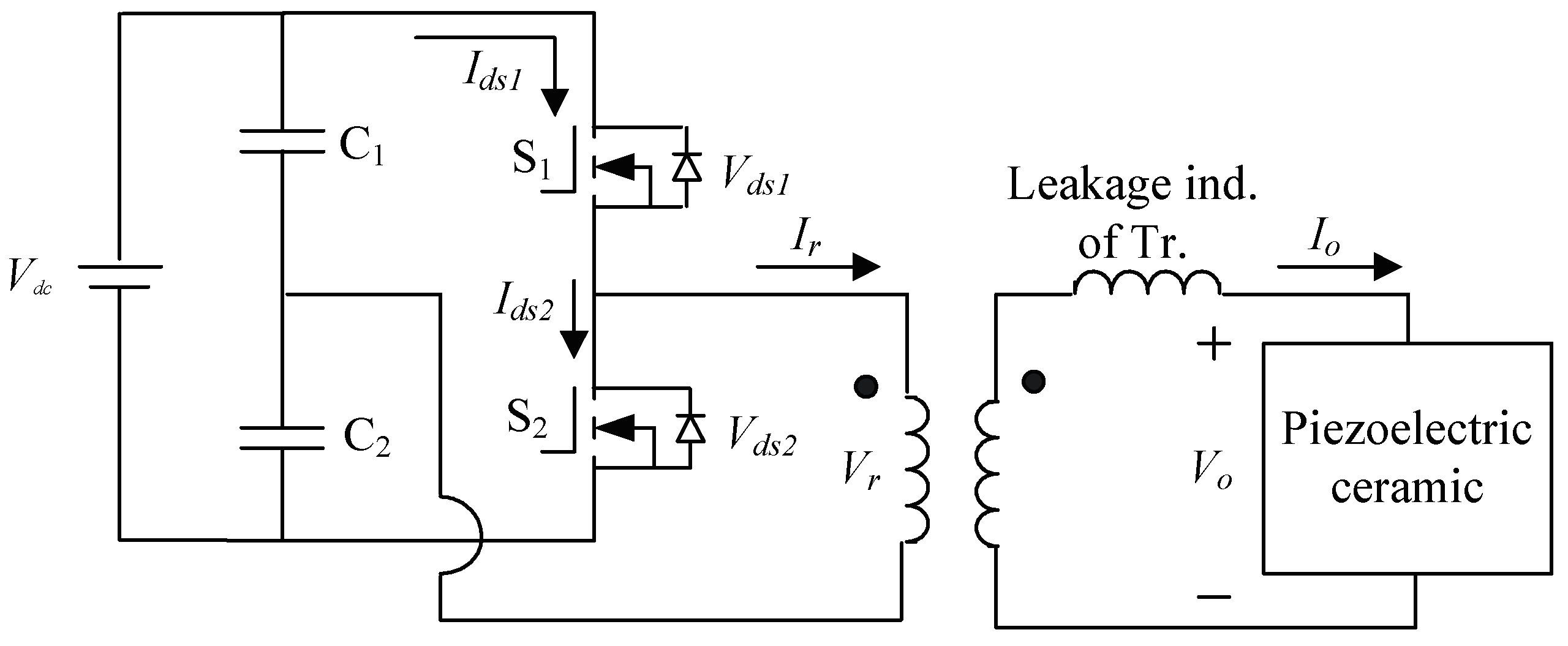
Figure 5 shows the proposed circuit configuration. In this circuit, power switches S1 and S2 are complementarily triggered under a symmetrical pulse width modulation control so that the input DC voltage of the inverter can be sharped to the square wave of voltage. This square wave is boosted by the transformer to drive the piezo ceramic. The amplitude of squared voltage is regulated by varying duty ratios of power switches. As shown in the figure, the magnitude of voltage waveform highly depends on the duty ratios of power switches D. The voltage function can be written as:
By Fourier analysis, Equations (7) and (8) can be expressed as below.
The fundamental component of resonant voltage Vr1(t) and its rms voltage is thus obtained:
In (11) and (12), the voltage gain shows a relation to the duty ratio D, where the maximum voltage appears at 0.5. The fundamental frequency of input current at resonant bank at ωo is:
The driving current at the switching moment is derived:
Equations (14) and (15) indicate that the magnitudes of Ids1-on and Ids2-on depend on the phase angle ψ. Now, if given a proper frequency, the piezo ceramics will behave like an inductor. Then a negative current is initially generated and goes through the diode D1(D2) of switch S1(S2). At this time, the current flows through the diode while the ZVS requirement is reached.
3.2. Propose Control Method
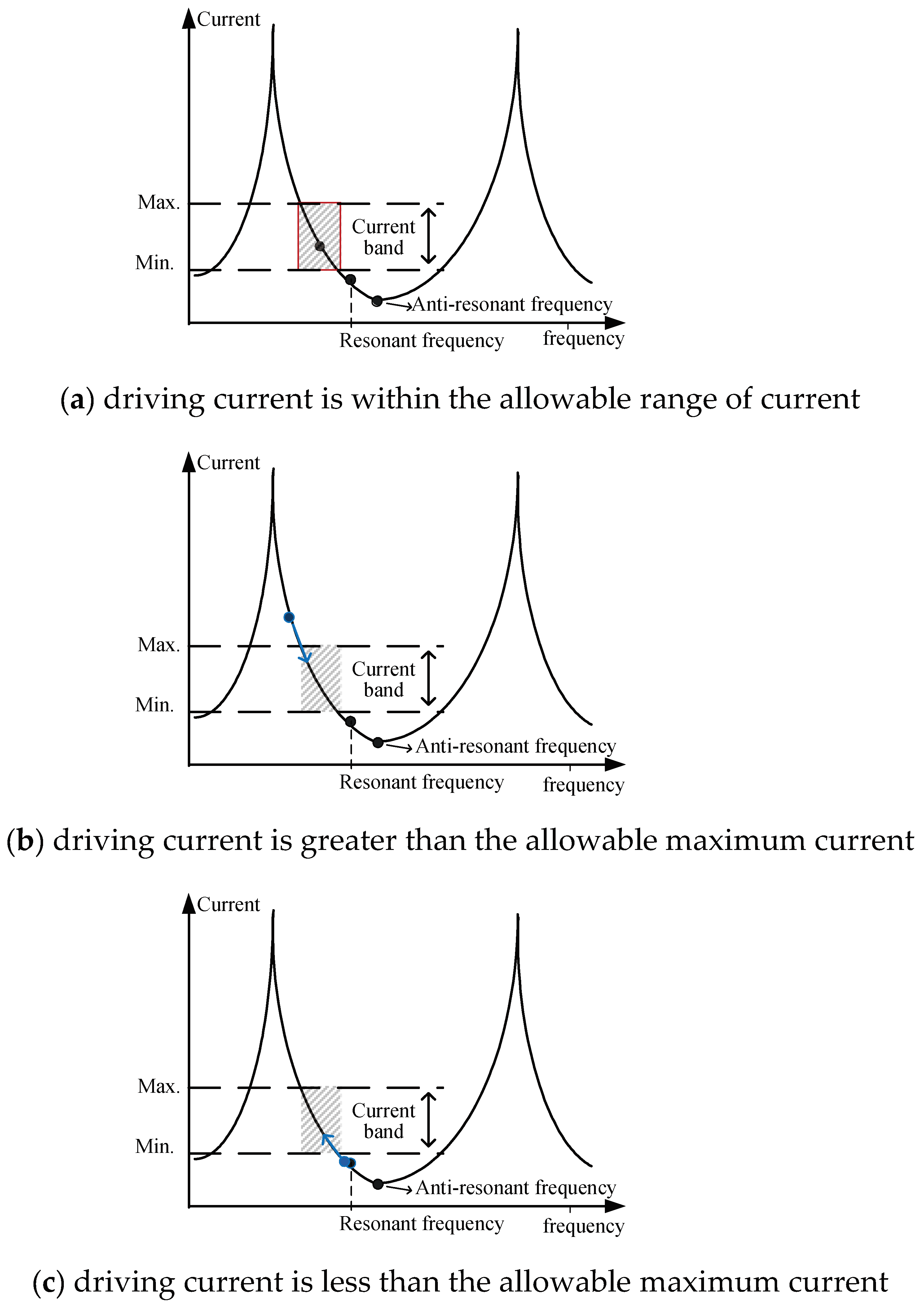
In this paper, the developed frequency control method is based on the current versus frequency characteristics of piezo ceramics. As shown in Figure 6a, when the operating frequency of the power driver is in the left of the resonant frequency, the piezo ceramic produces mechanical vibration, and a single frequency corresponds to a single current. That is, when the piezo-ceramic current is within the allowable range, the operating frequency will be close to the resonance point of the piezo ceramic. At this time, the driver can output sufficient power to produce mechanical vibration. There is thus no need to change the driving frequency. By increasing or decreasing the duty ratio of the power switch at the driver, the current or power control can be achieved. However, when the piezo-ceramic status changes, the proper frequency point of the circuit would change. As shown in Figure 6b, the current that corresponds to the original frequency exceeds the upper limit of the current setting, which shows that the frequency has deviated from the range of the resonant frequency. Therefore, the power driver needs to speed up the switching frequency to suppress the current and make the operating frequency closer to the resonance frequency. On the other hand, as shown in Figure 6c, if the current corresponding to the operating frequency is too small, the switching frequency should be reduced to increase the output current of the piezo-ceramic driver for maintaining a stable resonance.
Based on those ideas, the control flowchart is plotted in Figure 7.At the beginning of the control process, the output current is measured to confirm it can reach the allowable current level. If the output current is less or greater than the preset current, the controller will adjust the switching frequency according to the rules in Figure 6. That is, exceeding the upper limit set by the current, the proposed controller will increase the switching frequency fop to make the operating frequency closer to the resonant frequency. Instead, the switching frequency will be reduced. In addition, if the input voltage or temperature changes or other uncertainties in the circuit occur, there is an unexpected change in the operating power of the piezo-ceramic load. In this case, the constant output power procedure will be executed. As shown in Figure 7, this study uses a voltage- and current-detecting circuit, which can calculate the instantaneous driving power po. Then if the output power is higher than the preset power pset, the controller will reduce the PWM duty cycle of power switches (d − Δd), thereby reducing the power output. In contrast, if the output power is lower than the preset power, the control circuit will increase the duty cycle (d + Δd). These adjustments to the duty cycle will continue until the power signal is within the preset range. Note that when the circuit is started, an initial frequency is sent from the controller to make the driving circuit run first. The output current of the driver is then fed back after the circuit stabilizes. At this time, the power driver will judge the piezo-ceramic status and adjust the proper operating frequency. Usually, the initial frequency is intentionally set closer to the resonance frequency range of piezo ceramics. In this way, the possible excessive starting current can be suppressed by using the resonance characteristic of the circuit. The problems caused by overcurrent of the power driver during startup can be avoided.
4. Experimental Results
In order to investigate the feasibility of the proposed circuit, a hardware prototype was also implemented and tested in the laboratory. The experiment circuit diagram is shown in Figure 8. In this design, the AC input voltage in the circuit varies between 100 V and 120 V. In this circuit, a rectifier is employed for rectifying the ac power, and the dc capacitor bank (C1, C2) is for storing the rectified power and powering the inverter circuit. Since the inverter is directly connected to the dc capacitor bank, the PWM signal from the controller has to be isolated from the power source. Thus, another photo transistor TLP250H is added to the circuit to prevent the PWM signal from going directly to the inverter circuit, yet still allowing it to retain control of the MOSFET. At this stage, the current and voltage measurements of the load are performed by current transformer (CT) and voltage transformer (PT). The current and voltage signals are fed to a microcontroller PIC16F4520 so that the control algorithm in Figure 7 can be implemented. After the PWM switching of MOSFETs, the amplitude of the output voltage of the inverter is approximately 80 V. The driven piezoelectric ceramic is connected to an ultrasonic welding system to quantify the mechanical vibration caused by the proposed piezo-ceramic driver. An infrared device is used to measure the displacement of piezoelectric ceramics.
4.1. Drive Circuit Responses
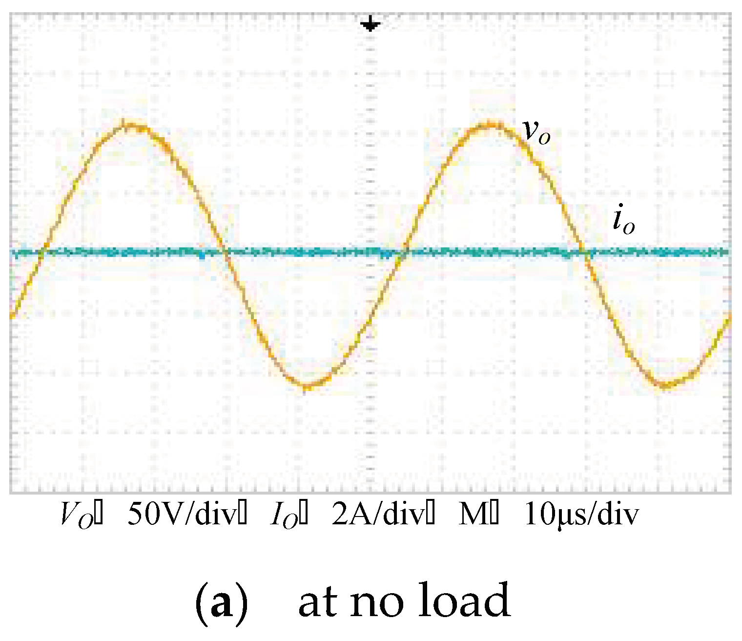
This test is aimed at examining the circuit response to different loads. The test waveform is obtained when the ac input voltage is fixed at 100 V. Figure 9 depicts the test results of different load conditions, where the output voltage of the resonant circuit is seen well stabilized under different scenarios. In the test, the voltage amplitude is measured at 77.8 V at no load, 78.8 V at a half load and 80.6 V at full-load conditions. This result helps verify that the proposed circuit can serve as a voltage source.
Next, the study has also tested the prototype circuit with its application to the constant power control under 100 VA and 200 VA. Figure 10 and Figure 11 depict these experimental waveforms, in which a sinusoidal output voltage is obtained after the circuit operates. In all test cases, the phase angle of voltage clearly leads the current with a high turn-ratio transformer connected, signifying that each switch in the inverter is activated before its current becomes positive and confirming that the power driver effectively performs the ZVS operation. In addition, as seen from the waveform of the triggering signal, the controller reduces the length of duty cycle when the load changes from 30 to 20 ohm. In this way, a different voltage gain can be grabbed to stabilize the output voltage and ensure that the power output of the circuit is less affected by the change of loads. In this test, the input and output powers are measured at 112.8 W and 103.3 W for the load of 30 ohm and at 222.3 W and 204.5 W for the load of 20 ohm. The circuit efficiencies are 91.6% and 92%. These test results show that the ZVS operation in the inverter is beneficial for reducing the power losses of the proposed inverter.
4.2. Piezo-Ceramic Tests
This test is focused on the circuit verification for the ultrasonic welding application. To carry out the test, the input voltage is set at 100 and 120 volts. This ensures that the waveforms of ceramic current and voltage are measured under the different dc-source voltages. Figure 12 depicts the experimental results, where the phase angle of voltage leads that of the current, indicating that the piezo ceramics can be viewed as an inductive load. Meanwhile, as the circuit is not influenced by the variation of input ac voltage, the output voltage waveform for each case can be maintained almost the same. Figure 13 shows the displacement of the ultrasonic welding joint under the tests. The measurement results show that the maximum displacement is near 0.075 mm. The generated displacement is sufficient to rapidly weld the plastic, thus verifying the practicability of the proposed method.
5. Conclusions
In this paper, a new driving circuit is proposed for piezo ceramics. One of the most crucial contributions of this circuit is the application of transformer leakage to flatten the voltage gain curve of the piezo-ceramic driver over the resonant frequency range, so voltage gain changes are insensitive to frequency changes. Then, the frequency and power tracking schemes are developed based on the on-line switching frequency and duty ratio adjustments. Thus, the piezo-ceramic vibration is well controlled. Currently, the concepts of the study are being extended to implement a large-scale driving circuit for an ultrasonic welding system.
Author Contributions
Conceptualization, F.-S.P.; methodology, F.-S.P.; software, H.-L.H.; validation, F.-S.P. and H.-L.H.; formal analysis, F.-S.P.; investigation, F.-S.P.; resources, F.-S.P.; data curation, F.-S.P.; writing—original draft preparation, F.-S.P. and H.-L.H.; writing—review and editing, F.-S.P.; visualization, H.-L.H.; supervision, F.-S.P.; project administration, F.-S.P.; funding acquisition, F.-S.P. All authors have read and agreed to the published version of the manuscript.
Funding
This work was supported by the National Science and Technology Council, Taiwan, under project MOST 111-2221-E-024-004.
Data Availability Statement
The data presented in this study are available on request from the corresponding author.
Acknowledgments
The authors are greatly indebted to Senior Engineers Yi-Fu Ou and Jia-In Lin at AUO Corporation for providing their valuable operating experiences.
Conflicts of Interest
The authors declare no conflict of interest.
References
- Jittakort, J.; Sangswang, A.; Naetiladdanon, S.; Koompai, C.; Chudjuarjeen, S. Full bridge resonant inverter using asymmetrical control with resonant-frequency tracking for ultrasonic cleaning applications. J. Power Electron. 2017, 17, 1150–1159. [Google Scholar]
- Keawboonchuay, C.; Engel, T. Maximum power generation in a piezoelectric pulse generator. IEEE Trans. Plasma Sci. 2003, 31, 123–128. [Google Scholar] [CrossRef]
- Juang, P.-A.; Tsai, C.-C. Equivalent Circuit Modeling of an Asymmetric Disc-Type Ultrasonic Motor. IEEE Trans. Instrum. Meas. 2009, 58, 2351–2357. [Google Scholar] [CrossRef]
- Zhang, Q.; Piao, S.C.; Chen, H.J.; Wu, J.; Nakamura, K. A linear piezoelectric actuator using a-shaped Structure. IEEE Trans. Ultrason. Ferroelectr. Freq. Control 2022, 69, 1382–1391. [Google Scholar] [CrossRef] [PubMed]
- Tsujino, J.; Hongoh, M.; Yoshikuni, M.; Miura, H.; Ueoka, T. Welding characteristics and temperature rises of various frequency ultrasonic plastic welding. In Proceedings of the IEEE Ultrasonics Symposium, Rotterdam, The Netherlands, 18–21 September 2005; Volume 1, pp. 707–712. [Google Scholar]
- Cheng, L.-C.; Kang, Y.-C.; Chen, C.-L. A Resonance-Frequency-Tracing Method for a Current-Fed Piezoelectric Transducer. IEEE Trans. Ind. Electron. 2014, 61, 6031–6040. [Google Scholar] [CrossRef]
- Cheng, C.A.; Cheng, H.L.; Chang, E.C.; Chang, C.H.; Tsai, C.Y.; Lan, L.F. A novel drive circuit for supplying piezoelectric ceramic actuator with power-factor-correction and soft-switching features. In Proceedings of the IEEE International Future Energy Electronics Conference, Taipei, Taiwan, 16–19 November 2021; pp. 1–4. [Google Scholar]
- Agbossou, K.; Dion, J.-L.; Carignan, S.; Abdelkrim, M.; Cheriti, A. Class D amplifier for a power piezoelectric load. IEEE Trans. Ultrason. Ferroelectr. Freq. Control 2000, 47, 1036–1041. [Google Scholar] [CrossRef] [PubMed]
- Amir, S.; van der Zee, R.; Nauta, B. A Self-Oscillating Boosting Amplifier With Adaptive Soft Switching Control for Piezoelectric Transducers. IEEE J. Solid-State Circuits 2019, 54, 253–265. [Google Scholar] [CrossRef] [Green Version]
- Wang, J.-D.; Jiang, J.-J.; Duan, F.-J.; Cheng, S.-Y.; Peng, C.-X.; Liu, W.; Qu, X.-H. A High-Tolerance Matching Method against Load Fluctuation for Ultrasonic Transducers. IEEE Trans. Power Electron. 2020, 35, 1147–1155. [Google Scholar] [CrossRef]
- Liu, X.; Colli-Menchi, A.I.; Gilbert, J.; Friedrichs, D.A.; Malang, K.; Sanchez-Sinencio, E. An Automatic Resonance Tracking Scheme With Maximum Power Transfer for Piezoelectric Transducers. IEEE Trans. Ind. Electron. 2015, 62, 7136–7145. [Google Scholar] [CrossRef]
- Jiang, X.; Zhu, X.B.; Wong, C.Y.; Zhang, D.; Geng, D. Theory of series inductance matching to transducer at pre-mechanical resonance zone in ultrasonic vibration cutting. IEEE Trans. Ind. Electron. 2019, 66, 3019–3029. [Google Scholar] [CrossRef]
- Tang, S.C.; Clement, G.T. A harmonic cancellation technique for an ultrasound transducer excited by a switched-mode power converter. IEEE Trans. Ultrason. Ferroelectr. Freq. Control 2008, 55, 359–367. [Google Scholar] [CrossRef] [PubMed]
Figure 1.
Equivalent circuit of a piezo ceramic.

Figure 2.
Resonant characterization of a piezo ceramic.

Figure 3.
Drive schematic diagram for a piezo ceramic.

Figure 4.
Voltage gain plot of the piezo ceramic under different series inductances.

Figure 5.
Proposed circuit configuration.

Figure 6.
Proposed frequency control method.

Figure 7.
Flow chart of the proposed control method.

Figure 8.
The experiment circuit diagram.

Figure 9.
The experimental voltage and current waveforms under different resistive loads.


Figure 10.
100 VA tests for constant power control.

Figure 11.
200 VA tests for constant power control.

Figure 12.
Voltage and current waveforms of the proposed driver for the ultrasonic welding application.
Figure 12.
Voltage and current waveforms of the proposed driver for the ultrasonic welding application.

Figure 13.
Displacement joint for the ultrasonic welding application.

Disclaimer/Publisher’s Note: The statements, opinions and data contained in all publications are solely those of the individual author(s) and contributor(s) and not of MDPI and/or the editor(s). MDPI and/or the editor(s) disclaim responsibility for any injury to people or property resulting from any ideas, methods, instructions or products referred to in the content. |
© 2023 by the authors. Licensee MDPI, Basel, Switzerland. This article is an open access article distributed under the terms and conditions of the Creative Commons Attribution (CC BY) license (https://creativecommons.org/licenses/by/4.0/).
Share and Cite
MDPI and ACS Style
Pai, F.-S.; Hu, H.-L. Driving Circuit Design for Piezo Ceramics Considering Transformer Leakage Inductance. Processes 2023, 11, 247. https://0-doi-org.brum.beds.ac.uk/10.3390/pr11010247
AMA Style
Pai F-S, Hu H-L. Driving Circuit Design for Piezo Ceramics Considering Transformer Leakage Inductance. Processes. 2023; 11(1):247. https://0-doi-org.brum.beds.ac.uk/10.3390/pr11010247
Chicago/Turabian StylePai, Fu-Sheng, and He-Lin Hu. 2023. "Driving Circuit Design for Piezo Ceramics Considering Transformer Leakage Inductance" Processes 11, no. 1: 247. https://0-doi-org.brum.beds.ac.uk/10.3390/pr11010247
Note that from the first issue of 2016, this journal uses article numbers instead of page numbers. See further details here.