
Modified SPWM Control for a Single-Stage Differential Boost Inverter Applied in a BESS


1
Department of Electrical Engineering, National Taiwan University of Science and Technology, Taipei 106335, Taiwan
2
Chung-Shan Institute of Science and Technology, Taoyuan City 325204, Taiwan
3
Undergraduate Program of Vehicle and Energy Engineering, National Taiwan Normal University, Taipei 106308, Taiwan
*
Author to whom correspondence should be addressed.
Processes 2021, 9(11), 1861; https://0-doi-org.brum.beds.ac.uk/10.3390/pr9111861
Submission received: 2 August 2021
/
Revised: 6 October 2021
/
Accepted: 15 October 2021
/
Published: 20 October 2021
(This article belongs to the Special Issue Application of Power Electronics Technologies in Power System)
Abstract
:This study aims to implement a single-stage differential boost inverter (SSDBI) applied in a single-stage battery energy storage system (BESS) topology that can supply power from a lower-voltage battery module to an alternating current (AC) load. Compared with the common two-stage topology, which has a two-stage converter and higher-voltage battery module array, the single-stage topology can reduce the number of cells and components and improve the power density. In addition, a modified sinusoidal pulse-width modulation (SPWM) control was proposed to reduce the control complexity of the SSDBI while improving the total harmonic distortion (THD) of the inverter. The modified SPWM control can reduce the duty ratio of the SSDBI and the stress on the components in order to improve the AC voltage output waveform and reduce the THD.
1. Introduction
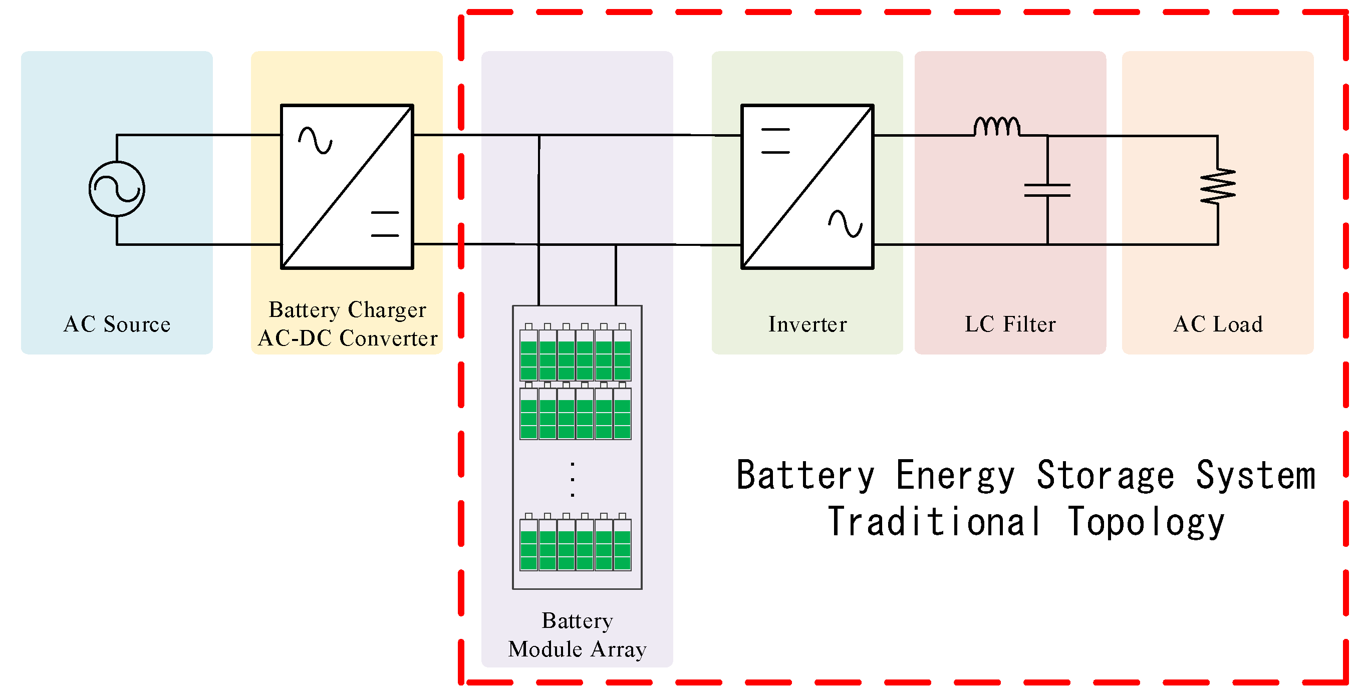
Nowadays, the technology of inverters has been increasingly developed because they are widely used in numerous applications, such as in PV and power grids. Inverters and battery storage systems are some of the most popular combinations. The inverter plays an important role in a BESS, where the inverter is responsible for the energy transmission. Figure 1 shows the most familiar block diagram of a BESS, which includes a battery module array, a battery charger, and an inverter [1,2,3]. First, the AC source (utility power) can charge the battery pack through the battery charger. Next, the inverter can extract the energy from the battery pack to the AC load. Finally, the battery pack is responsible for the whole power supply when the AC source is removed.
However, it does not make economic sense to use the BESS structure shown in Figure 1. The first reason is that a single cell’s voltage is quite low. For example, the voltages of lead–acid, Ni-Cd, and lithium-ion batteries are 2.0, 1.2, and 3.7 V, respectively. A common BESS also needs high voltage, such as 380–400 Vdc, for the inverter to supply power to the AC load. Under this condition, the battery module array should be composed of numerous cells connected in series. A high-voltage battery module array will also lead to another problem, which is the cell state of charge (SOC) imbalance. If the imbalance problem occurs, some of the cells will be overcharged or over-discharged as a result of long-term work. Their state of health (SOH) will also decrease, and can even be permanently damaged [4,5,6]. Furthermore, the battery management system (BMS) will be more difficult, more expensive, and more dangerous when the battery module array’s voltage becomes higher.
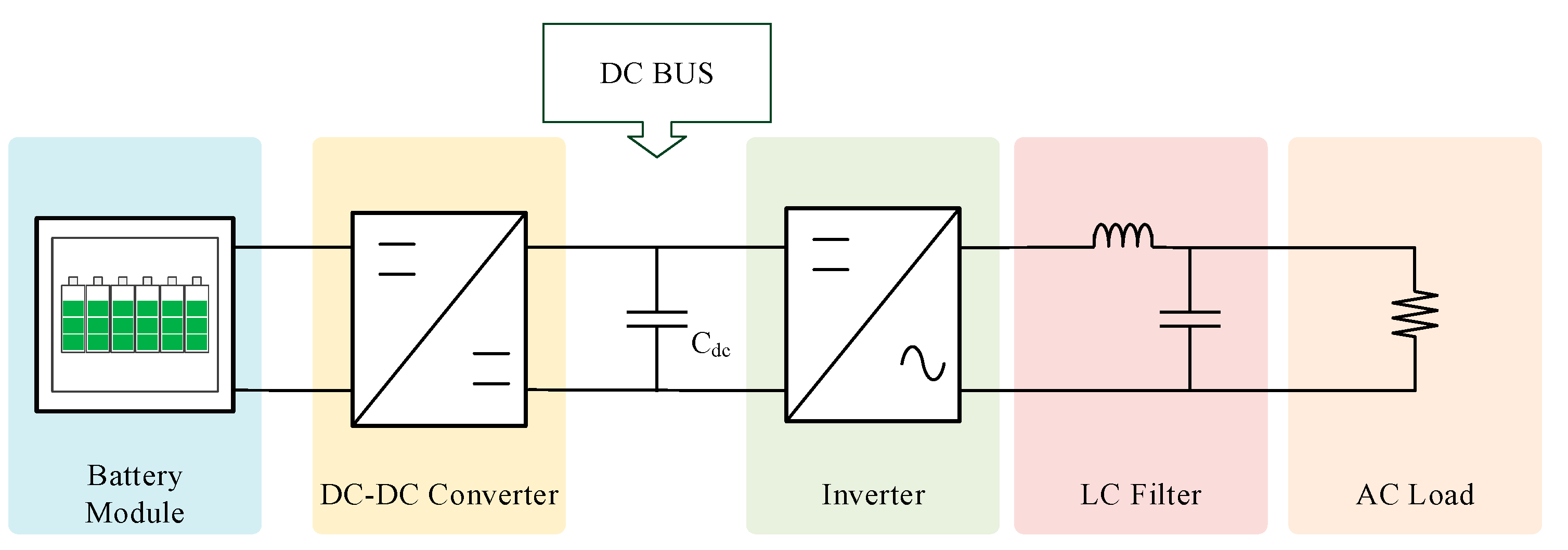
To overcome the aforementioned problem, the two-stage topology has been proposed [7,8]. The structure includes a battery module, a DC-DC converter, an inverter, DC bus capacitors, and AC load, as shown in Figure 2. The topology uses a battery module with an additional DC-DC boost converter instead of a high-voltage battery module array. However, large DC bus capacitors are a must for these topologies in order to connect the DC-DC converter with the inverter. Compared with the traditional topology, the two-stage topology is easy to implement and has quite mature technology in spite of the number of the components, their short lifetime, and large size.
Figure 3 displays the Pseudo DC-link topology, which includes a low-voltage battery module, DC-DC converter, inverter, and AC load [9,10]. The difference between the two-stage topology and Pseudo DC-link topology is the switch operation of the DC-DC converter. The switching control signal of the DC-DC converter in the Pseudo DC-link topology is based on sinusoidal pulse width modulation (SPWM) instead of traditional pulse width modulation (PWM). Therefore, in the Pseudo DC-link topology, the output of the DC-DC converter and the input of the inverter are a rectified sinusoidal waveform. The topology can convert the low voltage of the battery module into a rectified sinusoidal waveform with the DC-DC converter. The voltage of the rectified sinusoidal waveform is high enough for the inverter to supply power to the AC load. The Pseudo DC-link topology can overcome the need for large capacitors in the traditional two-stage topology. In addition, the operation efficiency of the inverter will increase because of the switching frequency reduction. Nevertheless, the Pseudo DC-link topology is still a two-stage topology in which plenty of the components are the same as those in the traditional two-stage topology.
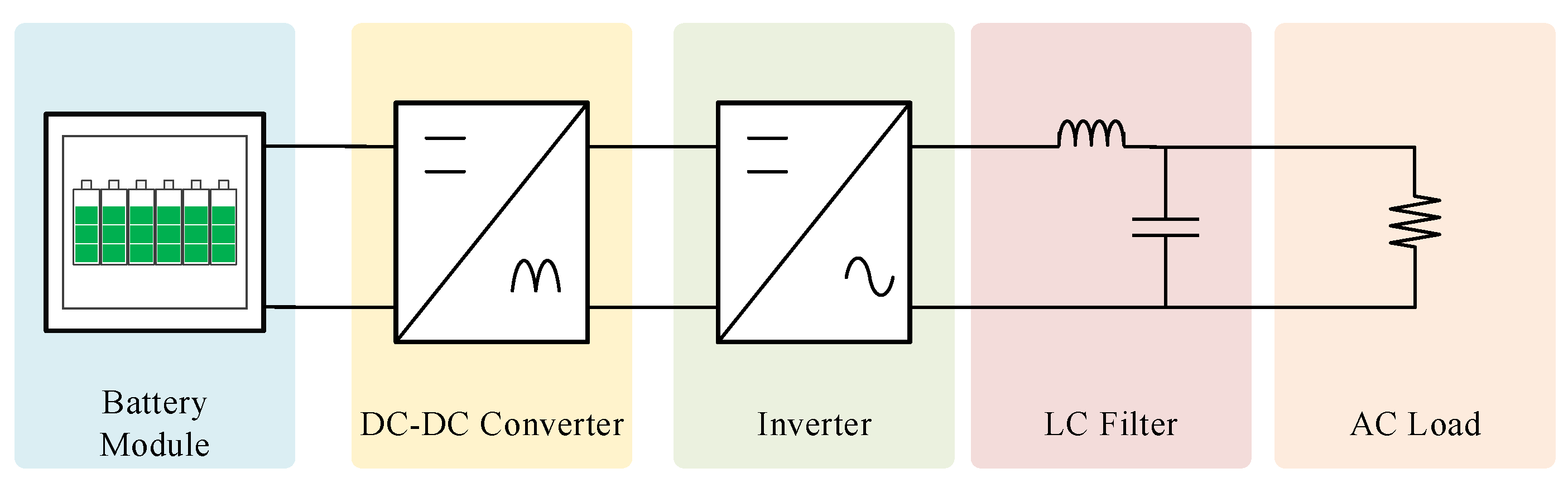
For further improvement, the single-stage topology was proposed by recent research to minimize the components used [11,12]. Figure 4 shows the single-stage topology, which includes a battery module, a single-stage inverter, and an AC load. The single-stage inverter has good performance in adjusting the voltage and gives an AC output instead of a DC-DC converter and inverter combination. Compared with the two-stage topology, the single-stage inverter in the single-stage topology is not mature enough and is too complicated to implement.
This study proposes a single-stage inverter, as displayed in Figure 5, which is also called a single-stage differential boost inverter (SSDBI). Compared with the others [11,12], the purpose of the proposed inverter is to provide energy from a low-voltage battery module to a 110 Vac AC load, but while connected with the grid. The inverter has fewer components, which only include two inductors, two capacitors, and four switches. Due to the characteristics of the structure, the converter uses high-frequency inductors instead of filter inductors to reduce the cost and the size of the inductors. The capacitors are not used to store an amount of energy, so the capacitance and the size of the capacitors have a lower cost and are smaller.
In previous studies, researchers proposed controls based on the proposed single-stage inverter [13,14,15,16,17]. Damith B. Wickramasinghe Abeywardana and Woei-Luen Chen, respectively, proposed a control combining proportional integral control (PI control) with proportional resonant control (PR control). The control compensated the capacitor’s voltage with PR control and then the inductor’s current with PI control. This control had better AC voltage stability while adjusting and limit the inductor’s current. However, the control was a double-loop compensator, which made it difficult to stabilize both the outer loop and the inner loop [13,14]. Diana Lopez-Caiza and Oswaldo López-Santos separately proposed sliding-mode control (SMC). Through discontinuous control, SMC keeps adjusting the inductor’s current and the capacitor’s voltage until the inverter works in stable conditions. SMC is suitable for the SSDBI because it can individually control nonlinear current and voltage. SMC could also reduce the THD of the inverter, but the SMC needs plenty of feedback signals, and the design is also complicated. Kapil Jha used SPWM control, which simplified the design of the control at the cost of THD. Moreover, the control methods, such as space vector pulse width modulation (SVPWM) and the SPWM control with an additional third harmonic, have better utilization of the DC link voltage. However, these control methods are usually used in three-phase buck inverters for driving three-phase motors, and they regard the inverter and the motor as a whole to control the motor’s RPM by adjusting the voltage and frequency, but with a constant flux. The traditional SPWM control is not commonly used in real circuits when the load is a motor, but rather when loads have a constant frequency, such as in telecommunication base stations or uninterrupted power supplies.
In view of the above research, this study modified the SPWM for the SSDBI. Through a steady-state circuit analysis, simulations, and hardware experiments, this study verified the proposed inverter’s feasibility and the control’s modification while considering the system’s complication, cost, and THD.
2. System Description of SSDBI
This section describes the steady-state analysis of the SSDBI and the design considerations of the components.
2.1. Steady-State Analysis of the SSDBI
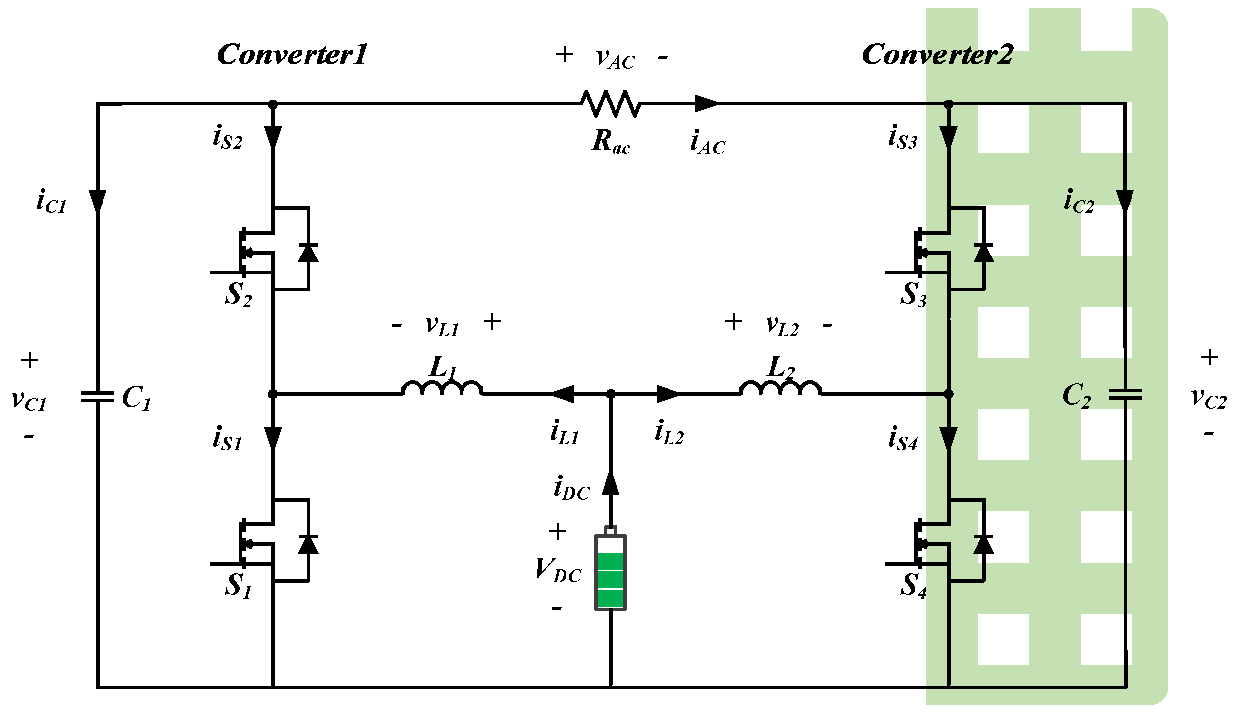
To simplify the analysis, the inverter can be separated into two parts, Converter 1 and Converter 2, because the inverter has a differential architecture. As shown in Figure 6, the directions and symbols of the loops’ current and voltage are defined and labeled, where VDC and iDC are the voltage and the current of the DC bus, vAC and iAC are the voltage and the current of the AC load, vL1 and iL1 are the voltage and the current of the inductor L1, vL2 and iL2 are the voltage and the current of the inductor L2, vC1 and iC1 are the voltage and the current of the capacitor C1, and vC2 and iC2 are the voltage and the current of the capacitor C2. According to Kirchhoff’s Voltage and Current Law, iDC is equal to the sum of iL1 and iL2, and vAC is equal to the difference of vC1 and vC2.
Since the switching frequency of the inverter is much higher than that required by the AC load, the inverter will perform multiple charging and discharging cycles with the switching frequency in a period of the AC load. Therefore, the following will be introduced with a positive half period and a negative half period, respectively. Table 1 shows the operation modes of Converter 1 and Converter 2, and Figure 7 displays the operation states of the inverter. In the positive half period (vAC > 0), Converter 1 works as a boost converter that charges C1 with vDC, and Converter 2 works as a buck converter that charges VDC. In the negative half period (vAC < 0), Converter 1 works as a buck converter that charges VDC, and Converter 2 works as a boost converter that charges C2. Both Converter 1 and Converter 2 have opposite but similar operation modes in the positive (Mode 1 and Mode 2) and negative (Mode 3 and Mode 4) half periods, respectively. For the steady-state analysis, the positive half period (Mode 1 and Mode 2) will be taken as an example.
Mode 1 [t0~t1]:
In Mode 1, , . S1 (on), S2 (off), S3 (on), and S4 (off). L1 and L2 are being charged and C1 and C2 are discharging. The voltage across L1 is , and the voltage across L2 is. The current passed by C1 is , and that passed by C2 is . The variations in each of the inductors’ current and capacitors’ voltage can be obtained as follows:
Mode 2 [t1~t2]:
In Mode 2, , . S1 (off), S2 (on), S3 (off), and S4 (on). L1 and L2 are discharging, and C1 and C2 are being charged. The voltage across L1 becomes , and the voltage across L2 becomes . The current passed by C1 changes to , and that passed by C2 changes to . The variations in each of the inductors’ current and capacitors’ voltage are as follows:
Through the aforementioned analysis, Equations (9) and (10) can be obtained by referring to (1), (2), (5), (6), and the volt-second balance theory.
We already know that vAC is equal to the voltage difference between vC1 and vC2. Hence, the relationship between VDC and vAC can be calculated in (11).
After rearranging (11), the duty ratio D is expressed as follows:
The gain of the inverter M is the ratio of VDC and vAC. Rearranging (12) once more, M and the relationship between M and D can be shown by the following.
2.2. Design Considerations of the Components
Through the analysis, it can be observed that the formula of Converter 1 in the positive half period is the same as the formula of Converter 2 in the negative half period. So, the capacitances of C1 and C2 are the same. Therefore, the design formula of C1 and C2 can be inferred from (3), as shown in (15), where is the ripple of the capacitor’s voltage.
In addition, the design considerations of the inductors are similar to those of the capacitors. The formula of the design considerations can be inferred from (1), as shown in (16), where is the ripple of the inductor’s current.
3. The Analysis of the Control
3.1. The Problem of Applying Traditional SPWM Control to the Proposed Inverter
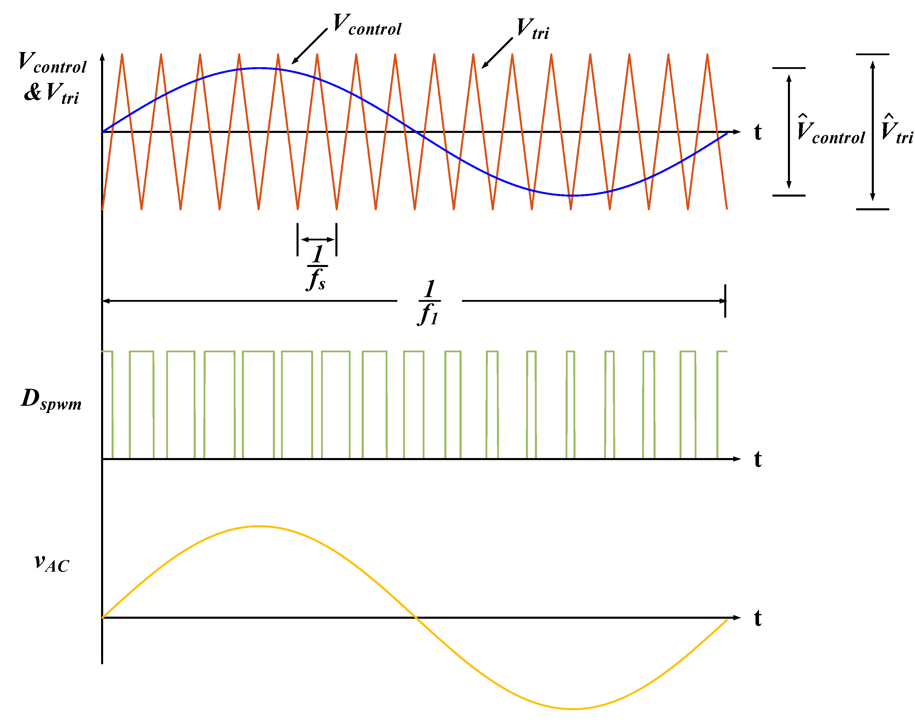
It is well known that there have already been many types of control proposed for inverters; SPWM is the most mature one of these, and this type of control is usually applied for buck inverters. Figure 8 shows the traditional SPWM control principle applied to a buck inverter, where the duty ratio Dspwm is generated by the comparison between a sine wave signal Vcontrol and a triangular wave signal Vtri, the amplitude and frequency of Vtri are and fs, represents the amplitude of Vcontrol, and the sine wave’s frequency f1 is the same as the output voltage frequency f [18].
The amplitude modulation index ma is the ratio of and . ma can determine Dspwm, as shown in (17).
Since SPWM is mainly used in buck inverters, the gain M must be less than 1, which is half of ma. The formulas of M and the rearranged Dspwm are shown in (18) and (19).
If the DC voltage is assumed as a stable power supply, its value will be constant. Through the aforementioned formula, Dspwm, vAC, and M will increase while Vcontrol (t) increases. So, can be regarded as vAC (t) with an equally scaled reduced amplitude. M has a linear relationship with Dspwm.
However, if the above SPWM control is directly used in the SSDBI [17], the voltage of the AC output will be distorted. As shown in Figure 9, the expected sinusoidal waveform of the AC output will become a waveform that is similar to a triangular waveform.
The reason for the distortion is that Vcontrol still has the same relationship with vAC, Dspwm, and Vcontrol. However, the formulas among these parameters, as shown in (12) and (14), are different from those of the buck inverter.
3.2. The Proposed Modified SPWM Control
To overcome this distortion, this study generated a modified SPWM control for the proposed inverter. The proposed SPWM modifies a new formula for the new duty ratio Dmodified_spwm, which can be obtained from (12).
We can get the modified Vcontrol (t) by putting (20) into (17), as shown in (21). Although Vcontrol has a new relationship with vAC, the inverter driven with Dmodified_spwm will have the expected sinusoidal voltage waveform of the AC output.
Figure 10 displays the comparison between the traditional SPWM control and the modified SPWM control. In Figure 10a, the comparison is focused on Vcontrol, where the dotted line and the solid line represent Vcontrol in the traditional SPWM control and the modified SPWM control, respectively. Figure 10b shows the voltage waveform’s difference in the AC output. According to Figure 10, even if the traditional SPWM control gives a sine wave signal for Vcontrol in the proposed inverter, vAC will be distorted. In contrast, the proposed SPWM control will have the expected sinusoidal voltage output with the modified Vcontrol.
4. Experimental Results
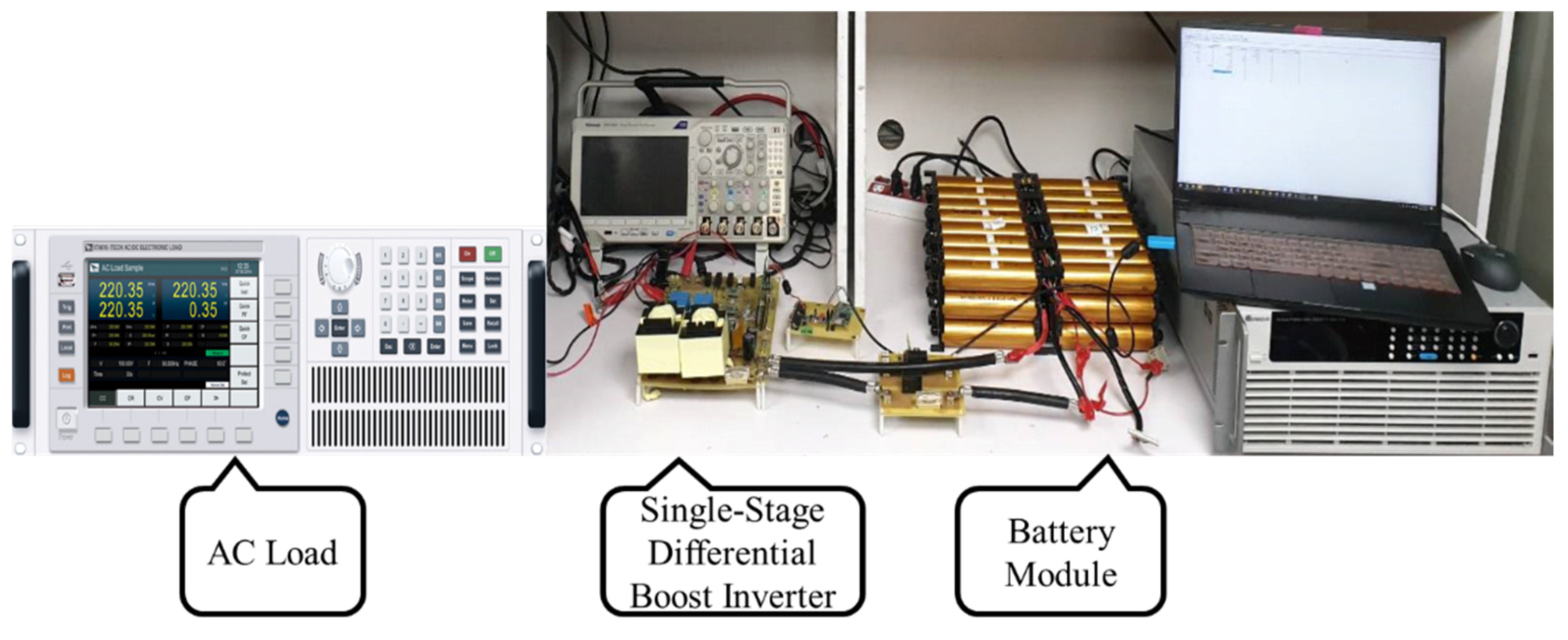
4.1. Description of System Specifications
Figure 11 shows the experimental platform of the SSDBI, and the actual system configuration is displayed in Figure 12. In this study, the DC input was a 16S3P battery module, where the single cells (PC40155) were manufactured by Phoenix Battery Corporation, and the voltage range of the battery module was 33.6–58.4 Vdc. The other system specifications can also be obtained in Table 2, for which the inductors and the capacitors were measured with an LCR meter (WK3255B).
4.2. Results of the Simulation and Hardware Experiments
In this section, the proposed modified control is compared with the traditional SPWM using the results of simulation and hardware experiments. The proposed BESS was tested under different test conditions; the AC loads used included: 48 Ω (250 W), 24 Ω (500 W), and 12 Ω (1 kW). The simulation software used in this research, Matlab, was manufactured by MathWorks, Inc. (Natick, MA, USA).
First, this study compared the controls’ influence on the output waveforms in simulations, as shown in Figure 13, where the traditional SPWM control is represented by a dotted line, the modified SPWM control is displayed with a solid line, the X-axis is for the time, and the Y-axis is the amplitude of Vcontrol. From Figure 13, it can be observed that Vcontrol of the modified SPWM was not a sinusoidal waveform.
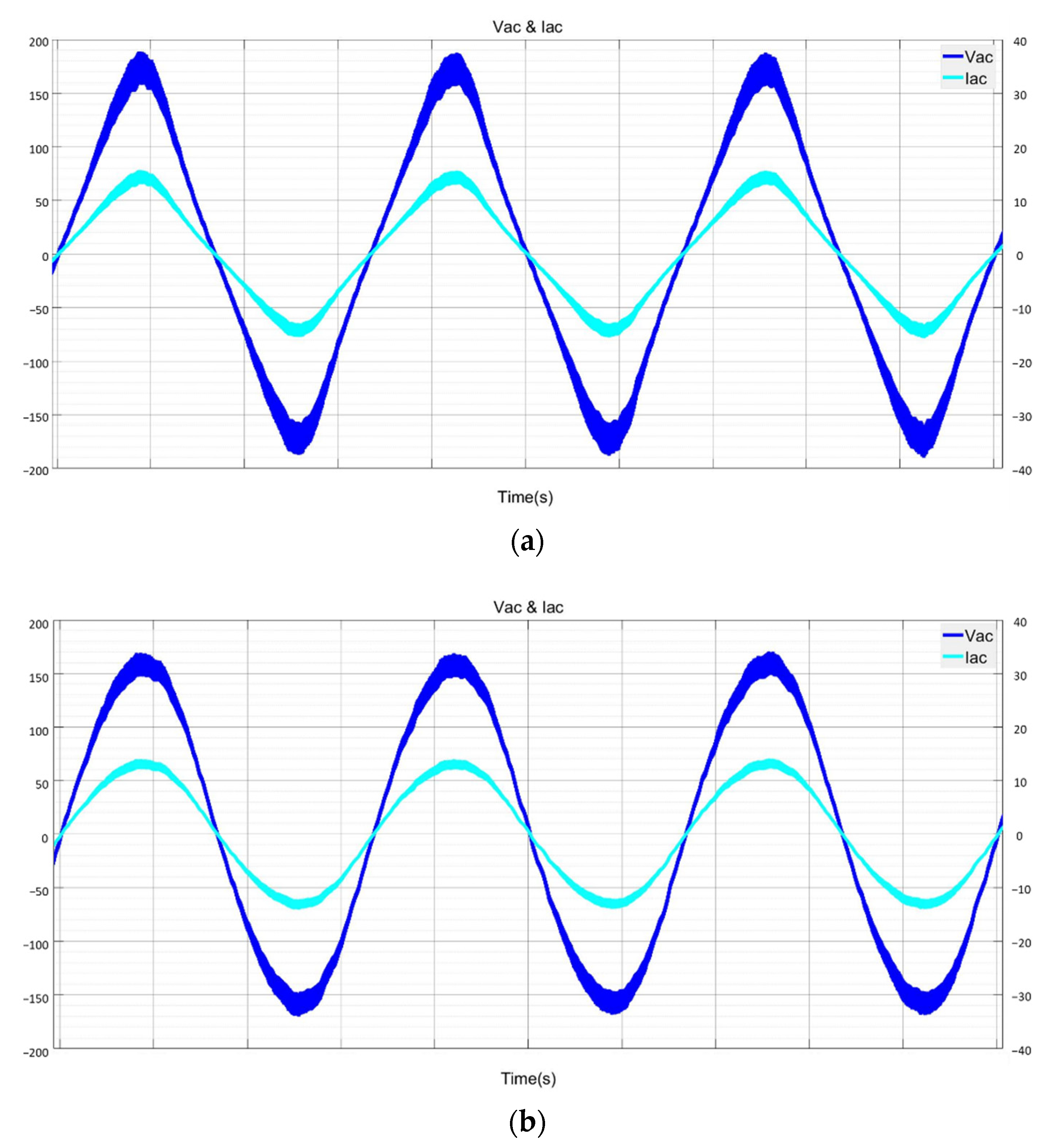
Secondly, the Vcontrol of both controls when applied to the control loop to drive the SSDBI in the simulations is shown in Figure 14. The output waveforms are displayed in Figure 15, Figure 16 and Figure 17, which show the voltage and current waveforms with the traditional SPWM control and the modified SPWM control. By analyzing the differences, it can be easily observed that the proposed inverter with the application of the modified SPWM control had a better output in the simulation.
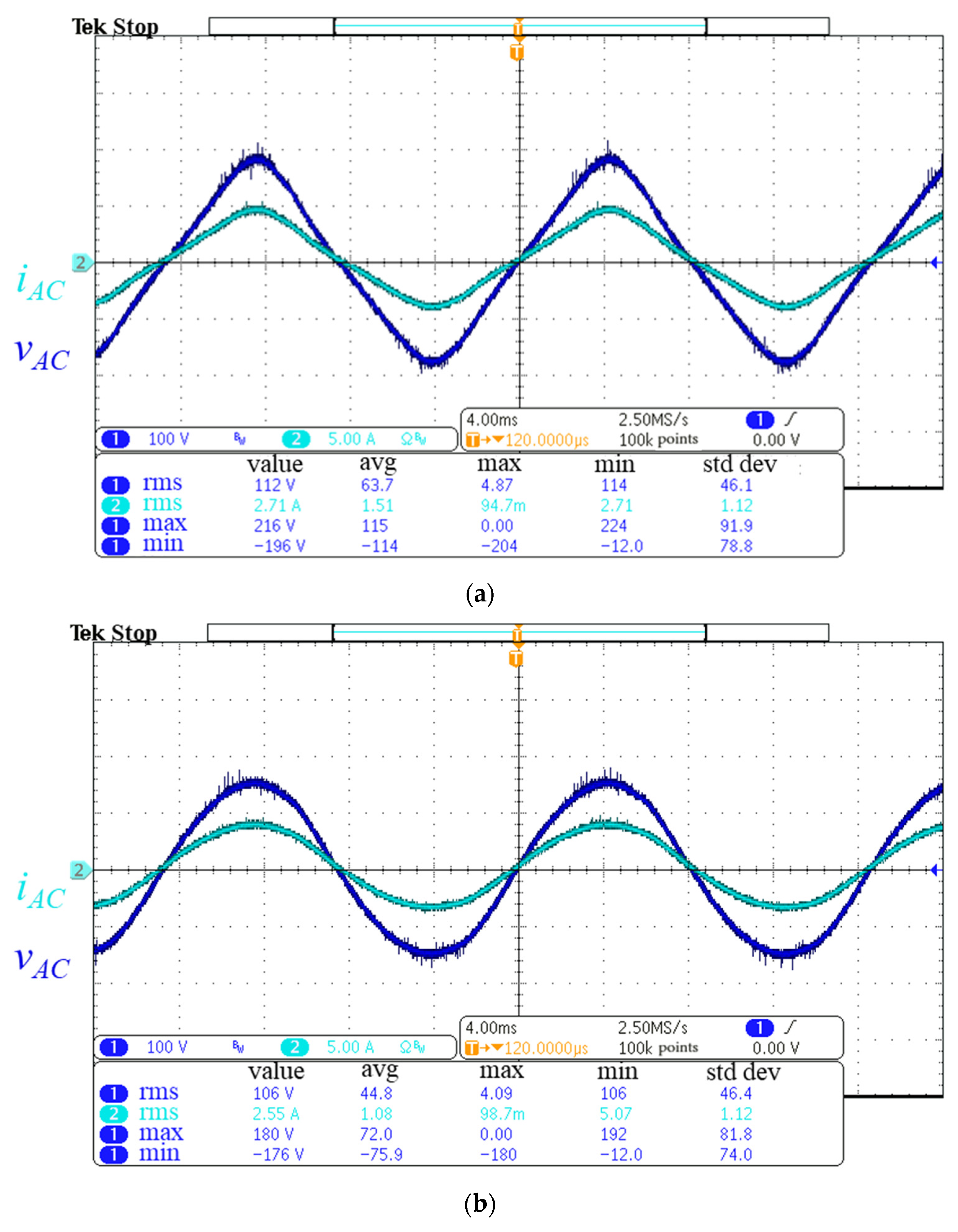
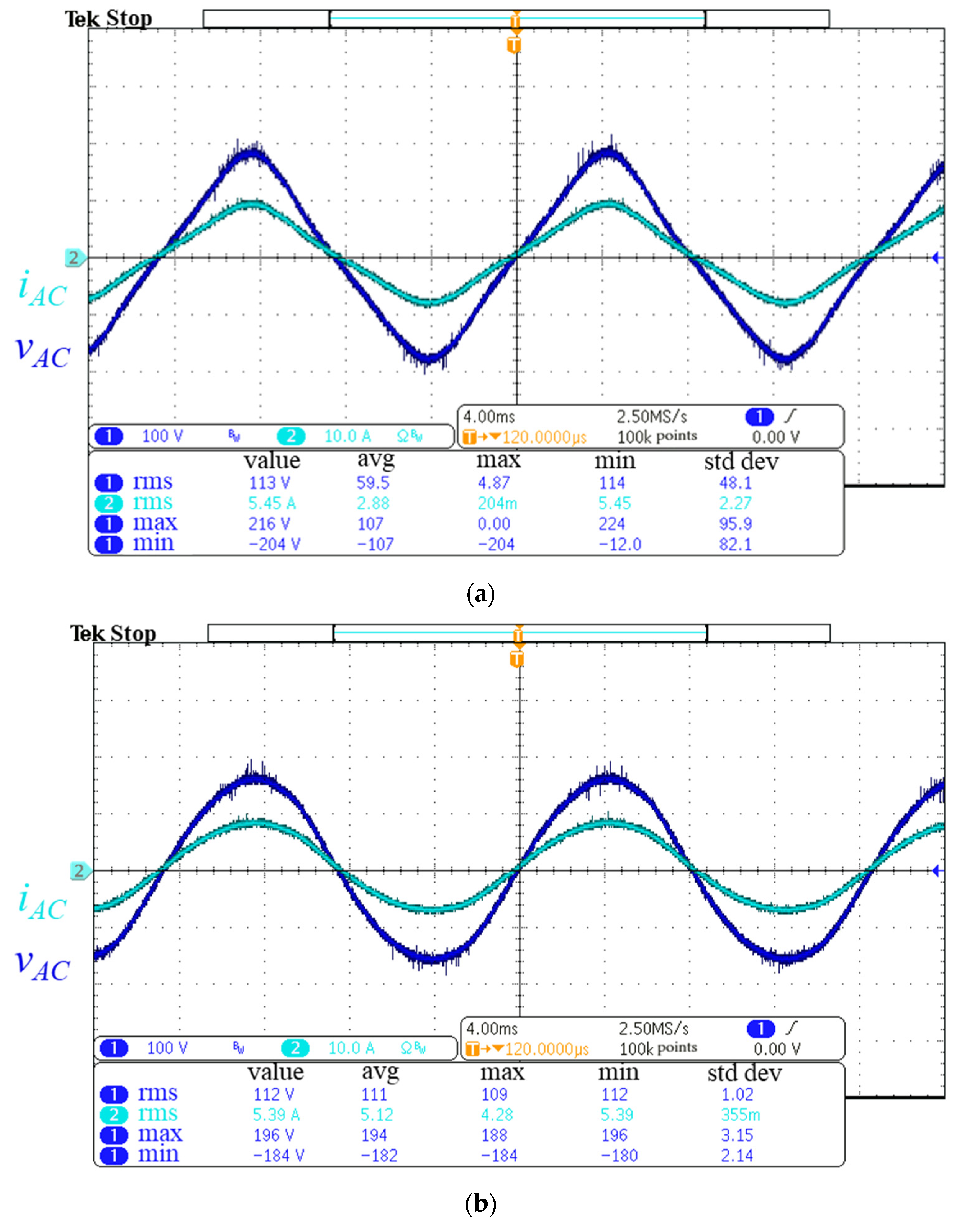
For further verification, this study tested the SPWM controls in hardware experiments. The waveforms from the hardware experiments are shown in Figure 18, Figure 19 and Figure 20. The results show that the traditional SPWM control needs a larger peak value of both the voltage and current than the modified control while reaching the same root mean square (RMS). This problem will lead to an increment in the system specifications.
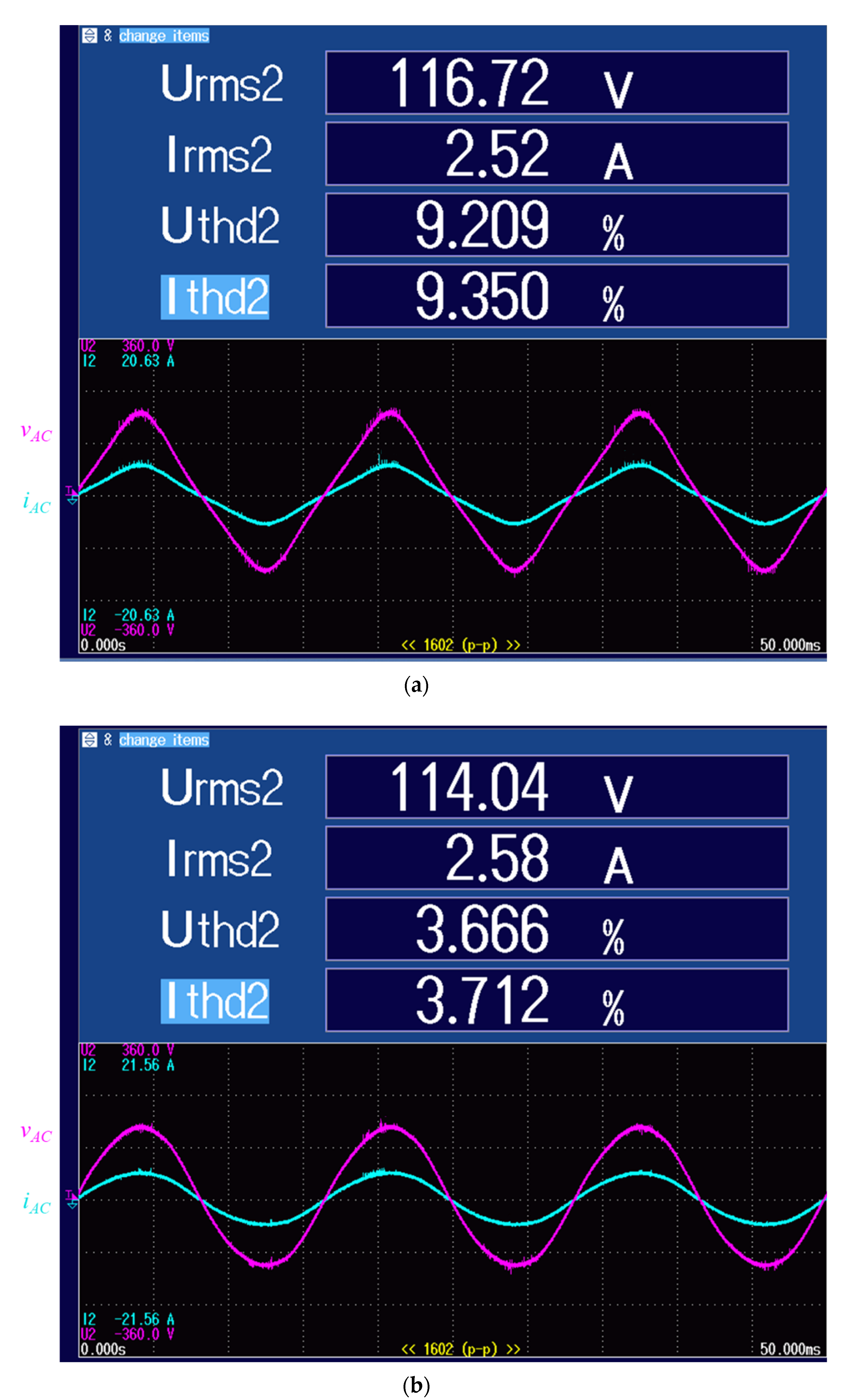
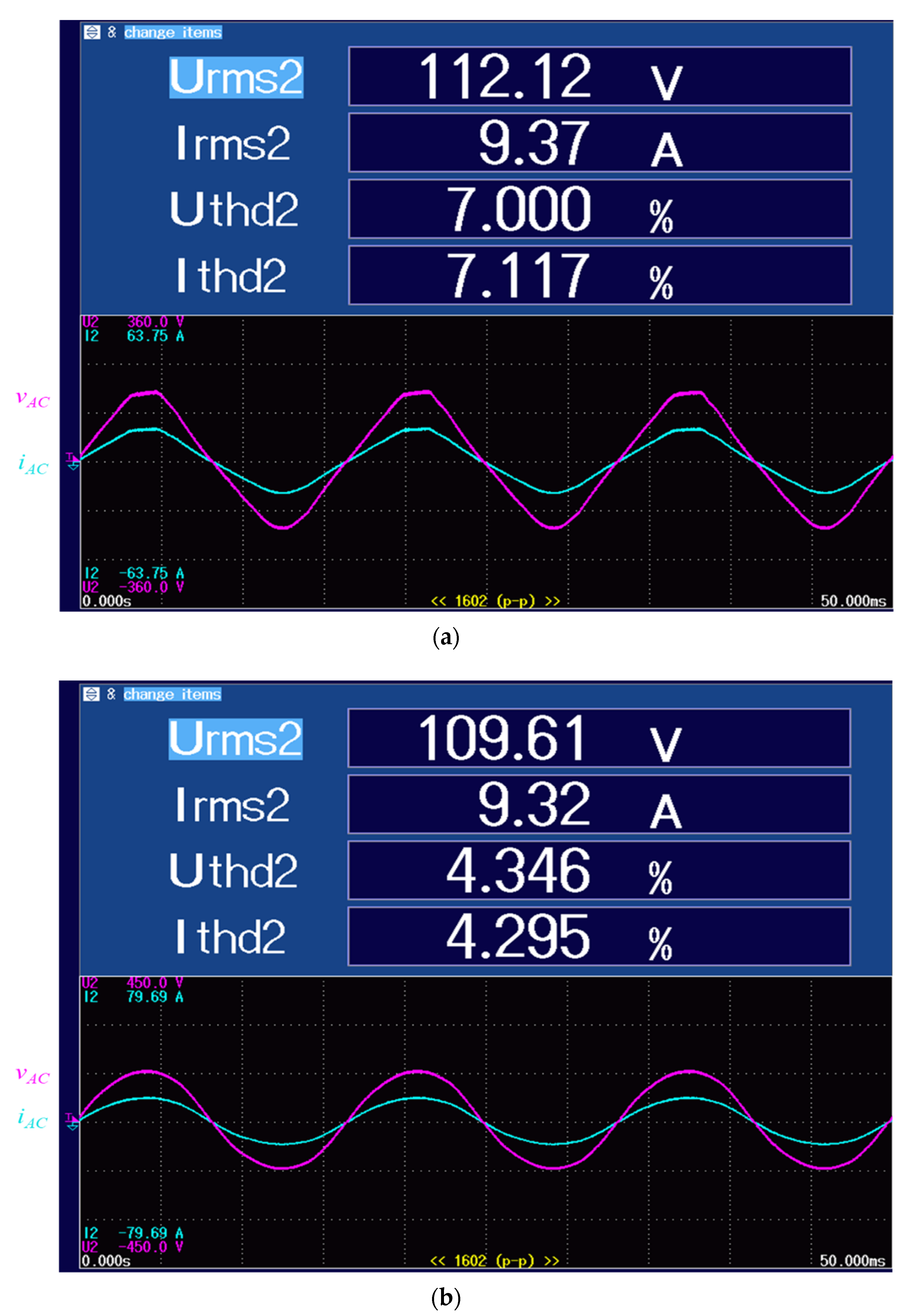
In addition, this study also analyzed the THD of the AC voltage output with simulations; the AC voltage output was the voltage difference between two capacitors and the voltage of the capacitors changed along with the switching frequency. Therefore, the THD was also affected by the switching frequency and the equivalent series resistance of the inductors L1 and L2. Figure 21, Figure 22 and Figure 23 show analyses of the simulation of the THD, where the THD of the traditional SPWM control was above 9%, while the THD of the modified SPWM was lower under 5%. The reason is related to the aforementioned phenomenon, which is shown in Figure 15, Figure 16, Figure 17, Figure 18, Figure 19 and Figure 20.
Finally, the actual experiments were implemented with the hardware shown in Figure 12. The THD analysis of the AC output voltage was performed with a Power Analyzer. The results are shown in Figure 24, Figure 25 and Figure 26, where the THD of the modified SPWM control was lower than the THD of the traditional SPWM control. The results are within the standard, for which there is a 5% limitation in IEEE Std 519-1992 and 8% in IEEE Std 519-2014 [19].
In summary, the SSDBI topology has been proposed and discussed in recent years. Voltage distortion will occur on the AC side when the traditional SPWM control is used with the SSDBI it is operated with high voltage gain [17]. This study certified this phenomenon with simulations and hardware experiments. To overcome this problem, this study analyzed the characteristics of the SSDBI and inferred an appropriate mathematical model of the duty according to the relationship between VAC and VDC (Equations (11) and (12)). Since the derived mathematical model of the duty modified the traditional SPWM control, the use of the modified SPWM control with the SSDBI improved the voltage distortion on the AC side and the THD. The SSDBI was tested under three different loads (25%, 50%, and 100%) to verify the theoretical predictions in both simulations and hardware experiments. After collating the above results, the improvement in the voltage distortion on the AC side can be observed in Figure 15, Figure 16, Figure 17, Figure 18, Figure 19 and Figure 20, and the comparison of the THD in the results of the simulations and hardware experiments can be observed in Table 3, where the THD in the simulations was close to that in the hardware experiments. The modified SPWM control had better performance than that of the traditional SPWM control.
5. Conclusions
When the traditional SPWM control is directly used in an SSDBI, waveform distortion and a high voltage peak will occur on the AC side. The problems increase the THD and the stress on the components of the inverter. Therefore, this study proposed a modified SPWM control for application to the SSDBI in order to overcome these problems in simulations and a hardware implementation. The results verified the performance of the SSDBI when the modified SPWM was applied; the distortion and the high voltage peak on the AC side were improved, and the modified SPWM control significantly decreased the inverter’s THD in both the simulations and the actual measurements. After the proposed modification, the proposed inverter can operate safely and can comply with the IEEE Std 519-1992 and IEEE Std 519-2014 standards.
Author Contributions
Conceptualization, Y.-L.L. and Y.-H.C.; methodology, K.-F.C.; software, Y.-H.C.; validation, Y.-L.L., K.-F.C. and Y.-H.C.; formal analysis, K.-J.P.; investigation, K.-F.C.; resources, K.-F.C.; data curation, Y.-L.L. and K.-J.P.; writing—original draft preparation, Y.-L.L.; writing—review and editing, C.-H.L.; visualization, Y.-L.L.; supervision, C.-H.L.; project administration, C.-H.L.; funding acquisition, K.-F.C. All authors have read and agreed to the published version of the manuscript.
Funding
The authors gratefully acknowledge the financial support of the Ministry of Science and Technology, Taiwan, R.O.C. under contract numbers MOST 110-2221-E-011-081, MOST 110-2622-E-011-004, and MOST 110-3116-F-011-002.
Institutional Review Board Statement
Not applicable.
Informed Consent Statement
Not applicable.
Data Availability Statement
Not applicable.
Acknowledgments
The authors sincerely appreciate the great support from the Taiwan Building Technology Center and from the Featured Areas Research Center Program within the framework of the Higher Education Sprout Project by the Ministry of Education in Taiwan.
Conflicts of Interest
The authors declare no conflict of interest.
References
- Liu, S.; Wang, X.; Liu, P.X. A Stochastic Stability Enhancement Method of Grid-Connected Distributed Energy Storage Systems. IEEE Trans. Smart Grid 2017, 8, 2062–2070. [Google Scholar] [CrossRef]
- Yeh, C.; Chen, C.; Lee, M.; Lai, J. A Hybrid Modulation Method for Single-Stage Soft-Switching inverter Based on Series Resonant Converter. IEEE Trans. Power Electron. 2020, 35, 5785–5796. [Google Scholar] [CrossRef]
- Lo, K.; Chen, Y.; Chang, Y. Bidirectional Single-Stage Grid-Connected inverter for a Battery Energy Storage System. IEEE Trans. Ind. Electron. 2017, 64, 4581–4590. [Google Scholar] [CrossRef]
- Li, X.; Li, Z.; Guo, L.; Zhu, J.; Wang, Y.; Wang, C. Enhanced Dynamic Stability Control for Low-Inertia Hybrid AC/DC Microgrid With Distributed Energy Storage Systems. IEEE Access 2019, 7, 91234–91242. [Google Scholar] [CrossRef]
- Nguyen, N.; Oruganti, S.K.; Na, K.; Bien, F. An Adaptive Backward Control Battery Equalization System for Serially Connected Lithium-Ion Battery Packs. IEEE Trans. Veh. Technol. 2014, 63, 3651–3660. [Google Scholar] [CrossRef]
- Wang, L.Y.; Wang, C.; Yin, G.; Lin, F.; Polis, M.P.; Zhang, C.; Jiang, J. Balanced Control Strategies for Interconnected Heterogeneous Battery Systems. IEEE Trans. Sustain. Energy 2016, 7, 189–199. [Google Scholar] [CrossRef]
- Omariba, Z.B.; Zhang, L.; Sun, D. Review of Battery Cell Balancing Methodologies for Optimizing Battery Pack Performance in Electric Vehicles. IEEE Access 2019, 7, 129335–129352. [Google Scholar] [CrossRef]
- Ding, G.; Gao, F.; Tian, H.; Ma, C.; Chen, M.; He, G.; Liu, Y. Adaptive DC-Link Voltage Control of Two-Stage Photovoltaic inverter During Low Voltage Ride-Through Operation. IEEE Trans. Power Electron. 2016, 31, 4182–4194. [Google Scholar] [CrossRef]
- Zhang, L.; Jiang, F.; Xu, D.; Sun, K.; Hao, Y.; Zhang, T. Two-Stage Transformerless Dual-Buck PV Grid-Connected inverters with High Efficiency. Chin. J. Electr. Eng. 2018, 4, 36–42. [Google Scholar]
- Thang, T.V.; Thao, N.M.; Jang, J.; Park, J. Analysis and Design of Grid-Connected Photovoltaic Systems With Multiple-Integrated Converters and a Pseudo-DC-Link inverter. IEEE Trans. Ind. Electron. 2014, 61, 3377–3386. [Google Scholar] [CrossRef]
- Abeywardana, D.B.W.; Hredzak, B.; Agelidis, V.G. A Rule-Based Controller to Mitigate DC-Side Second-Order Harmonic Current in a Single-Phase Boost inverter. IEEE Trans. Power Electron. 2016, 31, 1665–1679. [Google Scholar] [CrossRef]
- Huang, S.; Tang, F.; Xin, Z.; Xiao, Q.; Loh, P.C. Grid-Current Control of a Differential Boost inverter With Hidden LCL Filters. IEEE Trans. Power Electron. 2019, 34, 889–903. [Google Scholar] [CrossRef]
- Abeywardana, D.B.W.; Hredzak, B.; Agelidis, V.G. An Input Current Feedback Method to Mitigate the DC-Side Low-Frequency Ripple Current in a Single-Phase Boost inverter. IEEE Trans. Power Electron. 2016, 31, 4594–4603. [Google Scholar] [CrossRef]
- Chen, W.; Yang, C.; Lin, C.; Xu, M.; Chen, K. Voltage Modulation and Current Control of Boost inverters for Stand-Alone or Grid-Tied Operation. IEEE Trans. Power Electron. 2020, 35, 8726–8736. [Google Scholar] [CrossRef]
- Lopez-Caiza, D.; Flores-Bahamonde, F.; Kouro, S.; Santana, V.; Müller, N.; Chub, A. Sliding Mode Based Control of Dual Boost inverter for Grid Connection. Energies 2019, 12, 4241. [Google Scholar] [CrossRef] [Green Version]
- López-Santos, O.; García, G. Double Sliding-Surface Multiloop Control Reducing Semiconductor Voltage Stress on the Boost inverter. Appl. Sci. 2020, 10, 4912. [Google Scholar] [CrossRef]
- Jha, K.; Mishra, S.; Joshi, A. High-Quality Sine Wave Generation Using a Differential Boost inverter at Higher Operating Frequency. IEEE Trans. Ind. Appl. 2015, 51, 373–384. [Google Scholar] [CrossRef]
- Mwinyiwiwa, B.; Wolanski, Z.; Ooi, B.T. Microprocessor-Implemented SPWM for Multiconverters with Phase-Shifted Triangle Carriers. IEEE Trans. Ind. Appl. 1998, 34, 487–494. [Google Scholar] [CrossRef]
- Langella, R.; Testa, A.; Alii, E. IEEE Recommended Practice and Requirements for Harmonic Control in Electric Power Systems; IEEE Std 519-2014 Revision IEEE Std 519-1992; IEEE: New York, NY, USA, 2014; pp. 1–29. [Google Scholar]
Figure 1.
A block diagram of a BESS with a battery charger.

Figure 2.
The traditional topology of a BESS.

Figure 3.
Pseudo DC-link topology of a BESS.

Figure 4.
The single-stage topology of a BESS.

Figure 5.
The schematic of the SSDBI.

Figure 6.
The analytical model of the SSDBI.

Figure 7.
The operation states of the inverter: (a) Mode 1; (b) Mode 2; (c) Mode 3; (d) Mode 4.

Figure 8.
The relationships among the control signal, duty ratio, and AC output vAC in buck inverters with traditional SPWM control.
Figure 8.
The relationships among the control signal, duty ratio, and AC output vAC in buck inverters with traditional SPWM control.

Figure 9.
vAC waveform generated by the proposed inverter with SPWM control.

Figure 10.
A comparison between the traditional SPWM control and the modified SPWM control: (a) Vcontrol and (b) vAC.
Figure 10.
A comparison between the traditional SPWM control and the modified SPWM control: (a) Vcontrol and (b) vAC.

Figure 11.
System connections of the SSDBI.

Figure 12.
The laboratory setup of the test platform.

Figure 13.
Comparison of Vcontrol between the traditional SPWM and modified SPWM controls.

Figure 14.
The circuit diagram of the proposed inverter in the simulation.

Figure 15.
The simulation results (250 W) of the voltage and current output waveforms when using (a) the traditional SPWM control and (b) modified SPWM control.
Figure 15.
The simulation results (250 W) of the voltage and current output waveforms when using (a) the traditional SPWM control and (b) modified SPWM control.

Figure 16.
The simulation results (500 W) of the voltage and current output waveforms when using (a) the traditional SPWM control and (b) modified SPWM control.
Figure 16.
The simulation results (500 W) of the voltage and current output waveforms when using (a) the traditional SPWM control and (b) modified SPWM control.

Figure 17.
The simulation results (1 kW) of the voltage and current output waveforms when using (a) the traditional SPWM control and (b) modified SPWM control.
Figure 17.
The simulation results (1 kW) of the voltage and current output waveforms when using (a) the traditional SPWM control and (b) modified SPWM control.

Figure 18.
The measured results (250 W) of the voltage and current output waveforms when using (a) the traditional SPWM control and (b) modified SPWM control.
Figure 18.
The measured results (250 W) of the voltage and current output waveforms when using (a) the traditional SPWM control and (b) modified SPWM control.

Figure 19.
The measured results (500 W) of the voltage and current output waveforms when using (a) the traditional SPWM control and (b) modified SPWM control.
Figure 19.
The measured results (500 W) of the voltage and current output waveforms when using (a) the traditional SPWM control and (b) modified SPWM control.

Figure 20.
The measured results (1 kW) of the voltage and current output waveforms when using (a) the traditional SPWM control and (b) modified SPWM control.
Figure 20.
The measured results (1 kW) of the voltage and current output waveforms when using (a) the traditional SPWM control and (b) modified SPWM control.

Figure 21.
THD analysis of the simulation (250 W) when using (a) the traditional SPWM control and (b) modified SPWM control.
Figure 21.
THD analysis of the simulation (250 W) when using (a) the traditional SPWM control and (b) modified SPWM control.

Figure 22.
THD analysis of the simulation (500 W) when using (a) the traditional SPWM control and (b) modified SPWM control.
Figure 22.
THD analysis of the simulation (500 W) when using (a) the traditional SPWM control and (b) modified SPWM control.

Figure 23.
THD analysis of the simulation (1 kW) when using (a) the traditional SPWM control and (b) modified SPWM control.
Figure 23.
THD analysis of the simulation (1 kW) when using (a) the traditional SPWM control and (b) modified SPWM control.

Figure 24.
THD analysis in hardware experiments (250 W) when using (a) the traditional SPWM control and (b) modified SPWM control.
Figure 24.
THD analysis in hardware experiments (250 W) when using (a) the traditional SPWM control and (b) modified SPWM control.

Figure 25.
THD analysis in hardware experiments (500 W) when using (a) the traditional SPWM control and (b) modified SPWM control.
Figure 25.
THD analysis in hardware experiments (500 W) when using (a) the traditional SPWM control and (b) modified SPWM control.

Figure 26.
THD analysis in hardware experiments (1 kW) when using (a) the traditional SPWM control and (b) modified SPWM control.
Figure 26.
THD analysis in hardware experiments (1 kW) when using (a) the traditional SPWM control and (b) modified SPWM control.


Table 1.
The operation modes of Converter 1 and Converter 2.
| vAC | Mode | Status of Switch | Status of Converter |
|---|---|---|---|
| >0 | Mode 1 [t0~t1] | S1, S3 on S2, S4 off | |
| Mode 2 [t1~t2] | S2, S4 on S1, S3 off | ||
| <0 | Mode 3 [t2~t3] | S2, S4 on S1, S3 off | Converter 2: Boost (Charge C2) |
| Mode 4 [t3~t4] | S1, S3 on S2, S4 off | Converter 2: Boost (Charge C2) |
Table 2.
Specification of the proposed BESS.
| Item | Value |
|---|---|
| Battery module (voltage range) | 33.6–58.4 Vdc |
| Battery module (voltage rated) | 52.8 Vdc |
| AC output voltage | 110 Vrms |
| Power | 1000 W |
| Switching frequency | 21.6 kHz |
| Inductor | 120 μH, 120 μH |
| ESR of Inductor | 0.2 Ω, 0.2 Ω |
| Capacitor | 12 μF, 12 μF |
| ESR of Capacitor | 0.02 Ω, 0.02 Ω |
Table 3.
Comparison of the THD in the results of the simulations and hardware experiments.
| Results | THD | ||
|---|---|---|---|
| 250 W | 500 W | 1000 W | |
| Simulation (traditional) | 9.12% | 8.64% | 6.83% |
| Simulation (modified) | 3.47% | 3.33% | 4.24% |
| Hardware experiment (traditional) | 9.20% | 8.78% | 7.00% |
| Hardware experiment (modified) | 3.66% | 3.50% | 4.29% |
Publisher’s Note: MDPI stays neutral with regard to jurisdictional claims in published maps and institutional affiliations. |
© 2021 by the authors. Licensee MDPI, Basel, Switzerland. This article is an open access article distributed under the terms and conditions of the Creative Commons Attribution (CC BY) license (https://creativecommons.org/licenses/by/4.0/).
Share and Cite
MDPI and ACS Style
Lee, Y.-L.; Chen, K.-F.; Pai, K.-J.; Lin, C.-H.; Cheng, Y.-H. Modified SPWM Control for a Single-Stage Differential Boost Inverter Applied in a BESS. Processes 2021, 9, 1861. https://0-doi-org.brum.beds.ac.uk/10.3390/pr9111861
AMA Style
Lee Y-L, Chen K-F, Pai K-J, Lin C-H, Cheng Y-H. Modified SPWM Control for a Single-Stage Differential Boost Inverter Applied in a BESS. Processes. 2021; 9(11):1861. https://0-doi-org.brum.beds.ac.uk/10.3390/pr9111861
Chicago/Turabian StyleLee, Yu-Lin, Kun-Feng Chen, Kai-Jun Pai, Chang-Hua Lin, and Yuan-Hong Cheng. 2021. "Modified SPWM Control for a Single-Stage Differential Boost Inverter Applied in a BESS" Processes 9, no. 11: 1861. https://0-doi-org.brum.beds.ac.uk/10.3390/pr9111861
Note that from the first issue of 2016, this journal uses article numbers instead of page numbers. See further details here.