Stacked Chip-Based Terahertz Metamaterials and Their Application
by
Han Wang
1, 
Zhigang Wang
1,
Bo Yan
1,
Xinyu Li
2,
Chenrui Zhang
2,
Huiqi Jiang
2,
Minghui Deng
2,
Lesiqi Yin
2 and
Cheng Gong
2,* 1
School of Electronic Science and Engineering, University of Electronic Science and Technology of China, Chengdu 611731, China
2
Tianjin Key Laboratory of Micro-Scale Optical Information Science and Technology, Institute of Modern Optics, Nankai University, Tianjin 300350, China
*
Author to whom correspondence should be addressed.
Photonics 2023, 10(11), 1226; https://0-doi-org.brum.beds.ac.uk/10.3390/photonics10111226
Submission received: 24 September 2023
/
Revised: 26 October 2023
/
Accepted: 30 October 2023
/
Published: 1 November 2023
(This article belongs to the Special Issue Terahertz Transmission and Imaging)
Abstract
:A terahertz (THz) metamaterial design mechanism based on a stacked chip is proposed. Unlike the traditional sandwich-type metamaterial design mechanism based on the “resonant layer–dielectric layer–ground layer” structure, it adopts a stacked design of upper and lower metamaterial chips to achieve a new structure based on the “dielectric layer–resonant layer–air layer–ground layer” structure. This could break through the thickness limitations and construct an ultra-thin metamaterial upper chip. To verify the effectiveness of this method, we applied it to the field of THz perfect absorbers. We designed, simulated, and prepared a terahertz stacked chip-based perfect absorber with an upper-chip thickness less than 1/800 of the wavelength. Then, a reflective spectroscopy system based on a vector network analyzer is built to test the absorption performance. The measured results show that it has an absorptivity of 98.4% at 0.222 THz, which is in good agreement with simulations.
1. Introduction
Terahertz (THz) waves are the electromagnetic waves with a frequency of 0.1 THz~10 THz, also known as the “terahertz gap” in the electromagnetic spectrum. It is considered to be the core frequency band of the next generation of high-frequency electronics and communication technology, but there is a lack of materials in nature that can directly modulate terahertz waves. Fortunately, owing to the emergence of metamaterials, it will be possible to overcome this problem [1,2,3,4,5]. Metamaterials, artificial micro-structure periodic arrays, could provide unprecedented abilities to manipulate electromagnetic waves by changing the periodic units’ geometric structures and dimensions. Many outstanding achievements or applications based on metamaterials have been proposed, including artificial magnetic material [6], negative refraction [7], the super-lens [8], the cloak [9], the perfect absorber [10,11], and the modulator [12,13]. Currently, the thickness of most metamaterial absorbers is typically between a fraction and a hundredth of the operating wavelength (≥1/100 wavelength) [14,15,16,17,18,19,20,21,22]. Although it is already very thin, researchers have been pursuing ultra-thin thickness in some special THz applications, such as sensing [23,24], imaging lenses [25,26], and absorption [27,28]. This is because they can achieve a higher sensitivity, smaller volume, and higher absorption performance. However, the traditional THz metamaterials are based on the sandwich structure mechanism of the “resonant layer–dielectric layer–ground layer” structure [29,30,31,32], or the full dielectric structure mechanism [33,34,35,36]. The above mechanisms require the design and processing of the electric resonance structure, magnetic resonance structure, and support structure of metamaterials as a whole, fundamentally limiting the further reduction in the thickness of the core structure of metamaterial components.
Therefore, to solve this problem, we propose a terahertz metamaterial design mechanism based on a stacked chip. A structure based on the “dielectric layer–resonant layer–air layer–ground layer” structure has been formed by designing the upper and lower metamaterial chips separately and then stacking them. With the help of the “air layer”, the resonant layer and auxiliary support structure layer of the metamaterial have been separated, allowing for the breakthrough of thickness limitations and the construction of an ultra-thin metamaterial upper chip. In addition, to verify the effectiveness of this method, we applied it to the study of perfect absorbers. Through a literature research, it can be found that many terahertz metamaterial absorbers, in order to achieve excellent absorptivity (greater than 90%), typically have a thickness between 1/2 and 1/100 of the wavelength [17,18,19,20,21]. A further reduction in the thickness would result in a rapid decline in the absorption. To overcome this contradiction, we designed and prepared a terahertz perfect absorber based on a stacked chip, with an upper chip thickness less than 1/800 of the wavelength. Then, we build a reflective spectroscopy system based on a vector network analyzer to test the absorption performance. The measurement results indicate that the absorption rate can reach 98.4% at 0.222 THz under the condition of ultra-thin thickness.
2. Design and Principle
Figure 1 depicts the schematic diagram of the composition of stacked chip-based terahertz metamaterials, which designs the upper chip and the lower chip separately, and then stacks them together to form a stacked chip. The upper chip performs core functions and can be combined with other technologies to form sensors, imaging detectors, modulators, and so on. The lower chip implements the functions of auxiliary regulation and support substrate.
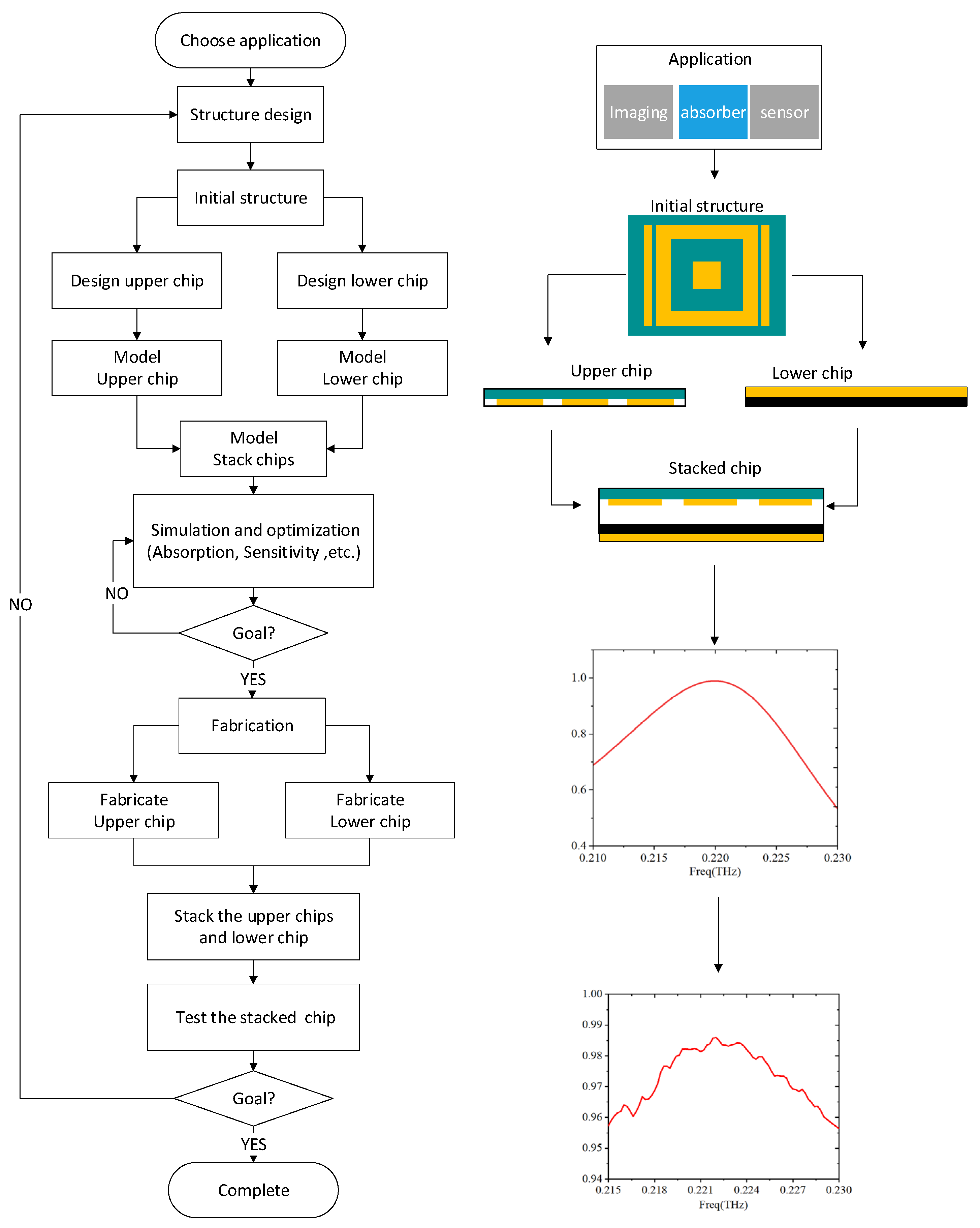
The design flow chart of the stacked chip-based THz metamaterials can be shown in Figure 2. The first thing to be determined is the specific application of the designed metamaterial chip, such as THz sensors, imaging lenses, absorbers, etc. Different applications correspond to different structures. Therefore, the second step is to select the initial material of the metamaterial chip and determine the initial unit structure based on the specific application and technical specifications. It should be noted that the designed terahertz metamaterial chip is composed of a stack of upper and lower layers of chips, with the upper chip achieving core functions and the lower chip achieving auxiliary regulation functions. Therefore, the third step is to divide the structure, design the upper and lower chip structures separately, and model them in electromagnetic simulation software. It should be mentioned that an air cavity layer will be formed between the two chips. The fourth step is combining the upper and lower chips to establish an initial stacked terahertz metamaterial chip model.
After that, the initial model should be simulated and analyzed based on the application requirements. The structural and dimensional parameters are gradually optimized according to the simulation results. Then, determine whether the design indicators (such as absorption rate, sensitivity, etc.) are met. If the indicators are not met, return to continue modifying and optimizing the relevant parameters. If the indicators are met, proceed to the fifth step of “fabrication”. In this step, semiconductor-based processes (such as coating, lithography, and etching) are typically used to fabricate the upper chip and the lower chip separately. Then, the chips are stacked. The sixth step is to test the performance parameters of the stacked chip using a THz-TDS (terahertz-time domain spectrometer) or high-frequency vector network analyzer. If the test results do not meet the design specifications, it is necessary to redesign and optimize the structure, re-model and simulate, repeat the optimization steps, and reprocess the test chip until the design specifications are met. The left side in Figure 2 is a flow chart of the entire design process, and the right side in Figure 2 is a schematic diagram of the key design process.
In order to further explain the design ideas of the stacked metamaterial chip, we take the design of classic square-ring metamaterial as an example, and, respectively, give the model schematic diagrams based on the traditional sandwich design idea and the stacked chip-based design idea, as shown in Figure 3. Among them, Figure 3a is a side-view schematic of a metamaterial chip based on the traditional sandwich design concept, which is composed of a metal resonant layer, a dielectric layer, and a metal ground layer. The entire chip is an inseparable whole. Figure 3b depicts a side-view diagram of the metamaterial chip based on the design idea of the stacked chip. It can be seen that the upper chip and the lower chip are stacked, the upper chip is composed of a dielectric layer and a metal resonance layer, and the lower chip is composed of a metal layer and an air layer. The entire metamaterial chip adopts a separate design. Compared with the traditional structure, the dielectric layer and the metal resonant layer of the new structure are placed in reverse position. In addition, the upper chip is used as the core structure, and the performance parameters of the chip can be adjusted by designing the upper chip. Besides, some electromagnetic parameters, such as the operating frequency and resonance intensity, can also be adjusted by designing gaps in the air layer.
Figure 3c depicts the three-dimensional schematic of the metamaterial chip based on the traditional sandwich design concept. It can be seen that the thickness of this type of metamaterial structure is limited by the dielectric layer between the resonant layer and the metal ground layer, and it is difficult to further reduce the thickness without ensuring the same performance. In situations where ultra-thin thickness (such as highly sensitive sensors, ultra-thin imaging lenses, and ultra-thin absorbers) is required, it will be difficult to achieve optimal performance. Figure 3d shows the three-dimensional diagram of the metamaterial chip based on the design idea of the stacked chip. It can be seen that by stacking the upper and lower chips, a new structure based on the “dielectric layer–resonant layer–air layer–ground layer” structure is achieved. The upper chip (dielectric layer and resonant layer) performs the core functions, while the lower chip (air layer and ground layer) performs auxiliary adjustment functions. Based on this design, the thickness of the upper chip can be reduced to the greatest extent under the premise of ensuring the optimal performance of the metamaterial chip.
The above design method may increase the design complexity and time, but it also has unique advantages, which are as follows:
- (1)
- The upper chip and the lower chip are designed separately, making the design more flexible;
- (2)
- The stacking of the upper and lower chips can make the upper chip very thin (<1/800 wavelength), achieving some characteristics that, with traditional terahertz metamaterials, are difficult to achieve.
For example, it can be used to construct ultra-thin upper-chip structures, and then combined with MEMS (micro-electro-mechanical systems) technology to construct terahertz sensors, achieving a higher sensitivity. To verify this viewpoint, we compared it with traditional metamaterial structures. Figure 4a shows a schematic diagram of the stacked metamaterial, while Figure 4b is a schematic diagram of a metamaterial using a traditional sandwich design structure. Although both schemes can achieve the perfect absorption of terahertz, due to the fact that the thickness of the upper chip of stacked metamaterials is only 1/10 of that of traditional metamaterials, the temperature rise is faster after absorbing electromagnetic waves of the same energy (1 mW). We simulated the time-temperature curves of two structures under terahertz radiation using the EM thermal coupling module of CST STUDIO SUITE. The specific simulation method is as follows: Firstly, electromagnetic simulations are performed to calculate the heat loss distributions. During the simulation process, the boundary conditions are set to unit cell in the x and y directions and open (add space) in the z direction. The tetrahedral meshing and frequency domain solver based on finite element method are used for simulation. Secondly, after obtaining the heat loss distribution, thermal simulation is carried out. During the simulation process, the background material is set to air and the background temperature is 293.15 k. The boundary conditions are set to open in the x and y directions and open (add space) in the z direction. The tetrahedral meshing and thermal transient solver are used for the simulation to obtain the temperature distributions.
As shown in Figure 4c, the upper chip of the stacked metamaterial can achieve a higher temperature rise in a shorter time. The higher the temperature rise, the greater the degree of mechanical deformation. If we add pressure-sensitive materials in the area with the greatest deformation and read the voltage changes through a voltage probe, we can construct a highly sensitive terahertz detector, as shown in Figure 4d. In addition, the stacked metamaterial design will increase the repetition frequency of the detector. The main reasons are as follows: (1) After the metamaterial chip heats up, there are two main ways to cool down; one is to transfer heat through air, and the other is to transfer heat through the chip’s own material. Because the metal resonant layer is a series of discontinuous periodic unit structures, its heat transfer must be carried out through the air and dielectric layers, so the main consideration is the heat transfer of air, the dielectric layer, and the metal ground. It is known that the thermal conductivity of air is about 0.026 W/m∙K, the thermal conductivity of the dielectric layer’s silicon nitride material is about 140 W/m∙K, and the thermal conductivity of gold is about 317 W/m∙K, so the thermal conductivity of air is almost negligible, and the chips are mainly located in the dielectric layer and metal ground for heat conduction and cooling. (2) The thermal resistance of traditional metamaterials and stacked metamaterials can be calculated for quantitative analysis. As is well known, thermal resistance is the ability of a material to hinder heat conduction. The larger the thermal resistance of a thermal conductive material, the stronger its resistance to heat conduction and the less likely it is to cool down. On the contrary, the smaller the thermal resistance, the easier it is to cool down. The calculation formula for thermal resistance R is as follows:
Here, d is the thickness of the material, k represents the thermal conductivity of the material, and S is the cross-sectional area in the direction of the heat flow rate. This is because stacked metamaterials consist of an upper chip and a lower chip, and the upper chip has only a very thin dielectric layer on it. Therefore, the main method of heat conduction and cooling is achieved through the dielectric layer. Assuming that the thickness of the upper chip dielectric layer is about 1/10 of that of the traditional metamaterials, the thermal resistance of stacked metamaterials will be less than 1/10 of the thermal resistance of traditional metamaterials. Therefore, heat conduction is faster and cooling is faster, which effectively improves the repetition frequency of the detector. In summary, the design mechanism based on stacked chip breaks through design limitations and minimizes the thickness of the upper chip, laying the foundation for the research of ultra-thin and high-performance metamaterial chips.
3. Application for Perfect Absorption
To demonstrate the effectiveness of the metamaterial design mechanism, we apply it to the terahertz perfect absorption field. As is well known, the thickness and absorption have always been two conflicting key parameters in designing a high-performance absorber. However, in the case of perfect absorption, the thinner the thickness, the more advantageous it is to improve the response performance and reduce the power consumption of terahertz components. Therefore, we will design an ultra-thin (upper chip) terahertz perfect absorption chip based on the stacked structure.
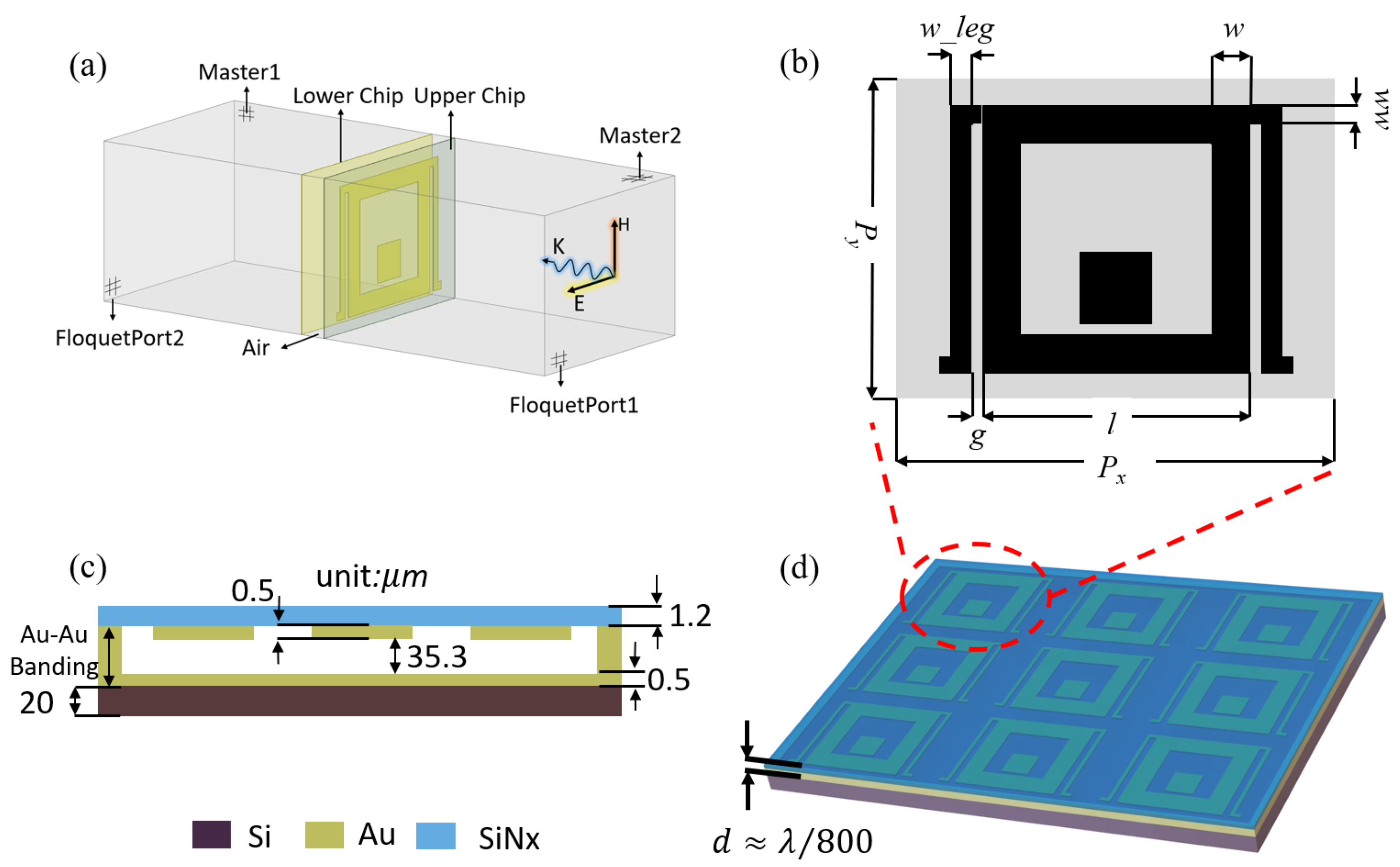
According to the proposed design process, we first determine the application field as the perfect absorption of terahertz waves, and then determine the initial structure of the metamaterial periodic unit. This structure can be based on classical resonant structures and gradually expanded from simple to complex. In this article, the initial structure chosen is a classical square ring combined with a pair of resonant arms. The upper chip uses SiNx as the dielectric layer and gold as the resonance layer, which plays the core absorption role. When the terahertz wave illuminates the upper chip, the resonant layer generates resonance, and performs the efficient absorption of terahertz energy under the joint action of the dielectric layer. The lower chip serves as an auxiliary regulation chip, using gold as the ground layer and leaving an air layer in the middle. By adjusting the size of the air layer, the absorption rate and frequency of the absorption chip can be further adjusted. Then, establish a model in the electromagnetic simulation software HFSS 19.0 and conduct the simulation. Based on the simulation results, the chip is iteratively optimized until it meets the required indicators. Figure 5a depicts the simulation model. Figure 5b shows the structure of a unit of the terahertz metamaterial absorption chip, with a size of 315 μm × 425 μm. Figure 5c shows the side view of the chip. It can be seen that the upper chip uses 1.2 μm SiNx as the dielectric layer and 0.5 μm gold as the resonance layer, so the thickness of the upper chip is only 1.7 μm (about 1/800 of the wavelength). The lower chip uses 0.5 μm gold as the metal ground layer and silicon as the substrate. The upper and lower chips are combined by gold–gold bonding to complete the stack. The three-dimensional diagram of the bonded chip is shown in Figure 5d.
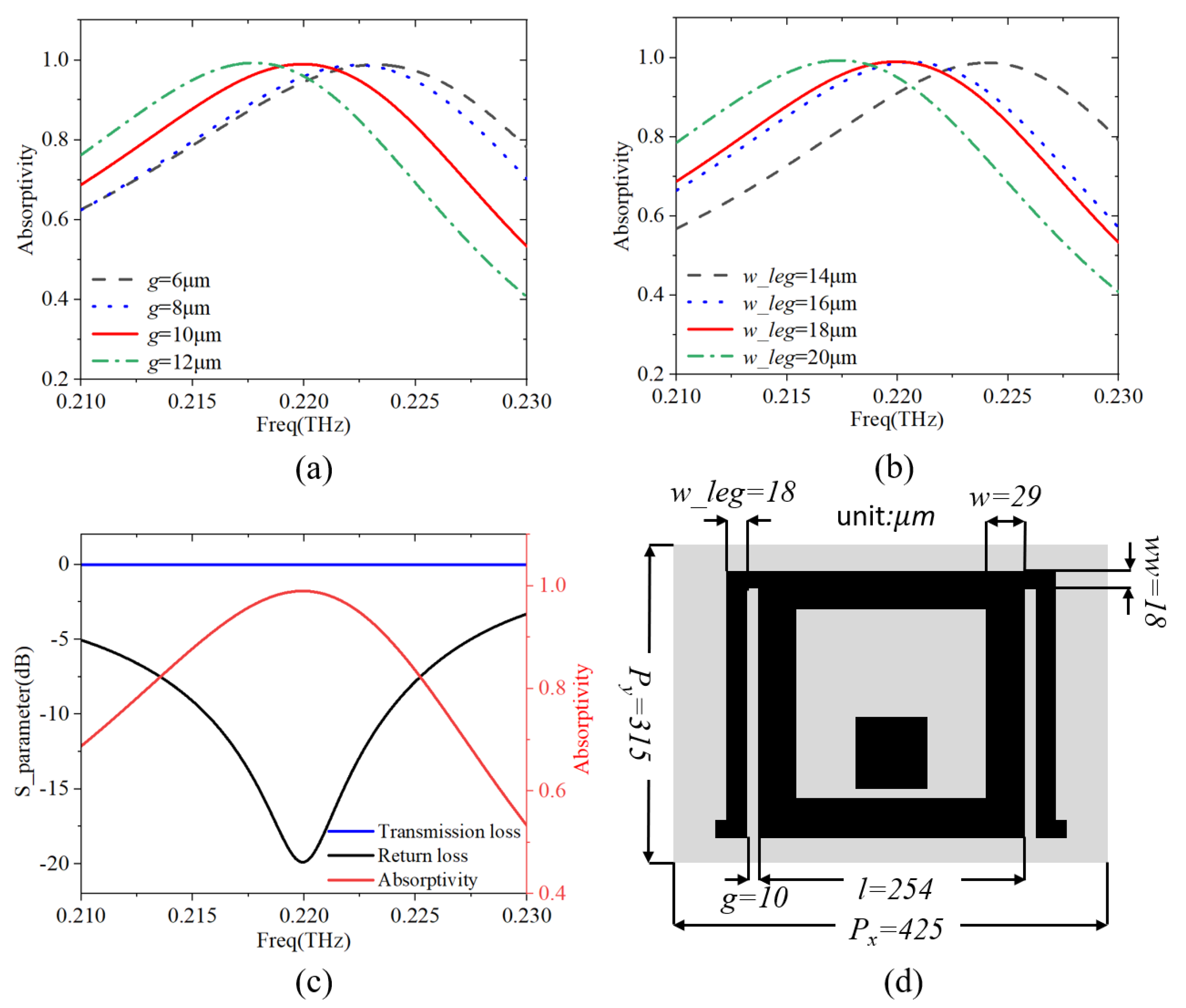
Next, it is necessary to further optimize and analyze the size parameters of the established model. As shown in Figure 6, the gap g between the ring and the resonant arms and the width w_leg of the resonant arms were simulated by the parametric scanning of the absorption spectrum. The influence of these two parameters on the performance of the absorber was analyzed, and the optimal absorption spectrum and optimized overall structure size were obtained according to the simulation results.
Figure 6a depicts the influence of the gap g between the resonant square ring and the resonant arm on the absorption frequency of the metamaterial absorption chip. It can be seen from the simulation results that when the gap increases from 6 μm to 12 μm, the absorption frequency of the stacked metamaterial absorption chip moves from 0.218 THz to 0.224 THz. Figure 6b shows the effect of the resonant arm width w_leg on the absorption frequency of the metamaterial absorption chip, where the absorption frequency of the metamaterial absorption chip moves from 0.225 THz to 0.216 THz when the width increases from 14 μm to 20 μm. Finally, we selected the desired 0.220 THz as the optimal absorption frequency point, and the S parameters and absorption curve obtained after parameter optimization are shown in Figure 6c. The absorptivity exceeds 99% at 0.22 THz and exceeds 80% at 0.21–0.23 THz. The specific dimensions of the optimized structural unit are shown in Figure 6d. It could be concluded from the simulation results that the THz metamaterial absorber designed based on the stacked chip scheme has nearly 100% absorption performance when the thickness of upper chip is less than 1/800 of the wavelength.
The equivalent circuit model of the metamaterial can be used to analyze the absorption mechanism of the chip. The absorber is composed of a stacked upper chip and lower chip, so it can be equivalent to two resonant circuits, as shown in Figure 7a,b. Among them, Figure 7a represents the resonant circuit of the upper chip. Its metal square ring and double arms structure generates equivalent capacitance C1, C2; equivalent inductance L1, L2; and equivalent resistance R1, R2. Figure 7b shows the resonant circuit formed by stacking the upper and lower chips. The resonant structure of the upper chip and the metal ground of the lower chip can be equivalent to capacitance C3 and C4. The current generated by the resonant structure of the upper chip is reversed from the induced current generated by the metal ground, resulting in an equivalent inductance L3. When the terahertz wave irradiates the metamaterial chip, it will cause strong resonance at the resonant frequency point and generate strong resonant currents. They are mainly dissipated in equivalent resistors R1 and R2, converting energy into heat, so electromagnetic waves can be absorbed perfectly.
We simulated the electric field distribution of the upper chip and found that the resonant electric field is mainly distributed between the square ring and the resonant arm, consistent with the equivalent circuit, as shown in Figure 7c. Meanwhile, by simulating the electric field distributions of the lower chip and the stacked chip, it can be seen that the reverse induced electric field generated by the metal ground of the lower chip is consistent with the position of the upper chip, as shown in Figure 7d,e. At the same time, the resonant electric field is mainly concentrated near the double resonant arms of the upper chip, and the resonant electric field of the upper chip is obviously stronger than that of the lower chip. Therefore, the upper chip can perform the core function, and the lower chip can perform the auxiliary regulation.
4. Test and Analysis
According to the proposed design process, the next step is to prepare and test the designed metamaterial absorption chip, and then analyze whether the test results meet the design indicators.
Figure 8 presents the fabrication process of the stacked metamaterial absorber, including the upper and lower chip processes. In the upper chip process, a silicon wafer is selected for the double-sided polishing firstly as shown in Figure 8a. The polishing technology is used to ensure the uniformity of the back ICP silicon etching. Then, the double-sided SiNx deposition is performed on the upper chip. Thirdly, the upper chip is photolithographed and etched to form a patterned silicon nitride thin film framework structure. Fourthly, the upper chip is photolithographed, coated with gold film, and lifted off to form a patterned metal structure. Fifthly, the dry etching (ICP) technology was used to etch the silicon substrate of the upper chip. Then, the silicon substrate of the upper chip is further etched using wet etching technology until it is completely removed.
Meanwhile, as shown in Figure 8b, a silicon wafer is selected for double-sided polishing. Then, the lower chip is photolithographed and etched to form a cavity with a depth of 35.8 µm. Next, the lower chip is coated to form a metal film plate with a thickness of 500 nm. Finally, the upper and lower chips are bonded together using bonding technology to form a stacked metamaterial chip as shown in Figure 8c. Besides, we give a comparison between this processing method and the traditional metamaterial processing method. It can be seen that although the process of traditional metamaterial absorbers is simpler and faster, the proposed stacked metamaterials can achieve ultra-thin chip thickness.
We compare the advantages and disadvantages of the processing of laminated metamaterials with those of conventional metamaterial processing methods, as shown in Table 1.
The prepared chip is shown in Figure 9, where Figure 9a is the photo of the absorption chip, and Figure 9b depicts the micrograph of the 3 × 3 units taken with a microscope. The overall size of the chip is 2.2 cm × 2.8 cm, with 50 × 50 = 2500 absorber unit cells.
Next, test the spectral characteristics of the processed chip and obtain the absorption performance through the results. What need to be tested are the reflection spectrum and the transmission spectrum, and then the calculation formula for the absorption spectrum can be expressed as
here, R(ω) stands for reflection, T(ω) is the transmission. It should be mentioned that S11 and S21 are the S parameters of metamaterial chips, representing the reflection and transmission performance of the chip, respectively. Among them, R(ω)=|S11|2 and T(ω)= |S21|2. Since the lower chip of the designed stacked metamaterial terahertz absorber contains a metal ground layer, the terahertz wave cannot penetrate, so the transmittance T(ω) = 0. After simplification, the calculation formula for the absorption spectrum is
After that, we built a reflective spectroscopy system based on a vector network analyzer to test the S parameters of the processed absorption chip. Figure 10a shows the block diagram of the test of the reflectance spectroscopy system. Port 1 of the vector network analyzer is connected to a collimated antenna, and the emitted terahertz wave is focused by a lens and then radiated to a chip or reflector plate, where a symmetrical focusing lens at the other end receives and focuses the reflected terahertz wave, which is then transmitted by the collimated antenna to port 2 of the vector network analyzer.
In order to accurately measure the S parameter, two steps are needed. The first step is to measure an object with near 100% reflectivity (gold plane reflector) as calibration to obtain the S-parameter Sca. The second step is to keep the test system unchanged, replace the gold reflector with the metamaterial chip as a sample for data measurement, and obtain Ssa. Considering the loss of the environment (e.g., air), the two S parameters need to subtract, and the final S parameter is S = Ssa − Sca. Finally, the absorption spectrum can be calculated by Formula 2, and the obtained actual absorption spectrum of the metamaterial chip is shown in Figure 10b.
It can be seen from Figure 10b that the peak optimal absorption frequency of the chip is 0.222 THz, and the measured absorption at this frequency is 98.4%, which is close to perfect absorption. The absorptivity exceeds 95% in the entire frequency band 0.215–0.230 THz. This experimental result shows a bias of 2 GHz in the optimal absorption frequency compared to the simulation result, mainly because there are inaccuracies in the processing, and the structural dimensions of the metamaterial absorber are not exactly the same as the simulation result. The actual processed sample size is slightly smaller than the simulation size, resulting in a decrease in the equivalent capacitance and inductance of the resonant structure of the upper chip in the electromagnetic field, thus shifting the resonant frequency towards high frequencies. Despite these objective errors, they do not affect the practical application of the chip. From the experimental results, we still achieved the goal of maintaining high absorption at a specific frequency with an upper chip’s thickness of only about 1/800 of the wavelength.
In addition, we surveyed the recent literature on ultra-thin THz metamaterial absorbers. Then, five representative papers were selected and compared with our work, as shown in Table 2. It can be concluded that the stacked chip metamaterial absorber has high absorptivity and the thinnest functional layer (upper chip) thickness.
5. Conclusions
In summary, a novel terahertz metamaterials design mechanism based on a stacked chip is demonstrated. By taking advantage of the design that separates the upper and lower chips to achieve a new structure based on the “dielectric layer–resonant layer–air layer–ground layer” structure, the upper chip’s thickness of the metamaterial can be reduced to less than 1/800 of the wavelength. To verify the proposed design, we have applied it to the field of THz perfect absorption. We designed, fabricated, and demonstrated an ultra-thin THz metamaterial perfect absorber whose optimal absorption frequency is 0.22 THz. Then, a reflective spectroscopy measurement system based on the vector network analyzer was built to test the absorption of the sample. The tested results agreed with the simulation results. Considering the unparalleled ultra-thin thickness and excellent performance, we believe that the THz metamaterials and its design mechanism based on a stacked chip can serve as a promising platform to develop advanced devices for a wider range of THz applications, especially in fields such as THz high-sensitivity sensing, compact meta-lenses, and perfect absorption.
Author Contributions
Conceptualization, C.G.; methodology, C.G.; software, C.G., H.W. and Z.W.; validation, H.W. and Z.W.; formal analysis, H.W., Z.W. and B.Y.; investigation, H.W. and Z.W.; resources, H.W. and Z.W.; data curation, H.W. and Z.W.; writing—original draft preparation, H.W. and Z.W.; writing—review and editing, C.G. and Z.W.; visualization, X.L., C.Z., H.J., M.D. and L.Y.; supervision, C.G.; project administration, C.G., B.Y. and Z.W. All authors have read and agreed to the published version of the manuscript.
Funding
This research received no external funding.
Institutional Review Board Statement
Not applicable.
Informed Consent Statement
Not applicable.
Data Availability Statement
The data underlying the results presented in this paper are not publicly available at this time but may be obtained from the authors upon reasonable request.
Acknowledgments
We would like to extend our sincere gratitude towards Nanjing Institute of Astronomical Optics & Technology, National Astronomical Observatories (CAS), and the 55th Research Institute of China Electronics Technology Corporation (CETC) for their support.
Conflicts of Interest
All The authors declare no conflict of interest.
References
- Xu, R.; Xu, X.; Yang, B.-R.; Gui, X.; Qin, Z.; Lin, Y.-S. Actively logical modulation of MEMS-based terahertz metamaterial. Photon. Res. 2021, 9, 1409–1415. [Google Scholar] [CrossRef]
- Ozpinar, H.; Aksimsek, S. Fractal interwoven resonator based penta-band metamaterial absorbers for THz sensing and imaging. Sci. Rep. 2022, 12, 1–10. [Google Scholar] [CrossRef] [PubMed]
- Mittleman, D. Metamaterials—A tunable terahertz response. Nat. Photonics 2008, 2, 267–268. [Google Scholar] [CrossRef]
- Chen, H.T.; Padilla, W.J.; Zide, J.M.O.; Gossard, A.C.; Taylor, A.J.; Averitt, R.D. Active terahertz metamaterial devices. Nature 2006, 444, 597–600. [Google Scholar] [CrossRef] [PubMed]
- Tao, H.; Landy, N.I.; Bingham, C.M.; Zhang, X.; Averitt, R.D.; Padilla, W.J. A metamaterial absorber for the terahertz regime: Design, fabrication and characterization. Opt. Express 2008, 16, 7181–7188. [Google Scholar] [CrossRef] [PubMed]
- Yen, T.J.; Padilla, W.J.; Fang, N.; Vier, D.C.; Smith, D.R.; Pendry, J.B.; Basov, D.N.; Zhang, X. Terahertz magnetic response from artificial materials. Science 2004, 303, 1494–1496. [Google Scholar] [CrossRef] [PubMed]
- Smith, D.R.; Pendry, J.B.; Wiltshire, M.C.K. Metamaterials and negative refractive index. Science 2004, 305, 788–792. [Google Scholar] [CrossRef] [PubMed]
- Zhang, X.; Liu, Z. Superlenses to overcome the diffraction limit. Nat. Mater. 2008, 7, 435–441. [Google Scholar] [CrossRef]
- Schurig, D.; Mock, J.J.; Justice, B.J.; Cummer, S.A.; Pendry, J.B.; Starr, A.F.; Smith, D.R. Metamaterial electromagnetic cloak at microwave frequencies. Science 2006, 314, 977–980. [Google Scholar] [CrossRef]
- Landy, N.I.; Sajuyigbe, S.; Mock, J.J.; Smith, M.D.R.; Padilla, W.J. Perfect metamaterial absorber. Phys. Rev. Lett. 2008, 100, 207402. [Google Scholar] [CrossRef]
- Watts, C.M.; Liu, X.; Padilla, W.J. Metamaterial electromagnetic wave absorbers. Adv. Mater. 2012, 24, OP98–OP120. [Google Scholar] [CrossRef] [PubMed]
- Badri, S.H.; Gilarlue, M.M.; SaeidNahaei, S.; Kim, J.S. Narrowband-to-broadband switchable and polarization-insensitive terahertz metasurface absorber enabled by phase-change material. J. Opt. 2022, 24, 025101. [Google Scholar] [CrossRef]
- Badri, S.H.; Soofi, H.; SaeidNahaei, S. Thermally reconfigurable extraordinary terahertz transmission using vanadium dioxide. J. Opt. Soc. Am. B 2022, 39, 1614–1621. [Google Scholar] [CrossRef]
- Hao, J.; Wang, J.; Liu, X.; Padilla, W.J.; Zhou, L.; Qiu, M. High performance optical absorber based on a plasmonic metamaterial. Appl. Phys. Lett. 2010, 96, 251104. [Google Scholar] [CrossRef]
- Li, M.; Xiao, S.; Bai, Y.Y.; Wang, B.Z. An Ultrathin and Broadband Radar Absorber Using Resistive FSS. IEEE Antennas Wirel. Propag. Lett. 2012, 11, 748–751. [Google Scholar]
- Maniotis, K.I.; Kliros, G.S. Design of an Ultra-Thin Bandwidth-Optimized Metamaterial Absorber for EMC Applications. In Proceedings of the 2015 23rd Telecommunications Forum Telfor (Telfor), Belgrade, Serbia, 24–26 November 2015; pp. 583–586. [Google Scholar]
- Gong, C.; Zhan, M.Z.; Yang, J.; Wang, Z.G.; Liu, H.T.; Zhao, Y.J.; Liu, W.W. Broadband terahertz metamaterial absorber based on sectional asymmetric structures. Sci. Rep. 2016, 6, srep32466. [Google Scholar] [CrossRef]
- Zhu, H.; Wang, K.; Liu, G.; Mou, J.; Wu, Y.; Zhang, Z.; Qiu, Y.; Wei, G. Metasurface absorber with ultra-thin thickness designed for a terahertz focal plane array detector. Opt. Express 2022, 30, 15939–15950. [Google Scholar] [CrossRef]
- Liu, Y.; Huang, R.; Ouyang, Z. Terahertz absorber with dynamically switchable dual-broadband based on a hybrid metamaterial with vanadium dioxide and graphene. Opt. Express 2021, 29, 20839–20850. [Google Scholar] [CrossRef]
- Wang, S.; Cai, C.; You, M.; Liu, F.; Wu, M.; Li, S.; Bao, H.; Kang, L.; Werner, D.H. Vanadium dioxide based broadband THz metamaterial absorbers with high tunability: Simulation study. Opt. Express 2019, 27, 19436–19447. [Google Scholar] [CrossRef]
- Alves, F.; Grbovic, D.; Kearney, B.; Lavrik, N.V.; Karunasiri, G. Bi-material terahertz sensors using metamaterial structures. Opt. Express 2013, 21, 13256–13271. [Google Scholar] [CrossRef]
- Miao, J.; Xu, J.; Liu, Y.; Tian, Y.; Yu, X. Defect Detections of Polymers Materials Based on Bi-Material Microcantilever FPA at 3.1 THz. In Proceedings of the 2021 21st International Conference on Solid-State Sensors, Actuators and Microsystems (Transducers), Orlando, FL, USA, 20–24 June 2021; IEEE: Piscataway, NJ, USA, 2021; pp. 1092–1095. [Google Scholar]
- Nickpay, M.R.; Danaie, M.; Shahzadi, A. Graphene-based tunable quad-band fan-shaped split-ring metamaterial absorber and refractive index sensor for THz spectrum. Micro Nanostruct. 2023, 173, 207473. [Google Scholar] [CrossRef]
- Lu, X.J.; Ge, H.Y.; Jiang, Y.Y.; Zhang, Y. A Dual-Band High-Sensitivity THz Metamaterial Sensor Based on Split Metal Stacking Ring. Biosensors 2022, 12, 471. [Google Scholar] [CrossRef] [PubMed]
- Neu, J.; Krolla, B.; Paul, O.; Reinhard, B.; Beigang, R.; Rahm, M. Metamaterial-based gradient index lens with strong focusing in the THz frequency range. Opt. Express 2010, 18, 27748–27757. [Google Scholar] [CrossRef] [PubMed]
- Iba, A.; Ikeda, M.; Mag-usara, V.K.; Agulto, V.C.; Nakajima, M. Sub-Diffraction Focusing Using Metamaterial-Based Terahertz Super-Oscillatory Lens. Appl. Sci. 2022, 12, 12770. [Google Scholar] [CrossRef]
- Yin, S.; Zhu, J.; Xu, W.; Jiang, W.; Yuan, J.; Yin, G.; Xie, L.; Ying, Y.; Ma, Y. High-performance terahertz wave absorbers made of silicon-based metamaterials. Appl. Phys. Lett. 2015, 107, 073903. [Google Scholar] [CrossRef]
- Wen, J.; Sun, W.; Liang, B.Z.; He, C.Y.; Xiong, K.Y.; Wu, Z.W.; Zhang, H.; Yu, H.M.; Wang, Q.; Pan, Y.; et al. Dynamically switchable broadband-narrowband terahertz metamaterial absorber based on vanadium dioxide and multilayered structure. Opt. Commun. 2023, 545, 129710. [Google Scholar] [CrossRef]
- Cai, Y.; Wang, Z.; Yan, S.; Ye, L.; Zhu, J. Ultraviolet absorption band engineering of graphene by integrated plasmonic structures. Opt. Mater. Express 2018, 8, 3295–3306. [Google Scholar] [CrossRef]
- Ye, L.; Chen, X.; Zhuo, J.; Han, F.; Liu, Q.H. Actively tunable broadband terahertz absorption using periodically square-patterned graphene. Appl. Phys. Express 2018, 11, 102201. [Google Scholar] [CrossRef]
- Huang, X.; Yang, F.; Gao, B.; Yang, Q.; Wu, J.; He, W. Metamaterial absorber with independently tunable amplitude and frequency in the terahertz regime. Opt. Express 2019, 27, 25902–25911. [Google Scholar] [CrossRef]
- Meng, W.W.; Lv, J.; Zhang, L.; Que, L.; Zhou, Y.; Jiang, Y. An ultra-broadband and polarization-independent metamaterial absorber with bandwidth of 3.7 THz. Opt. Commun. 2019, 431, 255–260. [Google Scholar] [CrossRef]
- Lan, F.; Meng, Z.-F.; Ruan, J.-F.; Zou, R.-Z.; Ji, S.-W. All-dielectric water-based metamaterial absorber in terahertz domain. Opt. Mater. 2021, 121, 111572. [Google Scholar] [CrossRef]
- Yuan, C.; Yang, R.; Wang, J.; Tian, J. Tunable enhanced bandwidth all-graphene-dielectric terahertz metamaterial absorber/reflector. Optik 2020, 224, 165517. [Google Scholar] [CrossRef]
- Nie, P.; Zhu, D.; Cui, Z.; Qu, F.; Lin, L.; Wang, Y. Sensitive detection of chlorpyrifos pesticide using an all-dielectric broadband terahertz metamaterial absorber. Sens. Actuators B Chem. 2020, 307, 127642. [Google Scholar] [CrossRef]
- Zhao, X.; Wang, Y.; Schalch, J.; Duan, G.; Cremin, K.; Zhang, J.; Chen, C.; Averitt, R.D.; Zhang, X. Optically Tunable All-Dielectric Broadband Terahertz Metamaterial Perfect Absorber. In Proceedings of the 2019 44th International Conference on Infrared, Millimeter, and Terahertz Waves (IRMMW-THz), Paris, France, 1–6 September 2019; IEEE: Piscataway, NJ, USA, 2019; pp. 1–3. [Google Scholar]
Figure 1.
Schematic diagram of the composition of stacked chip-based terahertz metamaterials. (a) Upper chip application diagram; (b) Lower chip application diagram; (c) Stacked Chip Schematic.
Figure 1.
Schematic diagram of the composition of stacked chip-based terahertz metamaterials. (a) Upper chip application diagram; (b) Lower chip application diagram; (c) Stacked Chip Schematic.

Figure 2.
Design flow chart of the stacked chip-based THz metamaterials.

Figure 3.
Schematic of a metamaterial chip based on the traditional sandwich design concept: (a) side-view and (c) 3D diagram; schematic of the metamaterial based on the design idea of stacked chip: (b) side-view and (d) 3D diagram.
Figure 3.
Schematic of a metamaterial chip based on the traditional sandwich design concept: (a) side-view and (c) 3D diagram; schematic of the metamaterial based on the design idea of stacked chip: (b) side-view and (d) 3D diagram.

Figure 4.
(a) Schematic diagram of the stacked metamaterial; (b) schematic diagram of a metamaterial using a traditional sandwich design structure; (c) the time–temperature curves of two structures under terahertz radiation; (d) schematic diagram of terahertz metamaterial detector based on pressure sensitive materials.

Figure 5.
(a) Simulation model; (b) the structure of a unit of the terahertz metamaterial absorption chip; (c) side view of the chip; (d) 3D diagram of the bonded chip.
Figure 5.
(a) Simulation model; (b) the structure of a unit of the terahertz metamaterial absorption chip; (c) side view of the chip; (d) 3D diagram of the bonded chip.

Figure 6.
Simulation and optimization: (a) effect of structural parameters g on the absorption; (b) effect of structural parameters w_leg on the absorption; (c) optimized simulation results; (d) the specific dimensions of the optimized structural unit.
Figure 6.
Simulation and optimization: (a) effect of structural parameters g on the absorption; (b) effect of structural parameters w_leg on the absorption; (c) optimized simulation results; (d) the specific dimensions of the optimized structural unit.

Figure 7.
(a) Equivalent circuit model of upper chip; (b) equivalent circuit model of lower chip; (c) electric field distribution of upper chip; (d) electric field distribution of the lower chip; (e) electric field distribution of the stacked chip.
Figure 7.
(a) Equivalent circuit model of upper chip; (b) equivalent circuit model of lower chip; (c) electric field distribution of upper chip; (d) electric field distribution of the lower chip; (e) electric field distribution of the stacked chip.

Figure 8.
Fabrication flow of the stacked metamaterial absorber: (a) upper chip process flow; (b) lower chip process flow; (c) stack process.
Figure 8.
Fabrication flow of the stacked metamaterial absorber: (a) upper chip process flow; (b) lower chip process flow; (c) stack process.

Figure 9.
(a) Photo of the absorption chip; (b) micrograph of the 3 × 3 units.

Figure 10.
(a) Schematic diagram of the reflective spectroscopy system; (b) the obtained actual absorption spectrum of the metamaterial chip.
Figure 10.
(a) Schematic diagram of the reflective spectroscopy system; (b) the obtained actual absorption spectrum of the metamaterial chip.


Table 1.
Comparison of processing methods.
| Type | Processing Time | Processing Complexity | Thickness |
|---|---|---|---|
| Stacked metamaterial | Long | High | Ultra-thin (upper chip) |
| Traditional metamaterial | Short | Low | Thick |
Table 2.
Comparison between the proposed work and existing works.
| Structure Type | Frequency | Absorptivity | Thickness | Reference | |
|---|---|---|---|---|---|
| 1 | Metal Dielectric Ground | 4.46 THz | >80% | [18] | |
| 2 | Metal Dielectric Ground | 2.3 THz | 90% | [19] | |
| 3 | Metal Dielectric Ground | 0.8–1.2 THz | 90% | [20] | |
| 4 | Metal Dielectric Ground | 3.8 THz | 95% | [21] | |
| 5 | Metal Dielectric Ground | 3.1 THz | 90% | [22] | |
| 6 | Stacked Chip | 0.22 THz | 98% | Our work |
Disclaimer/Publisher’s Note: The statements, opinions and data contained in all publications are solely those of the individual author(s) and contributor(s) and not of MDPI and/or the editor(s). MDPI and/or the editor(s) disclaim responsibility for any injury to people or property resulting from any ideas, methods, instructions or products referred to in the content. |
© 2023 by the authors. Licensee MDPI, Basel, Switzerland. This article is an open access article distributed under the terms and conditions of the Creative Commons Attribution (CC BY) license (https://creativecommons.org/licenses/by/4.0/).
Share and Cite
MDPI and ACS Style
Wang, H.; Wang, Z.; Yan, B.; Li, X.; Zhang, C.; Jiang, H.; Deng, M.; Yin, L.; Gong, C. Stacked Chip-Based Terahertz Metamaterials and Their Application. Photonics 2023, 10, 1226. https://0-doi-org.brum.beds.ac.uk/10.3390/photonics10111226
AMA Style
Wang H, Wang Z, Yan B, Li X, Zhang C, Jiang H, Deng M, Yin L, Gong C. Stacked Chip-Based Terahertz Metamaterials and Their Application. Photonics. 2023; 10(11):1226. https://0-doi-org.brum.beds.ac.uk/10.3390/photonics10111226
Chicago/Turabian StyleWang, Han, Zhigang Wang, Bo Yan, Xinyu Li, Chenrui Zhang, Huiqi Jiang, Minghui Deng, Lesiqi Yin, and Cheng Gong. 2023. "Stacked Chip-Based Terahertz Metamaterials and Their Application" Photonics 10, no. 11: 1226. https://0-doi-org.brum.beds.ac.uk/10.3390/photonics10111226
Note that from the first issue of 2016, this journal uses article numbers instead of page numbers. See further details here.