Enhanced Bolometric Detection of THz Signals by a Resonant Structure for Inclined Radiation Incidence


1
Department of Physics, Moscow State University, Moscow 119991, Russia
2
P.N. Lebedev Physical Institute, Russian Academy of Sciences, Moscow 119991, Russia
3
D.V. Skobeltsyn Institute of Nuclear Physics, Moscow State University, Moscow 119991, Russia
*
Author to whom correspondence should be addressed.
Photonics 2024, 11(1), 42; https://0-doi-org.brum.beds.ac.uk/10.3390/photonics11010042
Submission received: 29 September 2023
/
Revised: 13 December 2023
/
Accepted: 29 December 2023
/
Published: 31 December 2023
(This article belongs to the Special Issue Terahertz Transmission and Imaging)
Abstract
:In this work, we consider the possibility of enhancing terahertz bolometric detection efficiency using resonant structures in the case of an inclined incidence of radiation. The structures are made of a sequence of doped and undoped semiconductors, including epsilon-near-zero areas. Undoped regions act as electromagnetic resonators, thus ensuring resonant signal penetration through the opaque (doped) regions of the structure. A set of epsilon-near-zero areas can ensure substantial enhancements to the electric field in the material. In the doped regions, absorption occurs. The structure described above can provide efficient resonant energy absorption for a wide range of angles of incidence. The numerical calculations based on the solution of the Helmholtz equation have shown that the studied resonant structures ensure the absorption of up to 50% of the incident radiation energy for a 60-degree incidence.
1. Introduction
THz radiation shows great potential in communication [1,2], non-destructive testing [3,4], biology [5,6], security [7,8], imaging [9,10], etc., which results in a growing interest in efficient detectors working in this spectral range. Thermal power detectors (bolometers) are one of the most commonly used ones [11,12,13,14,15]. As a general principle, bolometers are thermal sensors that absorb electromagnetic radiation in an active area, resulting in an increase in their temperature. Then, the thermometer converts the resulting temperature variation into parameters that are measured electrically by the read-out circuit [16]. The advantages of such detectors are their simplicity in design and the fact that there is no need for cryogenic cooling, which in turn significantly reduces energy consumption during operation and the cost of devices. The disadvantage of the THz-range bolometric detectors is their low sensitivity. A simple general approach for enhancing THz bolometric detection efficiency was proposed in our previous studies [17,18,19,20]. The approach itself is based on the peculiarities of electromagnetic wave propagation through “dielectric-conductor” resonant structures.
Talking about “perfect absorbers”, “epsilon near-zero” (ENZ) materials should be mentioned [21,22,23]. To be clear, ENZ materials exhibit a vanishing real part of their permittivity at a spectral point known as the zero permittivity wavelength. By far, there is no precise definition of the width of the ENZ region, but we will define the spectral area where to be the ENZ region as it was made in [23]. The latest studies on the “epsilon-near-zero” materials revealed an interesting optical phenomenon, namely, substantial enhancement of the electric field in the material [24]. The effect is connected with plasma resonance phenomenon which is implemented for TM waves. This feature allows ENZ to efficiently absorb the energy of electromagnetic waves propagating through it.
In this work, we generalize the results obtained earlier [17,18,19,20] to the case of an inclined incidence of radiation. In general, we study TE and TM wave propagation through the resonant structures that are made of the sequence of doped and undoped semiconductors (“dielectric-conductor” resonant structures). We also show that some improvements to the angular distribution of the absorption can be achieved by introducing ENZ areas. In our method, specific electron densities (doping levels) allow an ENZ regime in the THz range, so the final studied resonant structure is “dielectric-ENZ-conductor-ENZ”. Our aim is to show that the proposed method for bolometric detection enables efficient THz signal detection even at large angles of incidence.
2. Modeling
First of all, we have to mention that in our calculations, we assume the beam cross section to be large compared to the radiation wavelength. In such a case, the effects associated with diffraction divergence and the 3D geometry of the bolometer are insignificant (see the scheme of the studied structure in Figure 1a). In this paper, we use the Helmholtz equation to study the electromagnetic wave inclined propagation through an inhomogeneous medium where permittivity varies only in one direction in space. We take this direction as the z-axis () and consider a wave whose direction of propagation lies in the xz-plane (you can see the scheme in Figure 1b). In this case, all quantities do not depend on y. Due to homogeneity of the medium along the x-axis, one can consider and dependencies on x and z as , . In the case of inclined incidence (), two independent cases of polarization must be distinguished, namely TE and TM modes [25].
For TE-waves, there is no electric field in the direction of propagation (). So, the Helmholtz equation for the electric field strength of the monochromatic wave with frequency can be written as
For the TM case, there is no magnetic field component in the direction of propagation (), so it is more convenient to solve the Helmholtz equation for component of the electromagnetic wave
(for an inhomogeneous medium) Equations (1) and (2) are non-identical, so we are expecting different propagation results for TE and TM waves), and then specify the electric field via the Maxwell equation for our geometry:
Here, is an x-axis projection and is an z-axis projection of the vector . We also note that in our calculations, radiation is coming from the air, so in (1), (2), and (3) we consider wave number , where is angle of incidence (see Figure 1) and .
The Helmholtz equations were solved in the numeric computing environment of MATLAB by the explicit Runge–Kutta method.
Now we have to mention that we use the Drude model to describe the frequency-dependent complex permittivity.
where is a lattice permittivity, is effective (transport) collision frequency, is plasma frequency squared. Here is concentration of n-type carriers, is the effective mass of n-type carriers. In our calculations, we assume (undoped GaAs), s−1, , where is the mass of a free electron and varies from 0 (for undoped GaAs) to s−1 (maximum plasma frequency in the doped GaAs) which corresponds to variation from to the maximum doping level cm−3. We suppose that the doping level in undoped GaAs is negligible in terms of contribution to absorption since the intrinsic carrier concentration is cm−3 [26], which is much smaller than that in the doped GaAs. In addition, as we noted in our previous work [19], the latest experimental data [27] for gallium arsenide in the frequency range of Hz give a value of the loss tangent of . In this situation, the losses will have no impact on detection. We also note that ENZ areas are not a new material but transition areas in doped GaAs with specific doping levels ( cm−3 in order to satisfy in our calculations), which are present in our structure due to the presence of doping level gradient. So, it is this doping level gradient that determines the thickness of ENZ layers. Permittivity of the free space is . The scheme of our structure is shown in Figure 2. It is worth noting here that the choice of semiconductor material is primarily determined by the collision transport frequency. Previous analysis has shown that for efficient detection in the terahertz range, it is possible to use such semiconductors as Ge and GaAs.
We note that by varying the doping levels and, as a consequence, the width of the conducting and ENZ layers, one can control the fraction of the absorbed power of the incident radiation.
For both TE and TM cases, we then calculate the fraction of the absorbed energy of radiation incident on the surface of the structure [18]:
where is the electric field strength of the incident radiation flux, in (5) is defined from the numerical solution of the Helmholtz Equation (1) for the TE case. For the TM case, (6), and the corresponding electric field strengths are defined from Equations (2) and (3). So, we calculate absorption for x- and z-components separately.
3. Results and Discussion
3.1. Absorption Results for the Case with One Dielectric Layer
Let us begin the discussion with the normal incidence of radiation on the structure consisting of one dielectric layer under the absorbing layer. For the normal incidence, both TE and TM cases are indistinguishable. As it was shown in our previous works [17], such a structure acts as an electromagnetic resonator for incident radiation. As a result, there is a significant increase in signal absorption for resonant frequency, which can be defined as the integer number of half-wavelengths that fit within the size of the dielectric resonator [17]:
where is the thickness of the dielectric layer, is the permittivity of the dielectric, and is the number of the resonance. Thus, by varying the thickness of the dielectric layer, one can control the resonance frequency at which resonant absorption occurs. Here it should be noted that the value of resonant frequency is determined for the case of ideally conductive walls, which is not our present situation. As a consequence, the resonances will be significantly shifted. Nevertheless, expression (7) allows us to determine the structure parameters with sufficient accuracy to ensure resonance in the required frequency range. For our calculations, we choose mkm (here we suppose that the area with acts as a resonator) and (undoped GaAs) to ensure the resonance in the THz range. The parameters of the conductive layer (absorber)—thickness of doped and undoped regions; doping levels—are chosen (see Figure 2a) to obtain high absorption in the given frequency range for the case of normal incidence. Out of resonance, absorption remains insignificant.
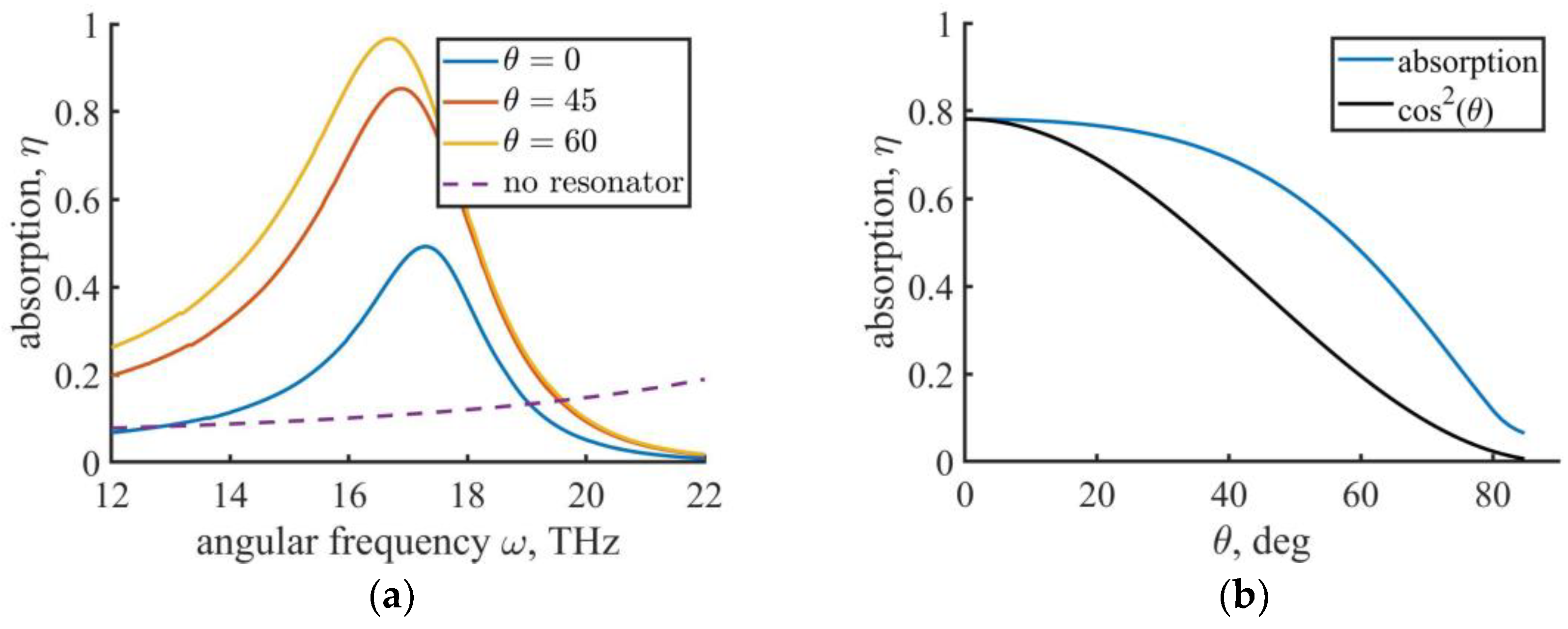
In our study, we propose a method for enhancing the efficiency of uncooled bolometric detectors, whose sensitivity is much smaller than that of cooled ones (where it is possible to detect single photons) and can be different for different types of sensing elements. If we are talking about the normal incidence of radiation (for which TE and TM cases are indistinguishable), the presence of a dielectric layer with specific parameters allows one to detect radiation more efficiently. To prove that statement, we provide the numerical calculation of signal absorption in the structure with a single conducting layer but no dielectric layer (see dashed line in Figure 3a). One can see that in this case, the level of signal absorption is much lower in a given frequency band. Thus, one can conclude that the proposed method can improve detection efficiency by an order of magnitude for resonant frequencies. In other words, minimum detectable energy can be reduced by order.
Further, we have to mention that the discussed problem is multiparametric, so we are starting the discussion with the numerical calculations of the absorption versus frequency of the incident radiation for three different angles of incidence: and for the TE wave (see Figure 3a). In (1), one can consider the quantity where represents a wavelength in the z-direction [25]. So, the increasing incidence angle results in an increase of , and as a consequence, resonant frequencies will be shifted to higher values. Thus, the effect of resonance shifting in the TE wave leads to an inevitable decrease in signal absorption at a given frequency for inclined incidence. Similar results are also shown in [28].
The results obtained in Figure 3a enable us to demonstrate the dependence of the absorbed energy fraction on the angle of incidence of THz radiation. One can see that the absorption is kept at ~80% level for angles of incidence from 0 to 30 degrees (see Figure 3b). Also, the absorption for the angle of 60 degrees turned out to be equal to 50%, which is a more pronounced effect than that of the regular angular dependence.
Now we are focusing on the TM case, where ENZ materials can play a significant role. TM-waves are known to have an effective coupling of the z-component of electric field strength with the plasma wave when and the transport frequency is comparatively low. This is the case when ENZ layers appear. Plasma resonance results in a significant enhancement of the electric field strength within the ENZ region, which in turn leads to efficient absorption of the energy of electromagnetic waves. In our scheme, ENZ areas exist for a wide range of frequencies ( s−1), but for rather low frequencies, the thickness of ENZ areas is too small (since the thickness of ENZ areas is determined by the steepness of the derivative , where , the decrease of leads to increase of the derivative thus narrowing ENZ area) that we are expecting insignificant contribution to the total absorption of TM wave due to the plasma resonance effect. And this is the case for calculations with parameters discussed above (see Figure 4a, in which ENZ areas are marked).
In Figure 4b, you can see the absorption of the x- and z-components of the electric field strength and the total absorption for the TM case depending on the radiation frequency for three different angles of incidence: 0, 30, and 60 deg from top to bottom. field component absorption in the TM wave is similar to the TE-wave, so one can see the same effect of shifting resonances to higher values. The absorption curve of the field component has a relatively complex form, depending on the type of complex permittivity function. The increase in absorption at higher frequencies can be understood from the analysis in (4). Let us fix the doping level at its maximum value (correspondingly, s−1) and analyze the real part of permittivity. Resonance induced by the “dielectric-conductor” resonant structure occurs at s−1. For this frequency, the real part of permittivity and the corresponding ENZ areas (see Figure 4a) are so narrow that they have no influence on the total absorption. If we move to higher frequencies, becomes less negative at first and the corresponding ENZ areas become wider, thus increasing the total absorption. When reaches for the fixed two ENZ areas merge into one wide ENZ area for which plasma resonance is more pronounced. Then, the absorption reaches its peak for frequency, which can be defined as from . This is the case for s−1 for which you can see the maximum absorption for component (see Figure 4b). As was established in Introduction, we define the ENZ region as . Thus, in order to determine the spectral area where maximum of absorption occurs. One has to solve the double inequality: or . The solution is s−1. We mark this spectral region in the Figure 4b. We have to mention that the increase in absorption for component has nothing to do with the resonant frequencies. We can state that for the chosen parameters, the resonance caused by the “dielectric-conductor” resonant structure and the enhancement of absorption due to the presence of ENZ areas turn out to be in different spectral ranges. For the three-periodic structure, we managed to provide the situation when significant enhancement due to the presence of ENZ areas occurs near the resonant frequency, so in Section 3.2, we will discuss this case.
In Figure 4c, we can see the dependence of the fraction of the absorbed power on the angle of incidence for the TM case. As was expected, the role of the component is insignificant in this case.
3.2. Absorption Results for the Case with Three Dielectric Layers
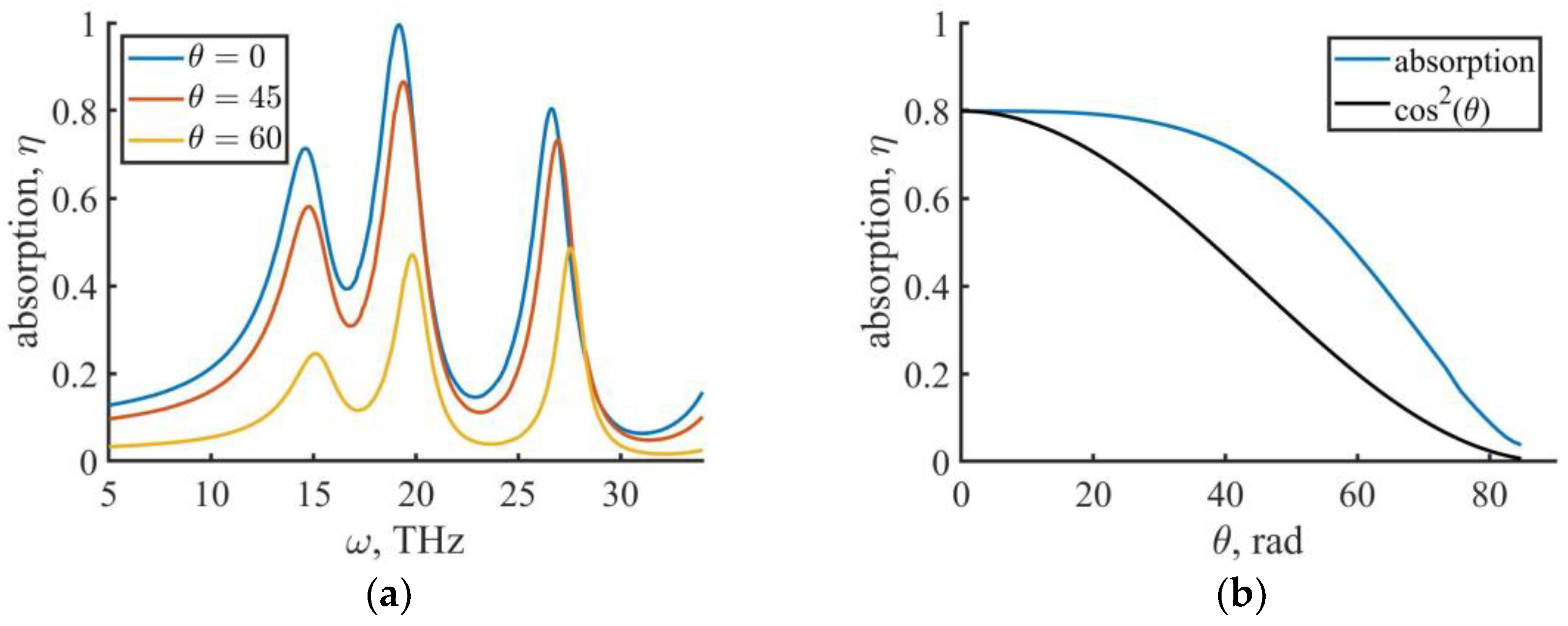
When we consider the structure consisting of three dielectric layers, some kind of spectral zone instead of a single resonant frequency is created. It was discussed in our previous studies [18,19,20]. Shortly, if we have three bonded resonators, three absorption peaks will be formed (see Figure 5a and Figure 6b). Because of the complex type of structure, these peaks have different heights, so let us consider the middle one for the following calculations.
As before, we start the discussion of the calculation results for the structure with three dielectric layers in the TE case. Figure 5a shows the dependence of absorption on the frequency of incident radiation for three different angles: 0, 30, and 60 deg. One can see the shifting of resonances to higher frequencies for larger angles of incidence, as was the case for the single-resonator structure (Figure 3a). Let us fix the frequency s−1 corresponding to the middle absorption peak and plot the dependence of absorption versus the angle of incidence. As you can see in Figure 5b, we managed to fix the absorption at 80% for incident angles from 0 to 40 deg.
Further, we consider the TM case. As it was mentioned above, the z-component of the electric field is known to have an effective coupling with plasma waves in ENZ materials. In the previous section, we stated that for the structure consisting of one dielectric layer under the absorbing layers for chosen parameters, ENZ areas are too narrow to have a visible effect on the total absorption. In the case of three dielectric layers, ENZ areas are narrow as well, but now we have six ENZ areas (see Figure 6a for which ENZ areas are marked) instead of two as in Section 3.1. Considering the component in Figure 6b, one can see the increase in absorption near the resonant frequency. The mechanism of this phenomenon is the same as it was for the case with one resonator. More specifically, as was discussed above, the maximum absorption for the, component occurs when for the maximum value of the doping level (correspondingly, s−1). Similar to that mentioned in Section 3.1, the spectral range for which the ENZ effect is most significant can be defined as s−1. We mark this spectral range in Figure 6b. For the component in Figure 6b, the absorption peaks are also shifted to higher frequencies for larger angles of incidence, like they were for the TE case.
Now we are ready to discuss Figure 6c, which shows the fraction of the absorbed power versus angle of incidence for the TM case. We show that it is possible to fix the absorption at a level as high as 80% of the incident radiation flux for the range of incident angles from 0 to 40 degrees. You can also see that in the case of 3 resonators (or 6 ENZ areas) component makes a more significant contribution to the total absorption as we now have more ENZ areas where radiation can be efficiently absorbed. Also, the effect of the presence of ENZ areas is more pronounced than that in the case of a single dielectric layer since, for the studied configuration, we managed to provide a situation in which the resonance caused by the “dielectric-conductor” resonant structure and the enhancement of absorption due to the presence of ENZ areas turn out to be in the same spectral range. Thus, the results show that effective absorption over a wide range of incidence angles is possible if both resonance effects occur in close frequency regions, thus complementing each other. Since the spectral region of resonance absorption expands as the number of layers in the heterostructure increases, the authors believe that in this case it will be easier to provide a combination of the two effects.
4. Conclusions
To sum up, our study demonstrates the possibility of developing a THz bolometric detection method that ensures high energy absorption for a wide range of angles of incidence. Embedding the dielectric layer (one or a sequence) behind the absorbing layer provides resonant enhancement of wave field amplitude inside the structure if the frequency of incident radiation coincides with one of the resonator’s eigenmodes. Under the inclined wave incidence, this effect takes place for TE waves and, component of the TM wave in our geometry. These waves’ propagation is similar to each other since, in both cases, the electric field strength vector is perpendicular to the plane of incidence (parallel to the structure surface). Specifics of the TM wave are the presence of a, component normal to the surface, which can induce an effective coupling with Langmuir oscillations when . In this case, ENZ regions play a crucial role. For field component, plasma resonance when the dielectric permittivity passes through the point results in a significant enhancement of the electric field strength, which in turn leads to efficient absorption of the, component, thereby increasing the total absorption in the case of the TM wave. For the TE wave, there is no z-component that can interact effectively with the plasma wave.
According to our simulation results, we managed to provide a structure based on a doped and undoped GaAs lattice that ensures stable absorption at the level of 80% of incident radiation flux for the range of incident angles from 0 to 40 degrees for both TE and TM waves. Also, the studied structure allows one to absorb 50% of the signal energy at 60 degrees of incidence for TE and TM waves. For normal incidence, such a structure provides absorption of up to 100% of the energy of the incident radiation.
We should also stress that regular bolometers are broadband detectors with no frequency selectivity. Since the proposed method allows one to increase absorption significantly for the range of resonant frequencies and practically has no impact on non-resonant frequency detection, the bolometer becomes frequency selective, which can be useful for a number of applications.
Author Contributions
Conceptualization, P.N., A.B. and A.P.; data curation, A.B. and A.P.; formal analysis, A.B. and A.P.; investigation, P.N. and A.B.; methodology, A.P.; software, P.N.; supervision, A.B. and A.P.; validation, A.P.; visualization, P.N.; writing—original draft, P.N.; writing—review and editing, A.B. and A.P. All authors have read and agreed to the published version of the manuscript.
Funding
P.N. is grateful for the support of the Foundation for Development of Theoretical Physics and Mathematics, “BAZIS” (project 22-2-10-20-1). A.B. thanks the Foundation for Scholarships of the RF President SP-3120.2022.3.
Institutional Review Board Statement
Not applicable.
Informed Consent Statement
Not applicable.
Data Availability Statement
Data are contained within the article.
Conflicts of Interest
The authors declare no conflicts of interest.
References
- Chen, Z.; Ma, X.; Zhang, B.; Niu, Z.; Kuang, N.; Chen, W.; Li, L.; Li, S. A survey on terahertz communications. China Commun. 2019, 16, 1–35. [Google Scholar] [CrossRef]
- Sarieddeen, H.; Alouini, M.-S.; Al-Naffouri, T.Y. An Overview of Signal Processing Techniques for Terahertz Communications. Proc. IEEE 2021, 109, 1628–1665. [Google Scholar] [CrossRef]
- Tao, Y.H.; Fitzgerald, A.J.; Wallace, V.P. Non-Contact, Non-Destructive Testing in Various Industrial Sectors with Terahertz Technology. Sensors 2020, 20, 712. [Google Scholar] [CrossRef] [PubMed]
- Liebermeister, L.; Nellen, S.; Kohlhaas, R.; Breuer, S.; Schell, M.; Globisch, B. Ultra-fast, High-Bandwidth Coherent cw THz Spectrometer for Non-destructive Testing. J. Infrared Millim. Terahz. Waves 2019, 40, 288–296. [Google Scholar] [CrossRef]
- Zhou, R.; Wang, C.; Xu, W.; Xie, L. Biological applications of terahertz technology based on nanomaterials and nanostructures. Nanoscale 2019, 11, 3445–3457. [Google Scholar] [CrossRef] [PubMed]
- Gong, A.; Qiu, Y.; Chen, X.; Zhao, Z.; Xia, L.; Shao, Y. Biomedical applications of terahertz technology. Appl. Spectrosc. Rev. 2020, 55, 418–438. [Google Scholar] [CrossRef]
- Ren, A.; Zahid, A.; Fan, D.; Yang, X.; Imran, M.A.; Alomainy, A.; Abbasi, Q.H. State-of-the-art in terahertz sensing for food and water security—A comprehensive review. Trends Food Sci. Technol. 2019, 85, 241–251. [Google Scholar] [CrossRef]
- Tzydynzhapov, G.; Gusikhin, P.; Muravev, V.; Dremin, A.; Nefyodov, Y.; Kukushkin, I. New Real-Time Sub-Terahertz Security Body Scanner. J. Infrared Millim. Terahz. Waves 2020, 41, 632–641. [Google Scholar] [CrossRef]
- Stantchev, R.I.; Yu, X.; Blu, T.; Pickwell-MacPherson, E. Real-time terahertz imaging with a single-pixel detector. Nat. Commun. 2020, 11, 2535. [Google Scholar] [CrossRef]
- Valušis, G.; Lisauskas, A.; Yuan, H.; Knap, W.; Roskos, H.G. Roadmap of Terahertz Imaging 2021. Sensors 2021, 21, 4092. [Google Scholar] [CrossRef]
- Zhang, Y.; Hosono, S.; Nagai, N.; Song, S.H.; Hirakawa, K. Fast and sensitive bolometric terahertz detection at room temperature through thermomechanical transduction. J. Appl. Phys. 2019, 125, 151602. [Google Scholar] [CrossRef]
- Liu, Z.; Liang, Z.; Tang, W.; Xu, X. Design and fabrication of low-deformation micro-bolometers for THz detectors. Infrared Phys. Technol. 2020, 105, 103241. [Google Scholar] [CrossRef]
- Kim, Y.; Kim, D.; Lee, S.H.; Seo, M.; Jung, H.-J.; Kang, B.; Lee, S.-M.; Lee, H.-J. Single-layer metamaterial bolometer for sensitive detection of low-power terahertz waves at room temperature. Opt. Express 2020, 28, 17143–17152. [Google Scholar] [CrossRef] [PubMed]
- Ryger, I.; Lobotka, P.; Steiger, A.; Chromik, S.; Lalinsky, T.; Raida, Z.; Pítra, K.; Zehetner, J.; Spankova, M.; Gazi, S.; et al. Uncooled Antenna-Coupled Microbolometer for Detection of Terahertz Radiation. J. Infrared Millim. Terahz. Waves 2021, 42, 462–478. [Google Scholar] [CrossRef]
- Jin, M.; Wang, Y.; Chai, M.; Chen, C.; Zhao, Z.; He, T. Terahertz detectors based on carbon nanomaterials. Adv. Funct. Mater. 2022, 32, 2107499. [Google Scholar] [CrossRef]
- Perenzoni, M.; Paul, D.J. (Eds.) Physics and Applications of Terahertz Radiation; Springer: New York, NY, USA, 2014; Volume 173, p. 36. [Google Scholar] [CrossRef]
- Bogatskaya, A.V.; Klenov, N.V.; Popov, A.M.; Tereshonok, M.V. Resonance Tunneling of Electromagnetic Waves for Enhancing the Efficiency of Bolometric Photodetectors. Tech. Phys. Lett. 2018, 44, 667–670. [Google Scholar] [CrossRef]
- Schegolev, A.E.; Popov, A.M.; Bogatskaya, A.V.; Nikiforova, P.M.; Tereshonok, M.V.; Klenov, N.V. Detection of Terahertz, Mid- and Near Infrared Radiation by a Multilayer Metal—Insulator Heterostructure. JETP Lett. 2020, 111, 371–375. [Google Scholar] [CrossRef]
- Bogatskaya, A.V.; Klenov, N.V.; Nikiforova, P.M.; Popov, A.M.; Schegolev, A.E. Resonant Bolometric Detection of Broadband Terahertz Signals. Tech. Phys. Lett. 2021, 47, 838–842. [Google Scholar] [CrossRef]
- Bogatskaya, A.V.; Klenov, N.V.; Nikiforova, P.M.; Popov, A.M.; Schegolev, A.E. Features of propagation and absorption of electromagnetic signals in periodic structures of conducting and dielectric layers. Opt. Spectrosc. 2022, 130, 385. [Google Scholar] [CrossRef]
- Luk, T.S.; Campione, S.; Kim, I.; Feng, S.; Jun, Y.C.; Liu, S.; Wright, J.B.; Brener, I.; Catrysse, P.B.; Fan, S.; et al. Directional perfect absorption using deep subwavelength low-permittivity films. Phys. Rev. B 2014, 90, 085411. [Google Scholar] [CrossRef]
- Anopchenko, A.; Tao, L.; Arndt, C.; Lee, H.W.H. Field-effect tunable and broadband epsilon-near-zero perfect absorbers with deep subwavelength thickness. ACS Photonics 2018, 5, 2631–2637. [Google Scholar] [CrossRef]
- Wu, J.; Xie, Z.T.; Sha, Y.; Fu, H.Y.; Li, Q. Epsilon-near-zero photonics: Infinite potentials. Photonics Res. 2021, 9, 1616–1644. [Google Scholar] [CrossRef]
- Reshef, O.; De Leon, I.; Alam, M.Z.; Boyd, R.W. Nonlinear optical effects in epsilon-near-zero media. Nat. Rev. Mater. 2019, 4, 535–551. [Google Scholar] [CrossRef]
- Landau, L.D.; Lifshitz, E.M. Electrodynamics of Continuous Media, 2nd ed.; Pergamon Press: Oxford, UK, 1985; pp. 304–305. [Google Scholar]
- GaAs—Gallium Arsenide. Available online: https://www.ioffe.ru/SVA/NSM/Semicond/GaAs/bandstr.html (accessed on 29 September 2023).
- Maremyanin, K.V.; Parshin, V.V.; Serov, E.A.; Rumyantsev, V.V.; Kudryavtsev, K.E.; Dubinov, A.A.; Fokin, A.P.; Morosov, S.S.; Aleshkin, V.Y.; Glyavin, M.Y.; et al. Investigation into Microwave Absorption in Semiconductors for Frequency-Multiplication Devices and Radiation-Output Control of Continuous and Pulsed Gyrotrons. Semiconductors 2020, 54, 1069–1074. [Google Scholar] [CrossRef]
- Bogatskaya, A.V.; Schegolev, A.E.; Klenov, N.V.; Lobov, E.M.; Tereshonok, M.V.; Popov, A.M. Issues with Modeling a Tunnel Communication Channel through a Plasma Sheath. Sensors 2022, 22, 398. [Google Scholar] [CrossRef]
Figure 1.
(a) 3D scheme of the studied structure. (b) The cases of TE and TM waves for inclined radiation incidence.
Figure 1.
(a) 3D scheme of the studied structure. (b) The cases of TE and TM waves for inclined radiation incidence.

Figure 2.
The scheme of the studied resonant structure consists of (a) one dielectric layer and (b) three dielectric layers. The black curve is the real part of dielectric permittivity, . THz radiation is coming from the left. Areas with represent undoped GaAs layers. Areas with represent doped GaAs layers. To be more specific, we consider areas with as dielectric, with as ENZ, and areas with as conductor. Parameters of the structure: thickness of undoped GaAs mkm, thickness of doped GaAs mkm, s−1, varies from 0 (for undoped GaAs) to s−1 (maximum plasma frequency in the doped GaAs).

Figure 3.
TE case. Fraction of the absorbed power versus (a) frequency of the incident radiation for 3 different angles of incidence: 0, , , normal incidence with no resonator; (b) angle of incidence, calculations are made for resonant frequency s−1.
Figure 3.
TE case. Fraction of the absorbed power versus (a) frequency of the incident radiation for 3 different angles of incidence: 0, , , normal incidence with no resonator; (b) angle of incidence, calculations are made for resonant frequency s−1.

Figure 4.
TM case. (a) Spatial distribution of the electric field strength at the resonant frequency; marked areas indicate ENZ areas. This is the case of the normal incidence (). (b) Fraction of the absorbed power versus frequency of the incident radiation for three different angles of incidence: 0, , from top to bottom. (c) Fraction of the absorbed energy versus angle of incidence. Calculations are made for resonant frequency s−1. The regular angular dependence is also shown in the figure. For (b,c), the legend indicates which component of electric field absorption was calculated.

Figure 5.
TE case. Fraction of the absorbed power versus (a) frequency of the incident radiation for three different angles of incidence: 0, , ; (b) angle of incidence, calculations are made for resonant frequency s−1.
Figure 5.
TE case. Fraction of the absorbed power versus (a) frequency of the incident radiation for three different angles of incidence: 0, , ; (b) angle of incidence, calculations are made for resonant frequency s−1.

Figure 6.
TM case. (a) Spatial distribution of the electric field strength at the resonant frequency; purple areas indicate ENZ areas. This is the case of the normal incidence (). (b) Fraction of the absorbed power versus frequency of the incident radiation for 3 different angles of incidence: 0, , from top to bottom. (c) Fraction of the absorbed energy versus angle of incidence. Calculations are made for resonant frequency s−1. The regular angular dependence is also shown in the figures. For (b,c), the legend indicates which component of electric field absorption was calculated.

Disclaimer/Publisher’s Note: The statements, opinions and data contained in all publications are solely those of the individual author(s) and contributor(s) and not of MDPI and/or the editor(s). MDPI and/or the editor(s) disclaim responsibility for any injury to people or property resulting from any ideas, methods, instructions or products referred to in the content. |
© 2023 by the authors. Licensee MDPI, Basel, Switzerland. This article is an open access article distributed under the terms and conditions of the Creative Commons Attribution (CC BY) license (https://creativecommons.org/licenses/by/4.0/).
Share and Cite
MDPI and ACS Style
Nikiforova, P.; Bogatskaya, A.; Popov, A. Enhanced Bolometric Detection of THz Signals by a Resonant Structure for Inclined Radiation Incidence. Photonics 2024, 11, 42. https://0-doi-org.brum.beds.ac.uk/10.3390/photonics11010042
AMA Style
Nikiforova P, Bogatskaya A, Popov A. Enhanced Bolometric Detection of THz Signals by a Resonant Structure for Inclined Radiation Incidence. Photonics. 2024; 11(1):42. https://0-doi-org.brum.beds.ac.uk/10.3390/photonics11010042
Chicago/Turabian StyleNikiforova, Polina, Anna Bogatskaya, and Alexander Popov. 2024. "Enhanced Bolometric Detection of THz Signals by a Resonant Structure for Inclined Radiation Incidence" Photonics 11, no. 1: 42. https://0-doi-org.brum.beds.ac.uk/10.3390/photonics11010042
Note that from the first issue of 2016, this journal uses article numbers instead of page numbers. See further details here.