Direct Writing of Silicon Oxide Nanopatterns Using Photonic Nanojets
by
Hao Luo
1,2,3, 
Haibo Yu
1,2,*,
Yangdong Wen
1,2,
Jianchen Zheng
1,2,3,
Xiaoduo Wang
1,2 and
Lianqing Liu
1,2,* 1
State Key Laboratory of Robotics, Shenyang Institute of Automation, Chinese Academy of Sciences, Shenyang 110016, China
2
Institutes for Robotics and Intelligent Manufacturing, Chinese Academy of Sciences, Shenyang 110016, China
3
University of Chinese Academy of Sciences, Beijing 100049, China
*
Authors to whom correspondence should be addressed.
Photonics 2021, 8(5), 152; https://0-doi-org.brum.beds.ac.uk/10.3390/photonics8050152
Submission received: 29 March 2021
/
Revised: 26 April 2021
/
Accepted: 29 April 2021
/
Published: 3 May 2021
(This article belongs to the Special Issue Photonic Jet: Science and Application)
Abstract
:The ability to create controllable patterns of micro- and nanostructures on the surface of bulk silicon has widespread application potential. In particular, the direct writing of silicon oxide patterns on silicon via femtosecond laser-induced silicon amorphization has attracted considerable attention owing to its simplicity and high efficiency. However, the direct writing of nanoscale resolution is challenging due to the optical diffraction effect. In this study, we propose a highly efficient, one-step method for preparing silicon oxide nanopatterns on silicon. The proposed method combines femtosecond laser-induced silicon amorphization with a subwavelength-scale beam waist of photonic nanojets. We demonstrate the direct writing of arbitrary nanopatterns via contactless scanning, achieving patterns with a minimum feature size of 310 nm and a height of 120 nm. The proposed method shows potential for the fabrication of multifunctional surfaces, silicon-based chips, and silicon photonics.
1. Introduction
Silicon is a popular material for multiple applications involving photonics [1,2], integrated circuits [3,4], and silicon-based chips [5]. In recent decades, femtosecond lasers have proven to be a promising tool for processing silicon [6,7,8,9,10], reducing manufacturing costs, increasing efficiency, and enabling large-area processing. The contemporary femtosecond laser treatment of silicon surfaces is focused primarily on removing material using an energy higher than that required for silicon ablation threshold to ablate the material in the processing area. Ablation technology can be used to alter surface reflectivity [11,12] and wettability [13,14] as well as manufacture micro-lens arrays [15,16]. Moreover, owing to the heat accumulation effect, femtosecond lasers with high repetition rates can directly pattern silicon oxide patterns on a silicon substrate, which has potential applications in maskless lithography [17] and microfluidics [18].
Methods of breaking the optical diffraction limit should be developed to increase the resolution of femtosecond laser processing. It has been reported that irradiating a microsphere with parallel-polarized light generates a photonic nanojet (PNJ) in the backlight of the microsphere, which has a full width at half-maximum (FWHM) beyond the optical diffraction limit [19,20,21,22], thereby providing a new strategy for femtosecond laser super-resolution processing. A recent study showed that PNJs and femtosecond laser ablation can be combined to improve processing resolution [23,24,25]. Most studies have focused on ablation using PNJs [26]. However, no studies have reported the use of a combination of PNJs and thermal oxidation, which can be applied to directly manufacture silicon oxide nanopatterns on silicon substrates.
In this study, we combined PNJs and silicon amorphization induced by the heat accumulation in a high-repetition-rate femtosecond laser to enhance processing resolution. We directly manufactured silicon oxide nanopatterns (nanodots and nanopatterns with an aspect ratio of 1:2.5 and a characteristic size of 310 nm) on a silicon substrate and analyzed the oxidation of the silicon; the amorphization of silicon was observed after ablation. Finite-difference time-domain (FDTD) software was used to compute the light field distribution as the plane wave passed through the microsphere; the results were consistent with experimental measurements. Thus, this study demonstrated significant improvements in the machining applicability of femtosecond lasers.
2. Materials and Methods
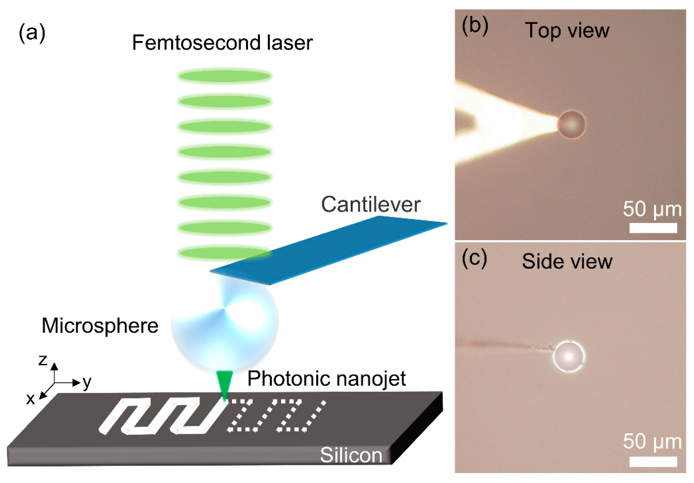
As shown in Figure 1a, the laser incident on the microsphere formed a PNJ upon emerging at the bottom of the microsphere. To avoid microsphere contamination by debris produced during oxidation, we used low-refractive-index (n = 1.47) silica microspheres (diameter = 22 μm, BaseLine, Beijing, China), which ensured that the generated PNJ was focused sufficiently far away from the microspheres. The microspheres were attached to the cantilever of an atomic force microscope (AFM; MLCT, Bruker, Germany) using UV-curable adhesive (NOA63, Edmund Optics) and irradiated for 30 min to fix the attachment (Figure 1b,c) [27]. The low Young’s modulus of the MLCT probe ensured that the microspheres and the cantilever were not damaged when the probe touched the surface of the substrate during processing. The AFM probe and the sample were placed on piezoelectric ceramic transducers to accurately control the distance between the sample and the microsphere to an accuracy of 0.4 nm.
The laser beam was focused through an objective lens (NA = 0.3, MPlanFLN, Olympus) and irradiated onto the microsphere to maximize the laser energy. We used a femtosecond laser (PHAROS-6W, Light Conversion) with a wavelength of 515 nm, pulse duration of 290 fs, and a maximum repetition rate of 200 kHz. The high repetition rate facilitated heat accumulation on the silicon surface, thus accelerating the oxidation. In this experiment, the repetition frequency was fixed at 200 kHz, and the scanning speed was 10 μm/s.
We used Si<100> substrates, which were cleaned with a solution of ammonia, hydrogen peroxide, and ultrapure water at a ratio of 1:1:5. In addition, ultrasonic treatment was performed for 5 min at 50 °C to remove impurities generated during processing. All experimental results were obtained via AFM (Dimension Icon, Bruker) or scanning electron microscopy (SEM; Zeiss EVO MA10). Prior to SEM characterization, the samples were coated with a gold layer (approximate thickness of 30 nm) using a magnetron sputtering instrument.
In addition to the experimental characterization, optical field distribution was simulated using the FDTD computational technique. The simulations were performed for an area of 60 µm × 30 μm, mesh size of λ/100, and the boundary matching layers were set as perfect absorption layers to ensure accuracy. The incident light was a plane wave with a wavelength of 515 nm. The refractive indices of the microsphere (diameter = 22 µm) and the background medium were set as 1.47 and 1, respectively. The simulation conditions were consistent with those of the experiment.
3. Results and Discussion
3.1. Process of Silicon Oxide Microstructure Induced by PNJ
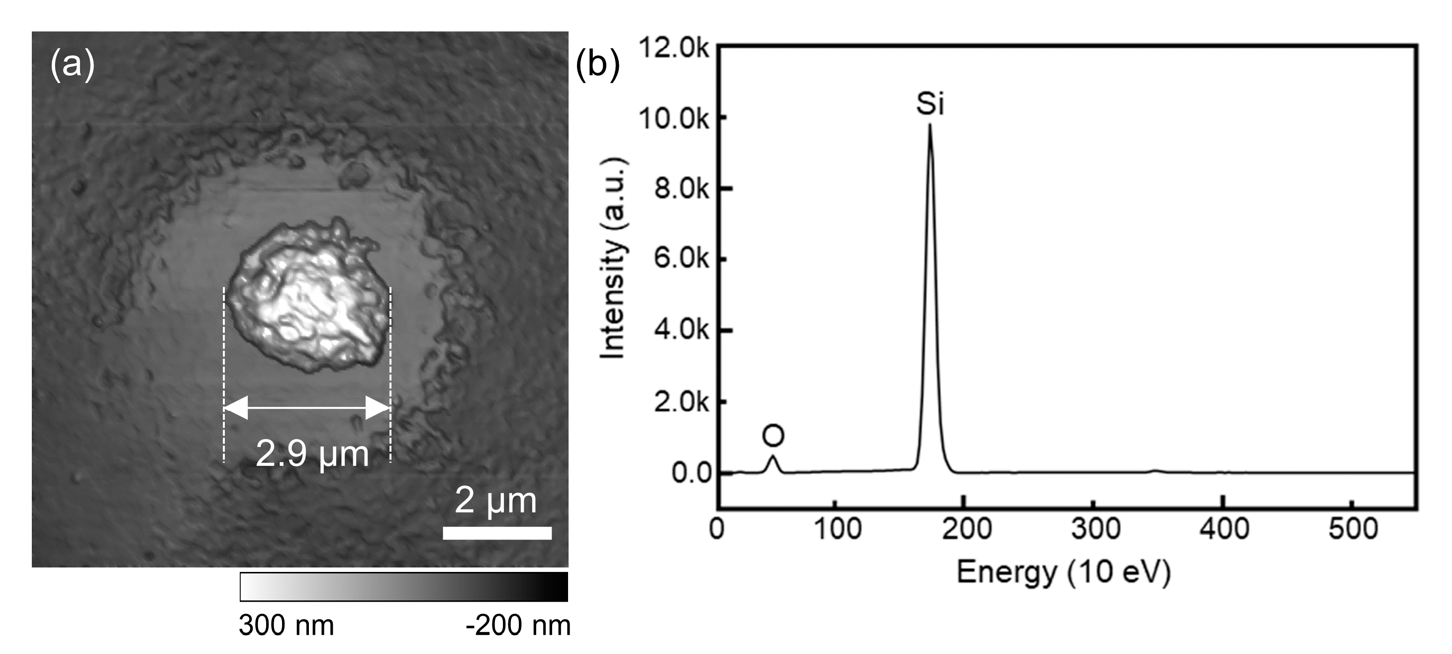
A convex structure, diameter of approximately 2.9 μm was achieved by directly focusing a 200 kHz femtosecond laser (Figure 2a). Energy-dispersive spectroscopy (EDS) was used to analyze the constitution of the convex structure, thus showing that a femtosecond laser with a high repetition rate can oxidize silicon to silicon oxide (Figure 2b) [17,28,29]. In order to improve the manufacturing resolution, microspheres were used to generate PNJ.
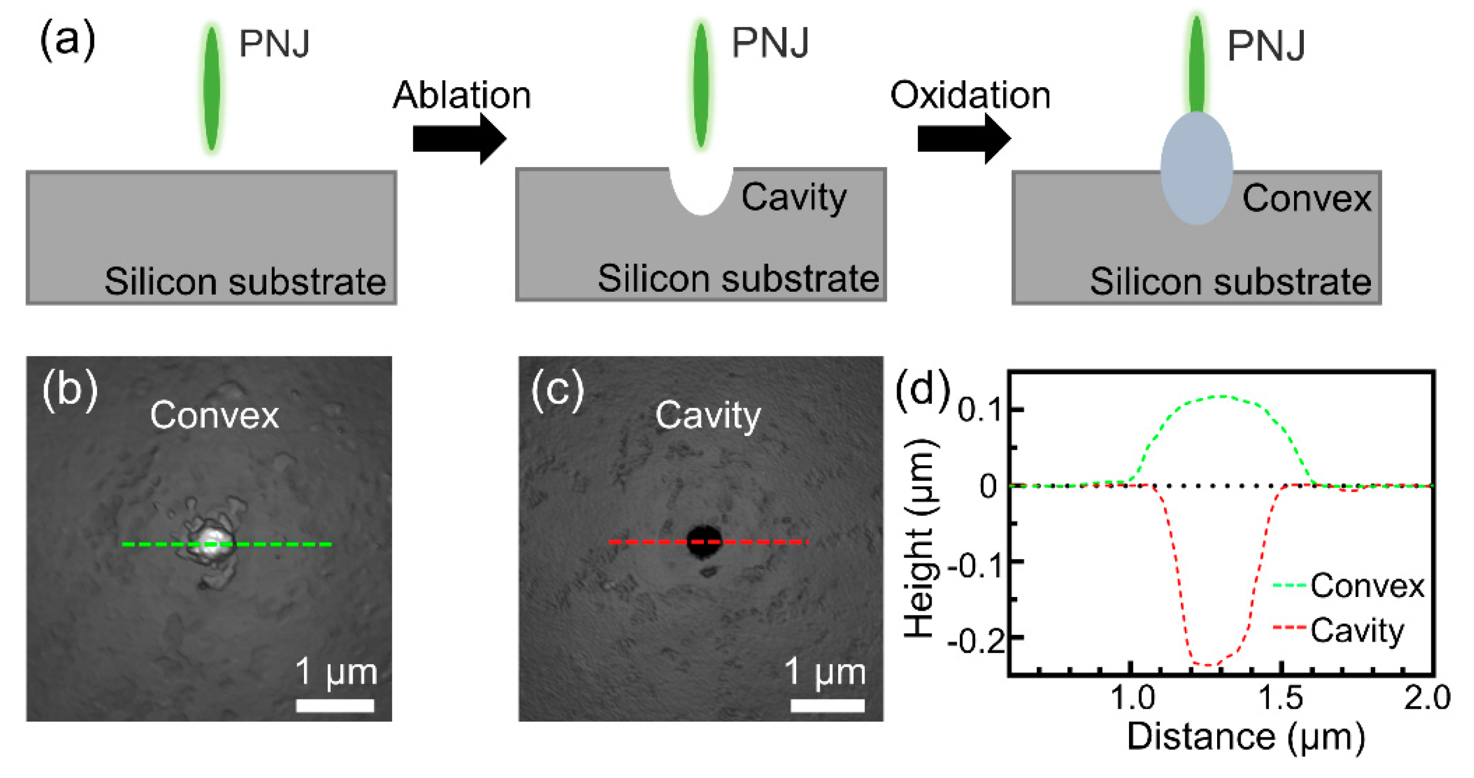
Figure 3a shows a schematic of the oxidation of the silicon substrate by the PNJ. Owing to the extremely high energy density of the PNJ, the silicon substrate was ablated, forming micro/nanocavities [24]. After the formation of the micro-/nanocavities, there was not sufficient space for the heat accumulated to dissipate because of the high-repetition laser pulses, causing the temperature in the pores to be higher than the temperature oxidating the silicon substrate. The resulting oxidation converted the silicon to silica. In addition, because the ablation threshold of silicon is much lower than that of silicon dioxide [30,31], convex silicon oxide formed on the silicon substrate (Figure 3b).
Hydrofluoric acid (HF) is strongly corrosive to silicon oxides; therefore, we used 10% HF to remove the convex oxide. This process created a cavity with an FWHM of 265 nm on the silicon substrate (Figure 3c), confirming that the main component of the convex structure induced by the high-repetition-rate femtosecond laser is silicon oxide.
The morphologies of the convex structure and the cavity were analyzed using AFM, as shown in Figure 3d. The convex structure has an FWHM of 310 nm, and the ratio of height to width is approximately 1:2.5. Note that the convex structure was formed using direct laser irradiation without introducing an etching reagent. Compared without microspheres (Figure 2a), the character size of the manufactured features is greater by an order of magnitude.
3.2. Simulation Analysis of PNJ
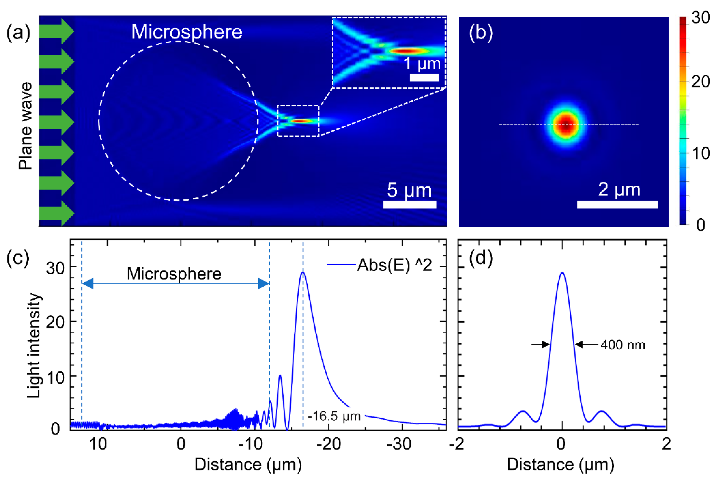
To analyze the PNJ processing mechanism in greater detail, we conducted a simulation using the experimental conditions to calculate the light field distribution generated by the femtosecond laser as it passes through the microsphere (Figure 4). When the PNJ emerges from the microsphere, the local light intensity is significantly enhanced (Figure 4a). The energy distribution of the light field along the z-axis is shown in Figure 4b. Starting from the direction of incidence (indicated by the green arrows in Figure 4a), the energy of the light field oscillates violently because of the interference between the reflected and incident light [32]. Outside the microsphere, the energy of the light field increases rapidly and is the highest at a distance of 4.5 μm from the microsphere, at which point the energy intensity is approximately 30 times greater than that of the incident light energy. However, the energy decreases rapidly as the distance continues to increase. The length of the PNJ is approximately 5 μm, exceeding the focal spot length of the high-NA objective lens, which has a longer working distance. In addition, we analyzed the energy profile in the xy-plane at the maximum light intensity, as shown in Figure 4c,d. A side lobe can be observed near the PNJ, which has an intensity equal to approximately one-third that of the PNJ. The FWHM of the PNJ is approximately 400 nm (Figure 4d), which corresponds to the size of the machined protrusion.
3.3. Effect of Laser Power on the Size of the Oxidized Region
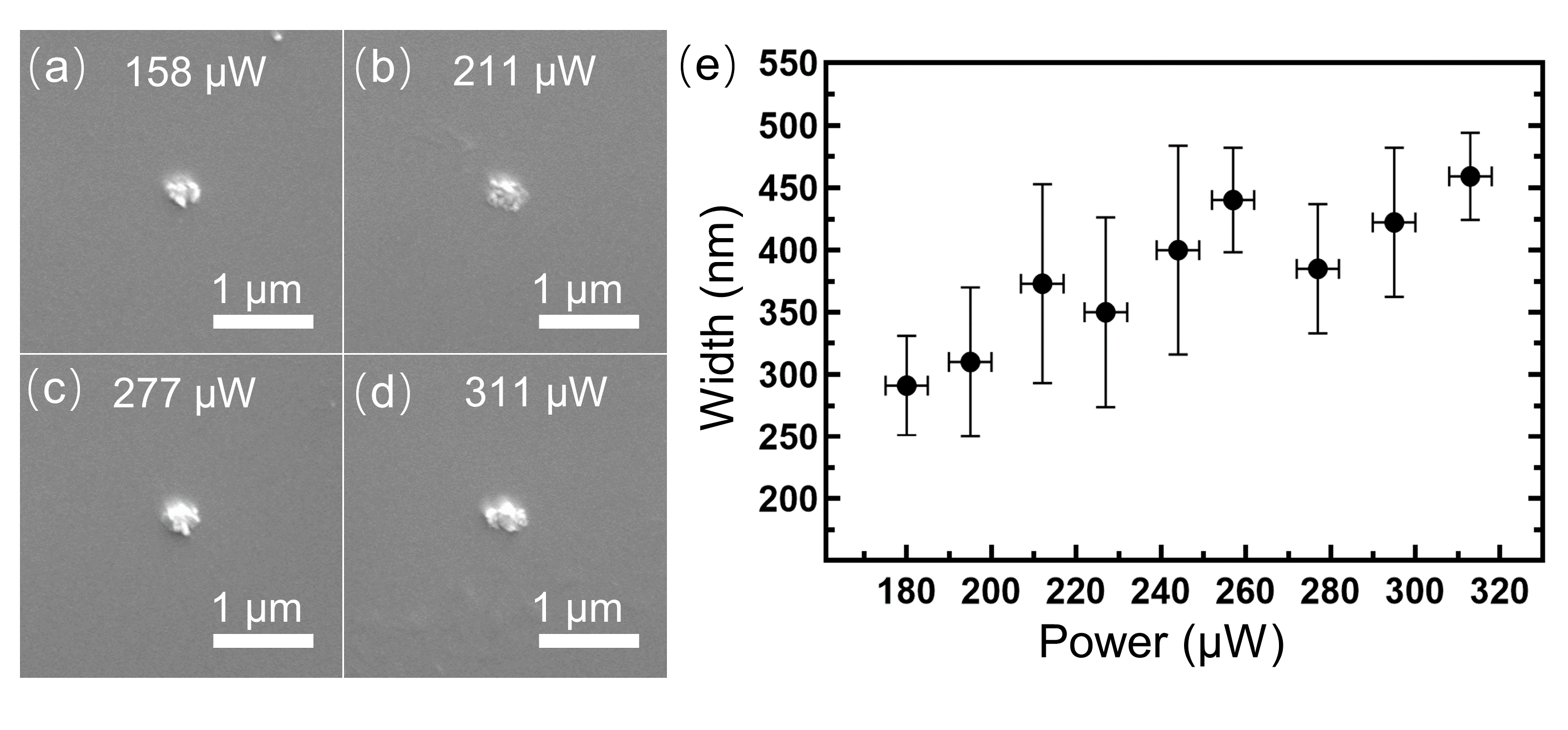
Energy, as an important parameter in laser processing, determines the size of the machined structures. The relationship between the energy density of the PNJ and the size of the oxidation region for femtosecond lasers of different powers is shown in Figure 5. Specifically, Figure 5a–d show SEM images corresponding to laser powers of 158, 211, 277, and 331 μW, respectively. The protruding surface was relatively rough, owing to uneven oxidation. In part, this is due to the accumulation of oxidized debris generated during the ablation. As in ordinary laser processing, a higher energy density results in larger feature sizes (Figure 5e). The minimum feature size obtained during the experiment was 290 nm. Owing to the nonlinear absorption of silicon and ablation fluence threshold [33], the FWHM of the convex structure was smaller than the simulated value, which is consistent with the simulation results. In addition, Figure 4b shows that the energy distribution at the peak PNJ intensity is approximately Gaussian. Therefore, by combining accurate laser energy control with the nonlinear absorption of silicon, high-resolution silica protrusions can be achieved and used to create patterns.
3.4. Directly Writing Arbitrary Silicon Dioxide Pattern
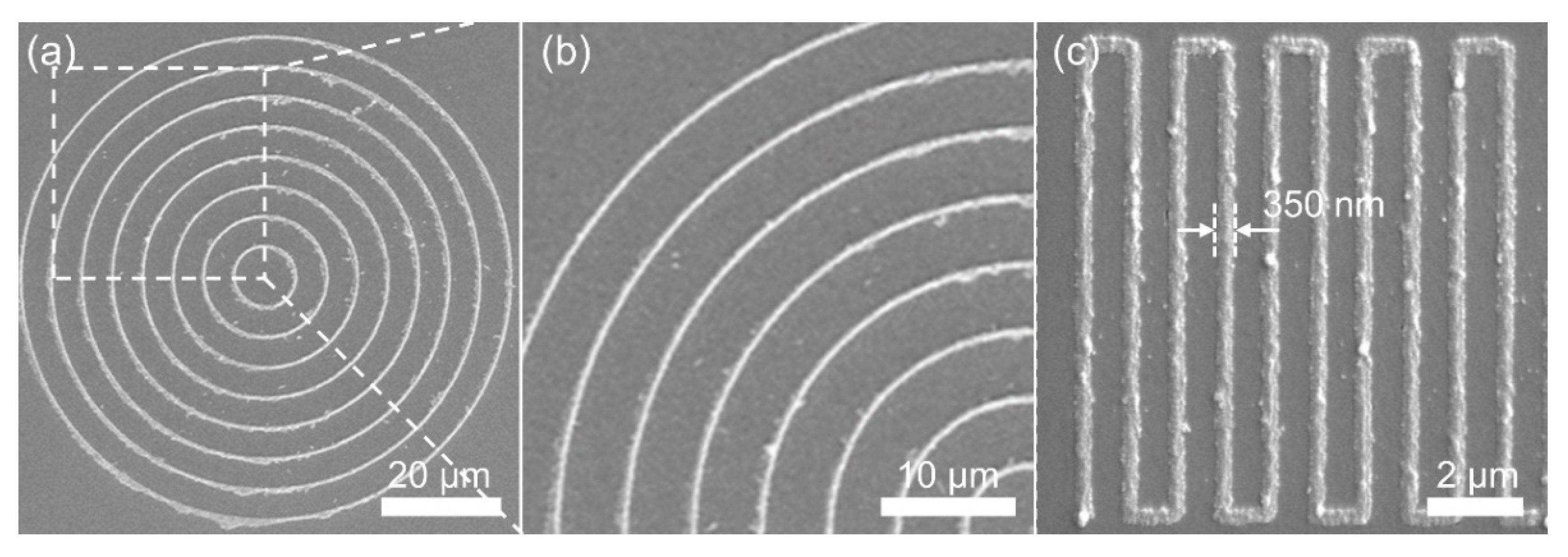
Finally, we applied the one-step process to realize direct silica patterning by scanning. The position of the microsphere was maintained, while the piezoelectric ceramic transducer was programmed to trace an expected path. Note that the substrate was separated from the microspheres by an approximate distance of 4.5 µm, with this noncontact processing method protecting the microspheres from surface splashes. The pattern shown in the SEM image in Figure 6 was produced using a laser power of 158 μW, a scanning speed of 10 µm/s, and a laser repetition frequency of 200 kHz. We achieved a silicon oxide pattern preparation of 100 µm × 100 μm (Figure 6a), and the width of the prepared features was approximately 350 nm (Figure 6c). Owing to the nonuniformity of oxidation, achieving highly uniform patterns via this approach is difficult. Nevertheless, it may be possible to reduce the roughness of silicon dioxide nanowires by using a femtosecond laser with a higher repetition rate.
4. Conclusions
This study demonstrates the direct writing of silicon oxide nanopatterns on a silicon substrate with an FWHM of approximately 350 μm and an aspect ratio of 1:2.5. By using the FWHM of the PNJ to overcome the optical diffraction limit, along with using a high-repetition-rate femtosecond laser, the patterning of silica nanostructures on a silicon substrate was achieved via a one-step process. The minimum size of the prepared nanopattern is approximately 310 nm. With further refinement, we believe that the combination of nonlinear material absorption and the precise laser energy control can be used to fabricate silica patterns with a resolution <300 nm or better. As such, the approach described herein has the potential to be utilized for applications requiring silicon-based chips and optical waveguides.
Author Contributions
L.L., H.L. and H.Y. conceived the basic idea of this study and designed its experiments; H.L. and X.W. designed the optical system and performed the experiments; H.L., H.Y. and L.L. analyzed the data and co-wrote this paper; L.L. and H.Y. supervised the project; J.Z. and Y.W. assisted in the experimental processes. All authors contributed to the general discussion and revision of the manuscript. All authors have read and agreed to the published version of the manuscript.
Funding
This research was funded by National Natural Science Foundation of China (grant numbers 61925307, 61727811, 61973298, 61803366 and 61821005); External Cooperation Program of the Chinese Academy of Sciences (grant number 173321KYSB20170015); CAS Interdisciplinary Innovation Team (JCTD-2019-09); Liaoning Revitalization Talents Program (grant number XLYC1807006); Youth Innovation Promotion Association of the Chinese Academy of Sciences (grant number Y201943).
Data Availability Statement
The data are available from the corresponding author upon reasonable request.
Conflicts of Interest
The authors declare no conflict of interest.
References
- Priolo, F.; Gregorkiewicz, T.; Galli, M.; Krauss, T.F. Silicon nanostructures for photonics and photovoltaics. Nat. Nanotechnol. 2014, 9, 19–32. [Google Scholar] [CrossRef] [PubMed]
- Wu, X.; Pan, X.; Quan, B.; Wang, L. Optical modulation of terahertz behavior in silicon with structured surfaces. Appl. Phys. Lett. 2013, 103, 121112. [Google Scholar] [CrossRef]
- Wang, C.G.; Wu, X.Z.; Di, D.; Dong, P.T.; Xiao, R.; Wang, S.Q. Orientation-dependent nanostructure arrays based on anisotropic silicon wet-etching for repeatable surface-enhanced Raman scattering. Nanoscale 2016, 8, 4672–4680. [Google Scholar] [CrossRef]
- Lin, C.; Huang, N.; Povinelli, M.L. Effect of aperiodicity on the broadband reflection of silicon nanorod structures for photovoltaics. Opt. Express 2012, 20, A125–A132. [Google Scholar] [CrossRef] [PubMed]
- Andersson, H.; Berg, A. Microfabrication and microfluidics for tissue engineering: State of the art and future opportunities. Lab Chip 2004, 4, 98–103. [Google Scholar] [CrossRef]
- Malinauskas, M.; Žukauskas, A.; Hasegawa, S.; Hayasaki, Y.; Mizeikis, V.; Buividas, R.; Juodkazis, S. Ultrafast laser processing of materials: From science to industry. Light Sci. Appl. 2016, 5, e16133. [Google Scholar] [CrossRef] [Green Version]
- Sugioka, K.; Cheng, Y. Ultrafast lasers—Reliable tools for advanced materials processing. Light Sci. Appl. 2014, 3, e149. [Google Scholar] [CrossRef]
- Chen, T.; Wang, W.; Tao, T.; Pan, A.; Mei, X. Multi-scale micro-nano structures prepared by laser cleaning assisted laser ablation for broadband ultralow reflectivity silicon surfaces in ambient air. Appl. Surf. Sci. 2020, 509, 145182. [Google Scholar] [CrossRef]
- Vorobyev, A.Y.; Guo, C. Multifunctional surfaces produced by femtosecond laser pulses. J. Appl. Phys. 2015, 117, 033103. [Google Scholar] [CrossRef] [Green Version]
- Chicbkov, B.N.; Momma, C.; Nolte, S. Femtosecond, picosecond and nanosecond laser ablation of solids. Appl. Phys. A 1996, 63, 109–115. [Google Scholar] [CrossRef]
- Zou, T.; Zhao, B.; Xin, W.; Wang, Y.; Wang, B.; Zheng, X.; Xie, H.; Zhang, Z.; Yang, J.; Guo, C. High-speed femtosecond laser plasmonic lithography and reduction of graphene oxide for anisotropic photoresponse. Light Sci. Appl. 2020, 9, 69. [Google Scholar] [CrossRef] [Green Version]
- Chen, T.; Wang, W.; Tao, T.; Pan, A.; Mei, X. Broad-Band Ultra-Low-Reflectivity Multiscale Micro–Nano Structures by the Combination of Femtosecond Laser Ablation and In Situ Deposition. ACS Appl. Mater. Interfaces 2020, 12, 49265–49274. [Google Scholar] [CrossRef]
- Huo, J.; Yang, Q.; Yong, J.; Fan, P.; Lu, Y.; Hou, X.; Chen, F. Bubble Passage: Underwater Superaerophobicity/Superaerophilicity and Unidirectional Bubble Passage Based on the Femtosecond Laser-Structured Stainless Steel Mesh. Adv. Mater. Interfaces 2020, 7, 2070077. [Google Scholar] [CrossRef]
- Zhan, Z.; ElKabbash, M.; Cheng, J.; Zhang, J.; Singh, S.; Guo, C. Highly Floatable Superhydrophobic Metallic Assembly for Aquatic Applications. ACS Appl. Mater. Interfaces 2019, 11, 48512–48517. [Google Scholar] [CrossRef] [PubMed] [Green Version]
- Bian, H.; Wei, Y.; Yang, Q.; Chen, F.; Zhang, F.; Du, G.; Yong, J.; Hou, X. Direct fabrication of compound-eye microlens array on curved surfaces by a facile femtosecond laser enhanced wet etching process. Appl. Phys. Lett. 2016, 109, 221109. [Google Scholar] [CrossRef] [Green Version]
- Cao, J.J.; Hou, Z.S.; Tian, Z.N.; Hua, J.G.; Zhang, Y.L.; Chen, Q.D. Bioinspired Zoom Compound Eyes Enable Variable-Focus Imaging. ACS Appl. Mater. Interfaces 2020, 12, 10107–10117. [Google Scholar] [CrossRef] [PubMed]
- Liu, X.Q.; Yu, L.; Ma, Z.C.; Chen, Q.D. Silicon three-dimensional structures fabricated by femtosecond laser modification with dry etching. Appl. Opt. 2017, 56, 2157–2161. [Google Scholar] [CrossRef]
- Kumar, K.; Lee, K.K.C.; Herman, P.R.; Nogami, J.; Kherani, N.P. Femtosecond laser direct hard mask writing for selective facile micron-scale inverted-pyramid patterning of silicon. Appl. Phys. Lett. 2012, 101, 222106. [Google Scholar] [CrossRef]
- Ferrand, P.; Wenger, J.; Devilez, A.; Pianta, M.; Stout, B.; Bonod, N.; Popov, E.; Rigneault, H. Direct imaging of photonic nanojets. Opt. Express 2008, 16, 6930–6940. [Google Scholar] [CrossRef] [PubMed]
- Zhu, J.; Goddard, L.L. Spatial control of photonic nanojets. Opt. Express 2016, 24, 30444–30464. [Google Scholar] [CrossRef]
- Kim, M.S.; Lahijani, B.V.; Descharmes, N.; Straubel, J.; Negredo, F.; Rockstuhl, C.; Hayrinen, M.; Kuittinen, M.; Roussey, M.; Herzig, H.P. Subwavelength Focusing of Bloch Surface Waves. ACS Photonics 2017, 4, 1477–1483. [Google Scholar] [CrossRef] [Green Version]
- Wang, Z.; Guo, W.; Li, L.; Luk, B.; Khan, A.; Liu, Z.; Chen, Z.; Hong, M. Optical virtual imaging at 50 nm lateral resolution with a white-light nanoscope. Nat. Commun. 2011, 2, 218. [Google Scholar] [CrossRef] [PubMed] [Green Version]
- Wen, Y.; Wang, F.; Yu, H.; Li, P.; Liu, L.; Li, W.J. Laser-nanomachining by microsphere induced photonic nanojet. Sens. Actuators A Phys. 2017, 258, 115–122. [Google Scholar] [CrossRef]
- Yan, B.; Yue, L.; Monks, J.N.; Yang, X.; Xiong, D.; Jiang, C.; Wang, Z. Superlensing plano-convex-microsphere (PCM) lens for direct laser nano-marking and beyond. Opt. Lett. 2020, 45, 1168–1171. [Google Scholar] [CrossRef] [PubMed]
- Jacassi, A.; Tantussi, F.; Dipalo, M.; Biagini, C.; Maccaferri, N.; Bozzola, A.; Angelis, F.D. Scanning Probe Photonic Nanojet Lithography. ACS Appl. Mater. Interfaces 2017, 9, 32386–32393. [Google Scholar] [CrossRef] [PubMed] [Green Version]
- Darafsheh, A. Photonic nanojets and their applications. J. Phys. Photonics 2021, 3, 022001. [Google Scholar] [CrossRef]
- Wang, F.; Liu, L.; Yu, H.; Wen, Y.; Yu, P.; Liu, Z.; Wang, Y.; Li, W.J. Scanning superlens microscopy for non-invasive large field-of-view visible light nanoscale imaging. Nat. Commun. 2016, 7, 13748. [Google Scholar] [CrossRef]
- Kiani, A.; Venkatakrishnan, K.; Tan, B. Direct laser writing of amorphous silicon on Si-substrate induced by high repetition femtosecond pulses. J. Appl. Phys. 2010, 108, 074907. [Google Scholar] [CrossRef]
- Kiani, A.; Venkatakrishnan, K.; Tan, B. Direct patterning of silicon oxide on Si-substrate induced by femtosecond laser. Opt. Express 2010, 18, 1872–1878. [Google Scholar] [CrossRef]
- Bloembergen, N. Laser-induced electric breakdown in solids. IEEE J. Quantum Electron. 1974, 10, 375. [Google Scholar] [CrossRef]
- Bonse, J.; Baudach, S.; Krüger, J.; Kautek, W.; Lenzner, M. Femtosecond laser ablation of silicon–modification thresholds and morphology. Appl. Phys. A 2002, 74, 19–25. [Google Scholar] [CrossRef]
- Wen, Y.; Yu, H.; Zhao, W.; Wang, F.; Wang, X.; Liu, L.; Li, W.J. Photonic Nanojet Sub-Diffraction Nano-Fabrication With in situ Super-Resolution Imaging. IEEE Trans. Nanotechnol. 2019, 18, 226–233. [Google Scholar] [CrossRef]
- Garcia-Lechuga, M.; Utéza, O.; Sanner, N.; Grojo, D. Evidencing the nonlinearity independence of resolution in femtosecond laser ablation. Opt. Lett. 2020, 45, 952–955. [Google Scholar] [CrossRef] [PubMed]
Figure 1.
(a) Schematic showing the direct writing of silicon oxide patterns on a silicon substrate via a PNJ. (b) Top and (c) side views of a microsphere attached to the cantilever of an AFM. The diameter of the fused silica microspheres (n = 1.47) is approximately 22 μm.
Figure 1.
(a) Schematic showing the direct writing of silicon oxide patterns on a silicon substrate via a PNJ. (b) Top and (c) side views of a microsphere attached to the cantilever of an AFM. The diameter of the fused silica microspheres (n = 1.47) is approximately 22 μm.

Figure 2.
(a) High-repetition-rate femtosecond laser-induced convex structures, directly focused by an object lens (NA = 0.3, MPlanFLN, Olympus). (b) EDS of convex structures showing silicon was oxidized by a femtosecond laser.
Figure 2.
(a) High-repetition-rate femtosecond laser-induced convex structures, directly focused by an object lens (NA = 0.3, MPlanFLN, Olympus). (b) EDS of convex structures showing silicon was oxidized by a femtosecond laser.

Figure 3.
(a) Oxidation of the silicon substrate by the PNJ. (b) AFM image of convex silicon oxide induced by the PNJ. (c) AFM image showing the cavity etched from silicon oxide on silicon with 10% HF. (d) Cross-sectional views of the dotted lines in (b,c).
Figure 3.
(a) Oxidation of the silicon substrate by the PNJ. (b) AFM image of convex silicon oxide induced by the PNJ. (c) AFM image showing the cavity etched from silicon oxide on silicon with 10% HF. (d) Cross-sectional views of the dotted lines in (b,c).

Figure 4.
FDTD simulation of the light field distribution of the PNJ. (a) Setup of the PNJ simulation. The incident light intensity was normalized, with the color bar representing the scaled light intensity. The inset shows the magnified PNJ. (b) The light field distribution in the xy-plane of the PNJ. (c) The light field distribution along the z-axis of the PNJ. The horizontal axis represents distance, and the vertical axis represents the energy intensity of the light field. The center of the microsphere coincides with the zero point of the horizontal axis. (d) Prolife centered about the dotted line in (b).

Figure 5.
Influence of energy density on the machined feature size with microspheres. (a–d) SEM images of silicon substrates irradiated with lasers with powers of 158, 211, 277, and 331 μW, respectively. (e) Width of the oxidation-induced convex silicon oxide structures as a function of laser power.

Figure 6.
SEM image of silicon oxide nanopatterns, (a,b) concentric circles and (c) grid.

Publisher’s Note: MDPI stays neutral with regard to jurisdictional claims in published maps and institutional affiliations. |
© 2021 by the authors. Licensee MDPI, Basel, Switzerland. This article is an open access article distributed under the terms and conditions of the Creative Commons Attribution (CC BY) license (https://creativecommons.org/licenses/by/4.0/).
Share and Cite
MDPI and ACS Style
Luo, H.; Yu, H.; Wen, Y.; Zheng, J.; Wang, X.; Liu, L. Direct Writing of Silicon Oxide Nanopatterns Using Photonic Nanojets. Photonics 2021, 8, 152. https://0-doi-org.brum.beds.ac.uk/10.3390/photonics8050152
AMA Style
Luo H, Yu H, Wen Y, Zheng J, Wang X, Liu L. Direct Writing of Silicon Oxide Nanopatterns Using Photonic Nanojets. Photonics. 2021; 8(5):152. https://0-doi-org.brum.beds.ac.uk/10.3390/photonics8050152
Chicago/Turabian StyleLuo, Hao, Haibo Yu, Yangdong Wen, Jianchen Zheng, Xiaoduo Wang, and Lianqing Liu. 2021. "Direct Writing of Silicon Oxide Nanopatterns Using Photonic Nanojets" Photonics 8, no. 5: 152. https://0-doi-org.brum.beds.ac.uk/10.3390/photonics8050152
Note that from the first issue of 2016, this journal uses article numbers instead of page numbers. See further details here.