
Heat-Induced Fragmentation and Adhesive Behaviour of Gold Nanowires for Surface-Enhanced Raman Scattering Substrates
 , , , , and
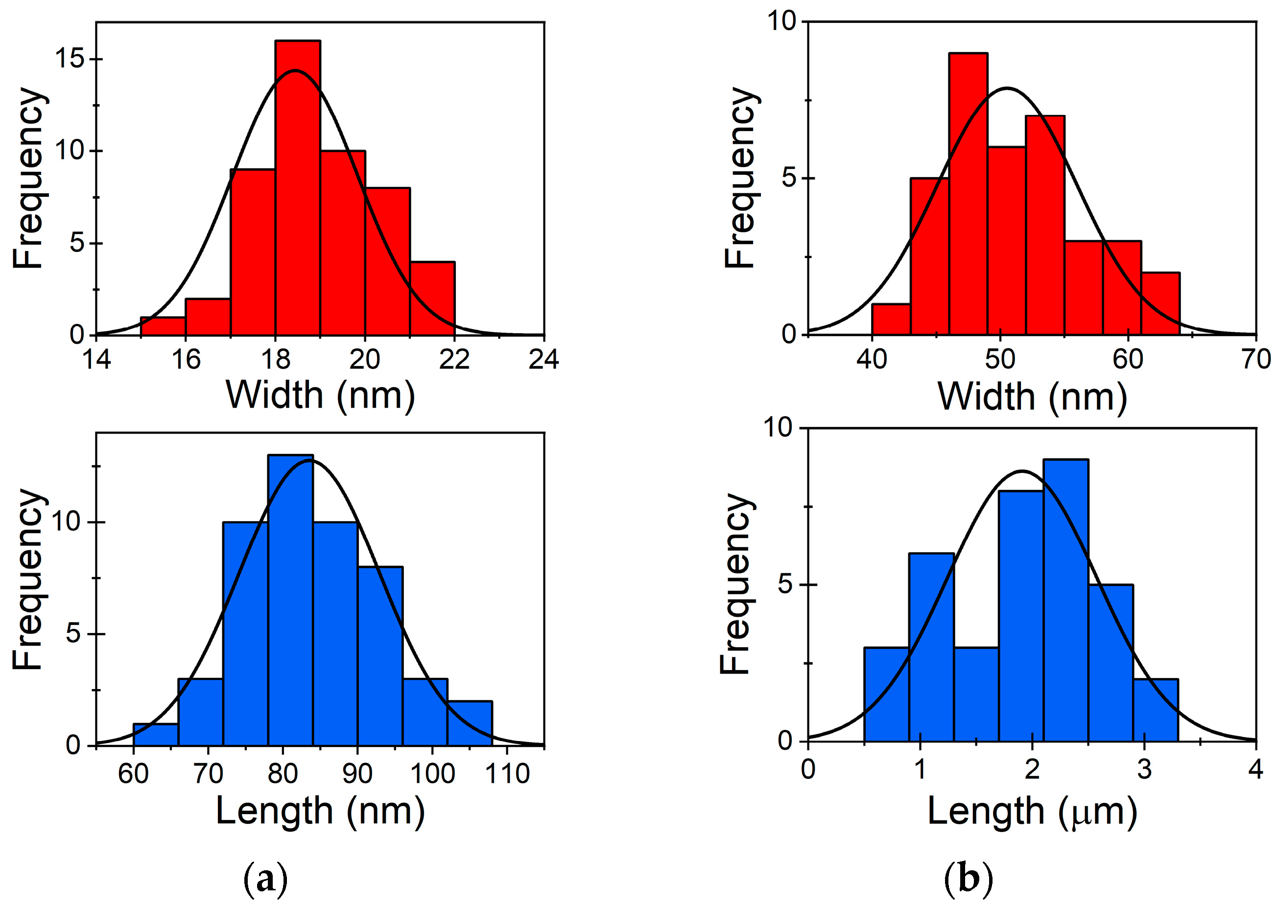
Abstract
:1. Introduction
2. Materials and Methods
2.1. Materials
2.2. Sample Preparation
2.3. Annealing
2.4. Characterisation
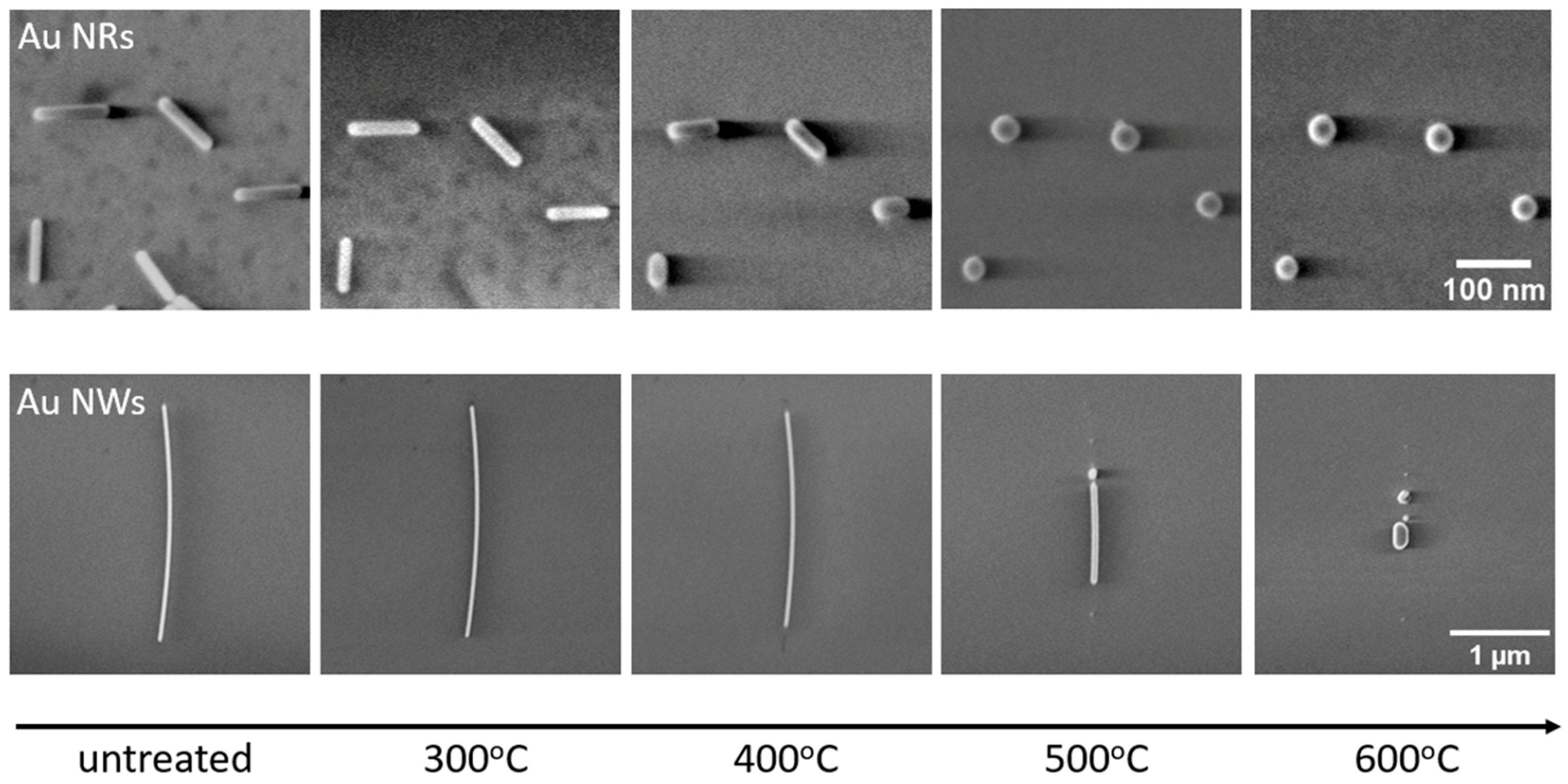
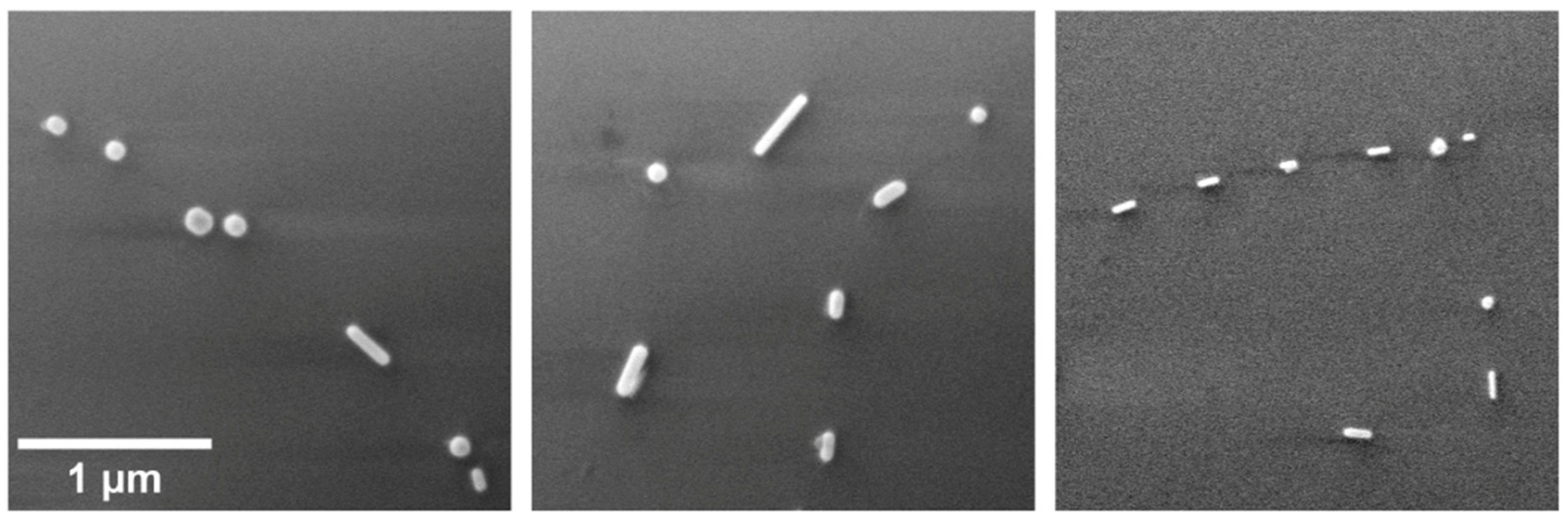
3. Results
3.1. Au NP Characterisation
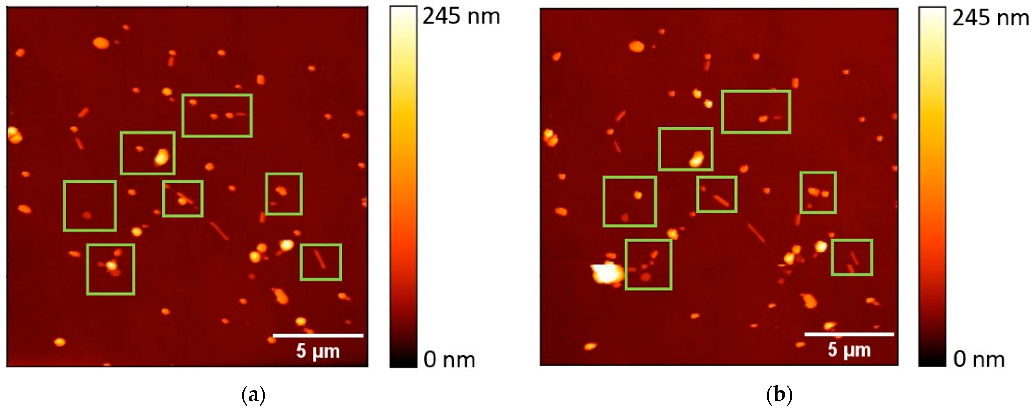
3.2. AFM Measurements
3.3. Raman Measurements
4. Conclusions
Supplementary Materials
Author Contributions
Funding
Data Availability Statement
Conflicts of Interest
References
- Hu, Q.; Zhao, G.; Guo, H.; He, J.; Liu, H.; Wu, R.; Zhang, C. Preparation and SERS Performance of Gold Nanoparticles-Decorated Patterned Silicon Substrate. Appl. Surf. Sci. 2023, 638, 157966. [Google Scholar] [CrossRef]
- Augustine, S.; Saini, M.; Sooraj, K.P.; Parida, B.K.; Hans, S.; Pachchigar, V.; Satpati, B.; Ranjan, M. Au/Ag SERS Active Substrate for Broader Wavelength Excitation. Opt. Mater. 2023, 135, 113319. [Google Scholar] [CrossRef]
- Halas, N.J.; Lal, S.; Chang, W.-S.; Link, S.; Nordlander, P. Plasmons in Strongly Coupled Metallic Nanostructures. Chem. Rev. 2011, 111, 3913–3961. [Google Scholar] [CrossRef] [PubMed]
- Pedano, M.L.; Li, S.; Schatz, G.C.; Mirkin, C.A. Periodic Electric Field Enhancement Along Gold Rods with Nanogaps. Angew. Chem. Int. Ed. 2009, 49, 78–82. [Google Scholar] [CrossRef] [PubMed]
- Shegai, T.; Brian, B.; Miljković, V.D.; Käll, M. Angular Distribution of Surface-Enhanced Raman Scattering from Individual Au Nanoparticle Aggregates. ACS Nano 2011, 5, 2036–2041. [Google Scholar] [CrossRef] [PubMed]
- Andreiuk, B.; Nicolson, F.; Clark, L.M.; Panikkanvalappil, S.R.; Kenry; Rashidian, M.; Harmsen, S.; Kircher, M.F. Design and Synthesis of Gold Nanostars-Based SERS Nanotags for Bioimaging Applications. Nanotheranostics 2022, 6, 10–30. [Google Scholar] [CrossRef] [PubMed]
- Marques, A.C.; Pinheiro, T.; Morais, M.; Martins, C.; Andrade, A.F.; Martins, R.; Sales, M.G.F.; Fortunato, E. Bottom-up Microwave-Assisted Seed-Mediated Synthesis of Gold Nanoparticles onto Nanocellulose to Boost Stability and High Performance for SERS Applications. Appl. Surf. Sci. 2021, 561, 150060. [Google Scholar] [CrossRef]
- Kapara, A.; Brunton, V.; Graham, D.; Faulds, K. Investigation of Cellular Uptake Mechanism of Functionalised Gold Nanoparticles into Breast Cancer Using SERS. Chem. Sci. 2020, 11, 5819–5829. [Google Scholar] [CrossRef]
- Wu, R.; Jin, Q.; Storey, C.; Collins, J.; Gomard, G.; Lemmer, U.; Canham, L.; Kling, R.; Kaplan, A. Gold Nanoplasmonic Particles in Tunable Porous Silicon 3D Scaffolds for Ultra-Low Concentration Detection by SERS. Nanoscale Horiz. 2021, 6, 781–790. [Google Scholar] [CrossRef] [PubMed]
- Pathak, A.K.; Rahman, B.M.A.; Singh, V.K.; Kumari, S. Sensitivity Enhancement of a Concave Shaped Optical Fiber Refractive Index Sensor Covered with Multiple Au Nanowires. Sensors 2019, 19, 4210. [Google Scholar] [CrossRef]
- Inal, O.; Badilli, U.; Ozkan, A.S.; Mollarasouli, F. Bioactive Hybrid Nanowires for Drug Delivery. Hybrid Nanomater. Drug Deliv. 2022, 269–301. [Google Scholar] [CrossRef]
- Jakhmola, A.; Krishnan, S.; Onesto, V.; Gentile, F.; Profeta, M.; Manikas, A.; Battista, E.; Vecchione, R.; Netti, P.A. Sustainable Synthesis and Theoretical Studies of Polyhedral Gold Nanoparticles Displaying High SERS Activity, NIR Absorption, and Cellular Uptake. Mater. Today Chem. 2022, 26, 101016. [Google Scholar] [CrossRef]
- Fan, J.; Cheng, Y.; Sun, M. Functionalized Gold Nanoparticles: Synthesis, Properties and Biomedical Applications. Chem. Rec. 2020, 20, 1474–1504. [Google Scholar] [CrossRef]
- Li, Z.; Huang, X.; Lu, G. Recent Developments of Flexible and Transparent SERS Substrates. J. Mater. Chem. C 2020, 8, 3956–3969. [Google Scholar] [CrossRef]
- Le Ru, E.C.; Grand, J.; Félidj, N.; Aubard, J.; Lévi, G.; Hohenau, A.; Krenn, J.R.; Blackie, E.; Etchegoin, P.G. Experimental Verification of the SERS Electromagnetic Model beyond the |E|4 Approximation: Polarization Effects. J. Phys. Chem. C 2008, 112, 8117–8121. [Google Scholar] [CrossRef]
- Pal, P.; Bonyár, A.; Veres, M.; Himics, L.; Balázs, L.; Juhász, L.; Csarnovics, I. A Generalized Exponential Relationship between the Surface-Enhanced Raman Scattering (SERS) Efficiency of Gold/Silver Nanoisland Arrangements and Their Non-Dimensional Interparticle Distance/Particle Diameter Ratio. Sens. Actuators A Phys. 2020, 314, 112225. [Google Scholar] [CrossRef]
- Fan, M.; Andrade, G.F.S.; Brolo, A.G. A Review on the Fabrication of Substrates for Surface Enhanced Raman Spectroscopy and Their Applications in Analytical Chemistry. Anal. Chim. Acta 2011, 693, 7–25. [Google Scholar] [CrossRef]
- Bonyár, A.; Csarnovics, I.; Veres, M.; Himics, L.; Csik, A.; Kámán, J.; Balázs, L.; Kökényesi, S. Investigation of the Performance of Thermally Generated Gold Nanoislands for LSPR and SERS Applications. Sens. Actuators B Chem. 2018, 255, 433–439. [Google Scholar] [CrossRef]
- Xu, D.; Wang, Z.; Zhang, S.; Yang, W.; Chen, J. High Performance SERS Substrates Using High Surface Roughness Gold Nanosheets Assembled by Nanowires. Vib. Spectrosc. 2020, 107, 103041. [Google Scholar] [CrossRef]
- Pazos-Pérez, N.; Ni, W.; Schweikart, A.; Alvarez-Puebla, R.A.; Fery, A.; Liz-Marzán, L.M. Highly Uniform SERS Substrates Formed by Wrinkle-Confined Drying of Gold Colloids. Chem. Sci. 2010, 1, 174. [Google Scholar] [CrossRef]
- Hong, S.; Li, X. Optimal Size of Gold Nanoparticles for Surface-Enhanced Raman Spectroscopy under Different Conditions. J. Nanomater. 2013, 2013, 790323. [Google Scholar] [CrossRef]
- Stamplecoskie, K.G.; Scaiano, J.C.; Tiwari, V.S.; Anis, H. Optimal Size of Silver Nanoparticles for Surface-Enhanced Raman Spectroscopy. J. Phys. Chem. C 2011, 115, 1403–1409. [Google Scholar] [CrossRef]
- Njoki, P.N.; Lim, I.-I.S.; Mott, D.; Park, H.-Y.; Khan, B.; Mishra, S.; Sujakumar, R.; Luo, J.; Zhong, C.-J. Size Correlation of Optical and Spectroscopic Properties for Gold Nanoparticles. J. Phys. Chem. C 2007, 111, 14664–14669. [Google Scholar] [CrossRef]
- Moskovits, M. Surface-enhanced Raman Spectroscopy: A Brief Retrospective. J. Raman Spectrosc. 2005, 36, 485–496. [Google Scholar] [CrossRef]
- Bell, S.E.J.; Charron, G.; Cortés, E.; Kneipp, J.; de la Chapelle, M.L.; Langer, J.; Procházka, M.; Tran, V.; Schlücker, S. Towards Reliable and Quantitative Surface-Enhanced Raman Scattering (SERS): From Key Parameters to Good Analytical Practice. Angew. Chem. Int. Ed. 2020, 59, 5454–5462. [Google Scholar] [CrossRef] [PubMed]
- Panariello, L.; Chuen To, K.; Khan, Z.; Wu, G.; Gkogkos, G.; Damilos, S.; Parkin, I.P.; Gavriilidis, A. Kinetics-Based Design of a Flow Platform for Highly Reproducible on Demand Synthesis of Gold Nanoparticles with Controlled Size between 50 and 150 Nm and Their Application in SERS and PIERS Sensing. Chem. Eng. J. 2021, 423, 129069. [Google Scholar] [CrossRef]
- Polyakov, B.; Vlassov, S.; Dorogin, L.M.; Butikova, J.; Antsov, M.; Oras, S.; Lõhmus, R.; Kink, I. Manipulation of Nanoparticles of Different Shapes inside a Scanning Electron Microscope. Beilstein J. Nanotechnol. 2014, 5, 133–140. [Google Scholar] [CrossRef] [PubMed]
- Oras, S.; Vlassov, S.; Vigonski, S.; Polyakov, B.; Antsov, M.; Zadin, V.; Lõhmus, R.; Mougin, K. The Effect of Heat Treatment on the Morphology and Mobility of Au Nanoparticles. Beilstein J. Nanotechnol. 2020, 11, 61–67. [Google Scholar] [CrossRef]
- Granberg, F.; Parviainen, S.; Djurabekova, F.; Nordlund, K. Investigation of the Thermal Stability of Cu Nanowires Using Atomistic Simulations. J. Appl. Phys. 2014, 115, 213518. [Google Scholar] [CrossRef]
- Vigonski, S.; Jansson, V.; Vlassov, S.; Polyakov, B.; Baibuz, E.; Oras, S.; Aabloo, A.; Djurabekova, F.; Zadin, V. Au Nanowire Junction Breakup through Surface Atom Diffusion. Nanotechnology 2017, 29, 015704. [Google Scholar] [CrossRef]
- Kim, F.; Sohn, K.; Wu, J.; Huang, J. Chemical Synthesis of Gold Nanowires in Acidic Solutions. J. Am. Chem. Soc. 2008, 130, 14442–14443. [Google Scholar] [CrossRef]
- Schindelin, J.; Arganda-Carreras, I.; Frise, E.; Kaynig, V.; Longair, M.; Pietzsch, T.; Preibisch, S.; Rueden, C.; Saalfeld, S.; Schmid, B.; et al. Fiji: An Open-Source Platform for Biological-Image Analysis. Nat. Methods 2012, 9, 676–682. [Google Scholar] [CrossRef] [PubMed]
- Anczykowski, B.; Gotsmann, B.; Fuchs, H.; Cleveland, J.P.; Elings, V.B. How to Measure Energy Dissipation in Dynamic Mode Atomic Force Microscopy. Appl. Surf. Sci. 1999, 140, 376–382. [Google Scholar] [CrossRef]
- He, S.; Wu, D.; Chen, S.; Liu, K.; Yang, E.-H.; Tian, F.; Du, H. Au-on-Ag Nanostructure for in-Situ SERS Monitoring of Catalytic Reactions. Nanotechnology 2022, 33, 155701. [Google Scholar] [CrossRef]
- Zhang, Y.; Wen, Y.-H.; Zheng, J.-C.; Zhu, Z.-Z. Energetic and Structural Evolution of Gold Nanowire under Heating Process: A Molecular Dynamics Study. Phys. Lett. A 2009, 373, 3454–3458. [Google Scholar] [CrossRef]
- Sun, Y.; Li, W.; Zhao, L.; Li, F.; Xie, Y.; Yao, W.; Liu, W.; Lin, Z. Simultaneous SERS Detection of Illegal Food Additives Rhodamine B and Basic Orange II Based on Au Nanorod-Incorporated Melamine Foam. Food Chem. 2021, 357, 129741. [Google Scholar] [CrossRef]
- Benz, F.; Chikkaraddy, R.; Salmon, A.; Ohadi, H.; de Nijs, B.; Mertens, J.; Carnegie, C.; Bowman, R.W.; Baumberg, J.J. SERS of Individual Nanoparticles on a Mirror: Size Does Matter, but so Does Shape. J. Phys. Chem. Lett. 2016, 7, 2264–2269. [Google Scholar] [CrossRef]
- Han, X.X.; Rodriguez, R.S.; Haynes, C.L.; Ozaki, Y.; Zhao, B. Surface-Enhanced Raman Spectroscopy. Nat. Rev. Methods Primers 2022, 1, 87. [Google Scholar] [CrossRef]
- Wang, H.-L.; You, E.-M.; Panneerselvam, R.; Ding, S.-Y.; Tian, Z.-Q. Advances of Surface-Enhanced Raman and IR Spectroscopies: From Nano/Microstructures to Macro-Optical Design. Light Sci. Appl. 2021, 10, 161. [Google Scholar] [CrossRef]


Disclaimer/Publisher’s Note: The statements, opinions and data contained in all publications are solely those of the individual author(s) and contributor(s) and not of MDPI and/or the editor(s). MDPI and/or the editor(s) disclaim responsibility for any injury to people or property resulting from any ideas, methods, instructions or products referred to in the content. |
© 2024 by the authors. Licensee MDPI, Basel, Switzerland. This article is an open access article distributed under the terms and conditions of the Creative Commons Attribution (CC BY) license (https://creativecommons.org/licenses/by/4.0/).
Share and Cite
Trausa, A.; Tipaldi, C.F.; Ignatane, L.; Polyakov, B.; Oras, S.; Butanovs, E.; Vanags, E.; Smits, K. Heat-Induced Fragmentation and Adhesive Behaviour of Gold Nanowires for Surface-Enhanced Raman Scattering Substrates. ChemEngineering 2024, 8, 15. https://0-doi-org.brum.beds.ac.uk/10.3390/chemengineering8010015
Trausa A, Tipaldi CF, Ignatane L, Polyakov B, Oras S, Butanovs E, Vanags E, Smits K. Heat-Induced Fragmentation and Adhesive Behaviour of Gold Nanowires for Surface-Enhanced Raman Scattering Substrates. ChemEngineering. 2024; 8(1):15. https://0-doi-org.brum.beds.ac.uk/10.3390/chemengineering8010015
Chicago/Turabian StyleTrausa, Annamarija, Ciro Federiko Tipaldi, Liga Ignatane, Boris Polyakov, Sven Oras, Edgars Butanovs, Edgars Vanags, and Krisjanis Smits. 2024. "Heat-Induced Fragmentation and Adhesive Behaviour of Gold Nanowires for Surface-Enhanced Raman Scattering Substrates" ChemEngineering 8, no. 1: 15. https://0-doi-org.brum.beds.ac.uk/10.3390/chemengineering8010015