Article

A Comparative Study of the ZnO Growth on Graphene and Graphene Oxide: The Role of the Initial Oxidation State of Carbon

1
Departamento de Física Aplicada and Instituto Nicolás Cabrera, Universidad Autónoma de Madrid, Francisco Tomás y Valiente 7, E-28049 Madrid, Spain
2
SEPI-UPIITA, Instituto Politécnico Nacional, 07340 Ciudad de México, Mexico
3
Applied Physics and Semiconductor Spectroscopy, Brandenburg University of Technology Cottbus–Senftenberg, Konrad-Zuse-Strasse 1, D-03046 Cottbus, Germany
4
Instituto de Ciencia de Materiales de Madrid, ICMM-CSIC, Sor Juana Inés de la Cruz 3, E-28049 Madrid, Spain
5
Instituto de Cerámica y Vidrio, ICV-CSIC, Kelsen 5, E-28049 Madrid, Spain
6
IMDEA Nanociencia, Faraday 9, E-28049 Madrid, Spain
*
Author to whom correspondence should be addressed.
Submission received: 31 May 2020 / Revised: 14 June 2020 / Accepted: 17 June 2020 / Published: 20 June 2020
(This article belongs to the Special Issue Surface Modification of Carbons)

Abstract

:
The role of the oxidation state of carbon on the early stages of growth of metal oxides was studied for the particular case of ZnO deposition on graphene and graphene oxide on SiO2 (G/SiO2 and GO/SiO2, respectively) substrates. The growth was carried out by thermal evaporation of metallic Zn under an oxygen atmosphere at room temperature. This technique permits quasi-equilibrium conditions during the oxide growth, allowing the characterization of the fundamental interaction between ZnO and the graphene-based substrates. Although in both cases ZnO follows a Volmer–Weber growth mode controlled by nucleation at defects, the details are different. In the case of the GO/SiO2 substrate, the nucleation process acts as a bottleneck, limiting the coverage of the complete surface and allowing the growth of very large ZnO structures in comparison to G/SiO2. Moreover, by studying the Zn-LMM Auger spectra, it is shown how the initial nature of the substrate influences the composition of the ZnO deposit during the very early stages of growth in terms of Zn/O atomic ratio. These results are compared to those previously reported regarding ZnO growth on graphite and graphene on Cu (G/Cu). This comparison allows us to understand the role of different characteristics of graphene-based substrates in terms of number of defects, oxidation state, graphene support substrate and number of graphene layers.

Graphical Abstract

1. Introduction

Heterostructures and composites formed by graphene, graphene oxide (GO) and a great variety of metal oxides have been the focus of many research studies in recent years. The combination of these materials leads to a wide range of multiple applications, such as catalysis [1,2], energy production [3,4] and storage [5,6], sensors [7,8] and electronic devices [9,10]. The final performance of all real devices containing these materials depends on several factors, such as composition and stability of the oxide layer, chemical interaction between oxide and graphitic support and the influence of the environment. The transition from laboratory proofs of concept to industrial production of mass devices using novel technologies requires a deeper understanding of the interaction between the selected oxide and the graphitic materials, in particular between its initial oxidation state, as for instance graphene, and GO. Following this line, the main aim of this work is the characterization of the deposition of ZnO on graphene supported on SiO2 and GO, establishing the chemical origin of the different mode of growth presented by ZnO on both substrates under same deposition conditions.
The election of ZnO is based on the extensive characterization of its exceptional properties as well as the good control of its deposition by different physical and chemical techniques [11]. ZnO is a low cost material that can be synthesized by chemical methods, such as hydrothermal synthesis, the Sphanel and Anderson method [12], sol gel [13] and green synthesis [14], and by physical methods, such as sputtering [15] or electron beam evaporation [16]. The electronic structure of ZnO is a wide bandgap semiconductor (3.3 eV) with a large exciton binding energy (60 meV) [17]. Besides, the easy control of its electrical properties by n-doping, preserving optical transparency, converts ZnO in an excellent low-cost substitute of ITO in many transparent conducting oxide applications [18,19]. By its own, ZnO thin films find potential applications on thin film transistors (TFT) [20], photodiodes [21], solar cells [22] and gas sensors [23], among others. On the other side, graphene and GO have been a hot research topic in the last fifteen years due to the astonishing properties of this carbon allotrope. Specifically, graphene presents enviable electrical properties due to high ballistic transport distances and very large carrier mobility [24,25]. In addition, it also presents high flexibility, transparency, hardness and large surface area [26], which opens the door to multiple combinations with other compounds, depending on the desired application and the corresponding graphene property needed to be enhanced even further. As examples, hybrid ZnO/graphene quantum dots (QDs) for applications as counter-electrodes in solar cells [27] and graphene–ZnO UV photodiodes have been fabricated [17,28]. GO can be considered as a variety of graphene containing functional groups acquired during the oxidation of graphite, but with an additional ultra-sonication step to obtain ultra-thin and single layer graphene oxide instead of graphite oxide [29]. Furthermore, the presence of GO functional groups allows a high level of dispersability in many solvents, thus permitting its deposition by simple chemical methods such as drop casting [30], spin coating [31], spray pyrolysis [32] or Langmuir Blodgett [33]. Precisely these characteristics enables GO to be used as a filler in a wide variety of polymer matrixes and composites. In spite of the insulating character of GO, reduced GO (rGO) restores good electrical conductivity values, although these reduced graphene layers present important structural defects. GO electrical conductivity can also vary by the interaction with other materials, such as, for instance, ZnO. In the case of the ZnO/GO field-effect transistor, Jilani et al. [34] showed that for ZnO concentrations higher than 5 wt% in the ZnO/GO channel layer, the GO exhibited n-type conductivity, possibly due to the photocatalytic reduction of C–OH species.
According to the previous lines, the study of the growth of ZnO, on both graphene and GO, seems to be well justified. However, deposition of metal oxides on graphene-based materials is a difficult task due to non-homogeneous growth during the very early stages of growth. This hinders well-ordered growth and leads to the possible creation of defective metal oxide layers that prevent functionality of the desired device. For example, to avoid this issue on graphene sheets, different pre-treatments have been applied before deposition due to the strong hydrophobic nature of its surface [35,36,37,38]. Nevertheless, these recipes may provoke a partial degradation of the graphene in terms of creation of defects and undesired functionalization. In order to overcome this gap, it is necessary to understand the fundamental interaction between metal oxides and graphene in different situations.
Recent publications of our group have demonstrated the dependence of ZnO deposition on different graphitic substrates, such as highly oriented pyrolytic graphite (HOPG) and G/Cu sheets [39]. In spite of the equivalent uppermost atomic layer, differences in both, growth mode and chemical interaction highlight, the complexity of graphene/metal oxide interactions and the need for basic research on all possible differences regarding the initial state of graphene and its influences on the very early stages of growth. For example, previous works were centered on differences induced by the graphene layer and the polycrystalline nature of the Cu sheet support [40]. The work presented here is focused on the initial oxidation state of graphene by comparing the ZnO growth on graphene and GO using the same SiO2 support material in both cases. In particular, SiO2 was chosen as a support due to its low electronic interaction with graphene, thus making it possible to discard possible influences of the supporting substrate, as it happens in the case of polycrystalline Cu support [40,41]. In addition, ZnO is deposited by reactive thermal evaporation of metallic Zn in an oxygen atmosphere. Due to the very low energy of the evaporated atoms, this technique avoids aggressiveness of chemical methods that could directly interact with the substrate. Thus, this technique represents the best option to conduct a basic study of the ZnO/G and ZnO/GO interaction.
The presentation and discussion of the results is divided in two sections. Firstly, the growth mode of ZnO on both systems is discussed in terms of quantitative X-ray photoelectron spectroscopy (XPS) analysis and atomic force microscopy (AFM) measurements. Secondly, the chemical interaction near the interface is investigated by XPS. In particular, the oxidation state of Zn as a function of the deposition time is analyzed and compared to other graphitic substrates such as G/Cu and HOPG, relating the initial chemical nature of the substrate with the resulting degree of oxidation of the grown oxide. Raman measurements complement this analysis tracking the development of graphene defects.

2. Materials and Methods

ZnO was grown by thermal evaporation of metallic zinc in a reactive oxygen (O2) atmosphere at 2 × 10⁻³ mbar, with 5 × 10⁻⁹ mbar as base pressure of the chamber, and maintaining the substrates at room temperature. Metallic zinc beads from Goodfellow (Cambridge Ltd., London, UK, purity 99.99%) were evaporated using a Knudsen type evaporator at a distance of 10 cm from the sample and working at very low evaporation rate to allow a detailed study of the early stages of growth. During evaporation, the substrates were maintained at room temperature, assuming the contribution of the evaporation cell to the temperature of the substrate to be negligible. To guarantee such low deposition rates, samples were placed in three different positions with respect to the evaporator (see Figure S1 of the supplementary information). Further details regarding the deposition methodology can be found elsewhere [39]. During these experiments two different substrates were used: Graphene supported on SiO2 (G/SiO2) and GO/SiO2. The graphene substrate was grown by chemical vapor deposition (CVD) on polycrystalline copper [42] and subsequently transferred to a SiO2 substrate by the usual polymethyl methacrylate (PMMA) route. On the other hand, GO monolayer dispersion from Graphitene Ltd. (Flixborough, UK, 4.0 mg/mL in deionized water, with >90% of monolayer content) was first sonicated and then deposited on SiO2 substrates by spin coating of 50 µL, giving a GO layer of ~1 μm. SiO2 substrates 50 nm thick were grown by thermal oxidation of Si wafers. ZnO was deposited on both substrates in successive evaporations, the sample being analyzed in-situ by XPS after each step. A complete explanation of the procedure for the estimation of the amount of deposited material for each step can be found elsewhere [39,43]. Ex-situ AFM and Raman spectroscopy measurements were performed for a set of samples with different ZnO coverages, precisely those of interest for the characterization of the early stages of growth.
XPS measurements were performed with a CLAM-4 MCD hemispherical electron analyzer from Thermo Fisher Scientific using Mg Kα and Al Kα radiation anodes alternately to avoid overlapping of the main photoemission and Auger signals. The pass energy was set to 20 eV, giving an overall resolution of 0.9–1.0 eV, respectively, for each anode. The energy scale was calibrated by adjusting the main C 1s contribution due to sp2 hybridization at 284.3 eV for both substrates [44]. The spectra have been fitted using the XPSPeak software, version 4.1, considering a Shirley-type background. The inelastic mean free path (IMFP) for photoelectrons at different kinetic energies through the ZnO matrix were calculated by using the Tanuma, Powell and Penn formula IMFP-TPP2M [45]. The inelastic peak shape analysis has been carried out by means of the QUASES software [46]. AFM images were taken with an AFM microscope from Nanotech Electrónica, Madrid, Spain, using frequency modulation noncontact (FM-ncAFM) dynamic mode and commercial tips from Nanosensors, Neuchâtel, Switzerland. The images were processed and analyzed with the WSxM software (5.0 Develop 8.2, Nanotech Electrónica, Madrid, Spain) [47]. Raman spectra were taken in a confocal Raman microscope (ALPHA 300RA, WITec, Ulm, Germany) with laser excitation at 532 nm and a 100× objective lens (NA = 0.95). The incident laser power was 1 mW. The optical diffraction resolution was limited to about 200 nm laterally and 500 nm vertically, while Raman spectral resolution of the system was down to 0.02 cm−1.

3. Results

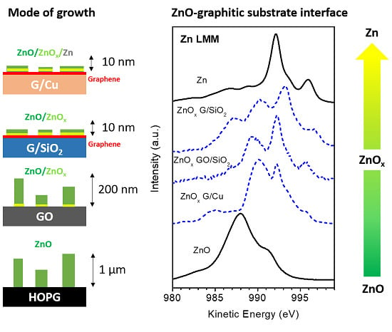
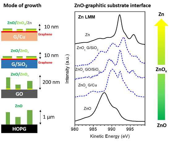
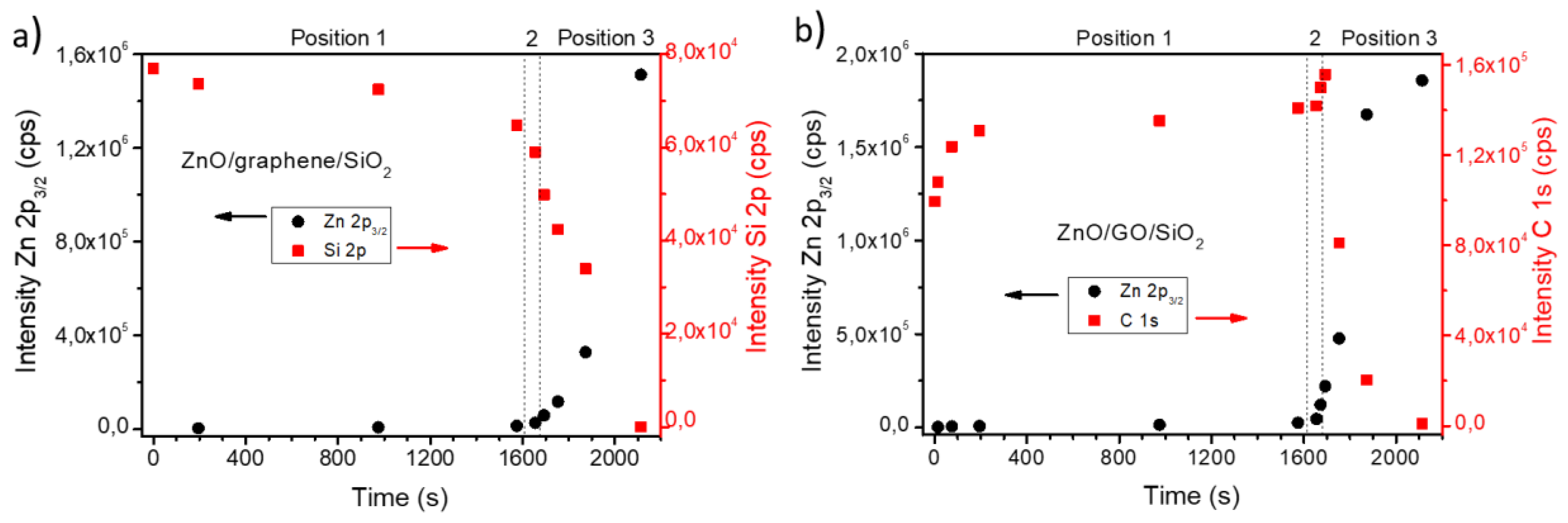
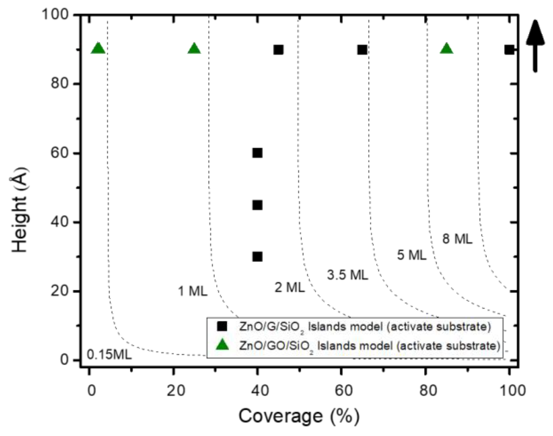
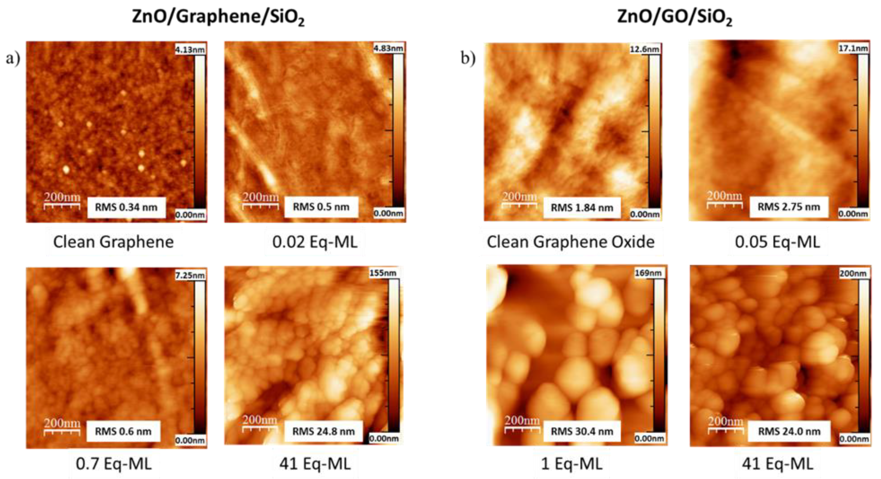
3.1. Quantitative and Morphological Analysis: ZnO Growth Mode

The first part of our study focused on the comparison of the mode of growth of ZnO on both substrates. In this regard, Figure 1 presents a common quantitative analysis of the deposition using the XPS intensity from the grown layer and the substrates, i.e., the Zn 2p 3/2 peak from ZnO and the Si 2p and C 1s XPS peaks for G/SiO2 and GO/SiO2 substrates, respectively. The coverage of ZnO in terms of equivalent monolayers (Eq-ML), assuming uniform deposition, can be estimated in each stage of growth from the measured intensities by the expression I = I 0 ( 1 e D t / λ ) . In our case, in this equation, I is the intensity of the Zn 2p contribution at each evaporation stage, I 0 is the intensity of a bulk sample of the material, t is the total evaporation time, D is the deposition rate and λ is the inelastic electron mean free path. In particular, the IMFP λ is set at 7.5 Å for the Zn 2p photoemitted electrons through the ZnO matrix, while the thickness of a ZnO monolayer is ~2.6 Å. Nevertheless, it is worth pointing out that this total coverage calculated by XPS can induce important underestimations of the total amount of deposited material depending on the characteristics of the mode of growth due to the surface nature of the photoelectrons recorded by this spectroscopic technique. By this reason, plots such as those represented in Figure 1 should be extended with further data from complementary techniques, although they give valuable qualitative information on the growth process. Figure 1a,b show the intensity of the above-mentioned XPS contributions as a function of the evaporation time on both substrates. As can be seen, the expected increase of the Zn 2p intensity in both substrates corresponds to an exponential growth mechanism (see black circles), although the growth rate for each of the three evaporation positions (see Figure S1, Supplementary Materials) is different, increasing as the sample is closer to the ZnO source. For each position, the growth was characterized by a fast deposition followed by a saturation stage of the XPS signal, indicating that (1) no more surface is covered and (2) the ZnO structures is at least as large as the IMFP of photoelectrons. For the third position, where the sample was directly facing the evaporator, the deposition, as expected, is much faster. In turn, the intensities from the substrates follows the opposite behavior (red squares). In the case of G/SiO2 the intensity of the Si 2p signal decreases with the evaporation time until it completely disappears; however, for GO, the intensity of the C 1s contribution initially increased but does not take up the expected decreasing behavior until an advanced stage of the ZnO growth at the third position. This effect will be explained below in Section 3.2 as due to reduction of GO under X-ray irradiation, releasing oxygen-based functional groups of the GO surface, thus increasing the signal from carbon atoms. Therefore, morphological but also chemical information at the qualitative level could be inferred from these simple plots.
XPS measurements can also provide deeper insights the details of the growth mode by analyzing the inelastic background (inelastic peak shape analysis (IPSA)). In this case, the probing depth was extended to several times the IMFP, as this background contains electrons that have lost part of their energy by inelastic processes that depend, among other factors, on the spatial distribution of the atoms that contribute to the signal (to the emission or/and to the inelastic scattering). Therefore, this analytical method gives the opportunity to derive the surface morphology that gives rise to the shape of the inelastic background. This method has been included in the QUASES software [46]. The survey XPS spectra for different stages of growth on both substrates were analyzed in terms of islands model (active substrate), and the results are depicted in Figure 2. For the G/SiO2 substrate (black squares), this study could not be performed for the spectra recorded at position 1, since the signal-noise ratio was very low due to the small amount of deposited material. Nevertheless, this fact would indicate that in the early stages of growth, the nucleation limits the surface coverage. Once the sample is located at position 2, the growth is characterized by a fast coverage of the surface (up to a 40%) with islands growing from 30 to 60 Å. These structures are too thick for a surface sensitive technique such as XPS (30 Å is more than three times the ZnO estimated IMFP) and would explain the limited increase on the XPS intensity, even for such big clusters. For subsequent depositions at position 3, the coverage increases until the coalescence and the height of these structures saturates at 90 Å, which is close to the limit of the IPSA method, taking into account the current IMFPs (further tuning to higher height values does not translate into background changes). For the GO substrate (green triangles), the mode of growth is simpler, characterized by a very slow nucleation process and by the growth of big clusters. Even for the early stages of growth, the height of ZnO structures reaches the maximum (90 Å). This means that the XPS intensity measured in Figure 1b is limited and controlled by the percentage of surface coverage.
The AFM topography images for different stages of growth of ZnO on G/SiO2 and GO/SiO2 are shown in Figure 3a,b, respectively. The first images of each panel correspond to the clean substrates. In the graphene case, the SiO2 support can be seen underneath and some further images show the characteristic graphene wrinkles. Although ZnO deposits can hardly be observed in the AFM images due to the small amount of deposited material (especially during the very first steps), some slight changes on the contrast appears. In particular, the root mean square (RMS) increased with the deposition time and serves as a good indicator of the deposition. However, for deposition of 0.7 Eq-ML, the AFM image clearly shows the formation of small ZnO islands with lateral size of 30–50 nm and few nanometers high, which gradually increased in size and height until the last stage, when the entire surface is covered. For the GO, the initial substrate already shows higher values of RMS than as-transferred graphene. However, similarly to the previous substrate, the ZnO grains were observed for deposits around 1 Eq-ML (calculated by XPS). As expected from IPSA analysis, the grains were bigger in size, with diameters around 200 nm and heights close to 90 nm. Therefore, the ZnO growth on graphene appeared to be smoother than on GO in the very early stages of growth, even though for larger deposits near to the coalescence of the RMS values became similar (see complete evolution of the RMS roughness for both substrates in Figure S2).
It is known that AFM images of the phase channel (or the excitation frequency when a secondary feedback loop is applied to the phase) certainly show a contrast that directly can be attributed to the chemical changes at the surface. For this reason, we present in Figure S3 the phase AFM images of the same samples shown in Figure 3. The images taken in phase mode confirms the results already observed at the topographic images.
Summarizing the above results, we could establish a detailed description and comparison of the mode of growth of ZnO on both substrates. In both cases, the growth of ZnO follows a Volmer–Weber mode, characterized by an initial stage controlled by nucleation process and a fast growth of ZnO clusters that finally coalesce, forming a microstructured film. However, there are some differences between both substrates. For G/SiO2, the nucleation process is faster and with a higher density of nucleation centers than for GO. In fact, this limits the size and height of the initial ZnO islands. In this sense, clusters do not start growing until almost half of the total surface is covered. On the contrary, nucleation at GO/SiO2 is slow and punctual with lower density of nucleation centers, allowing ZnO clusters to reach larger dimensions. These differences in the growth can be seen as the first sign of possible influence of the graphene oxidation state on the ZnO/substrate interaction.

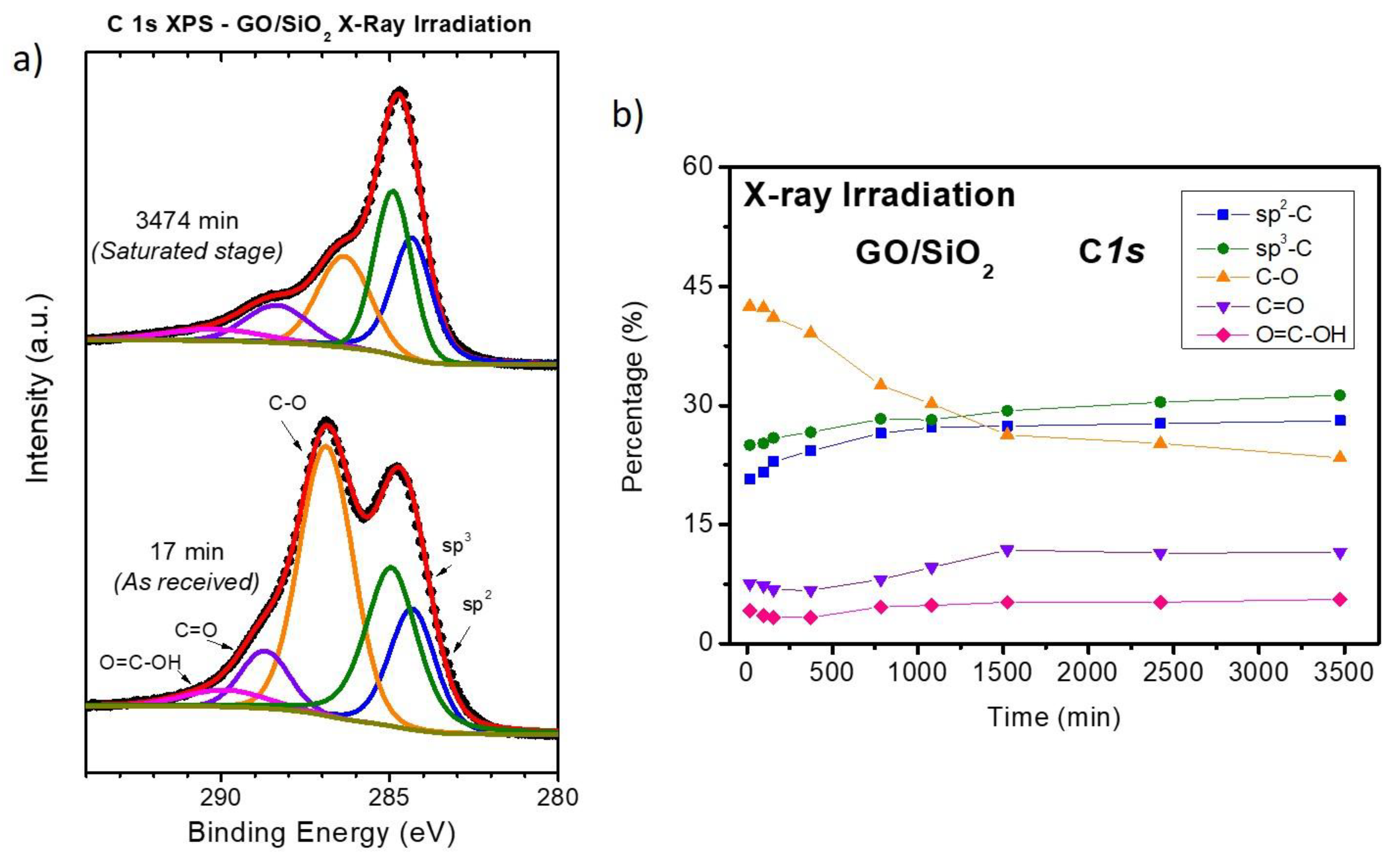
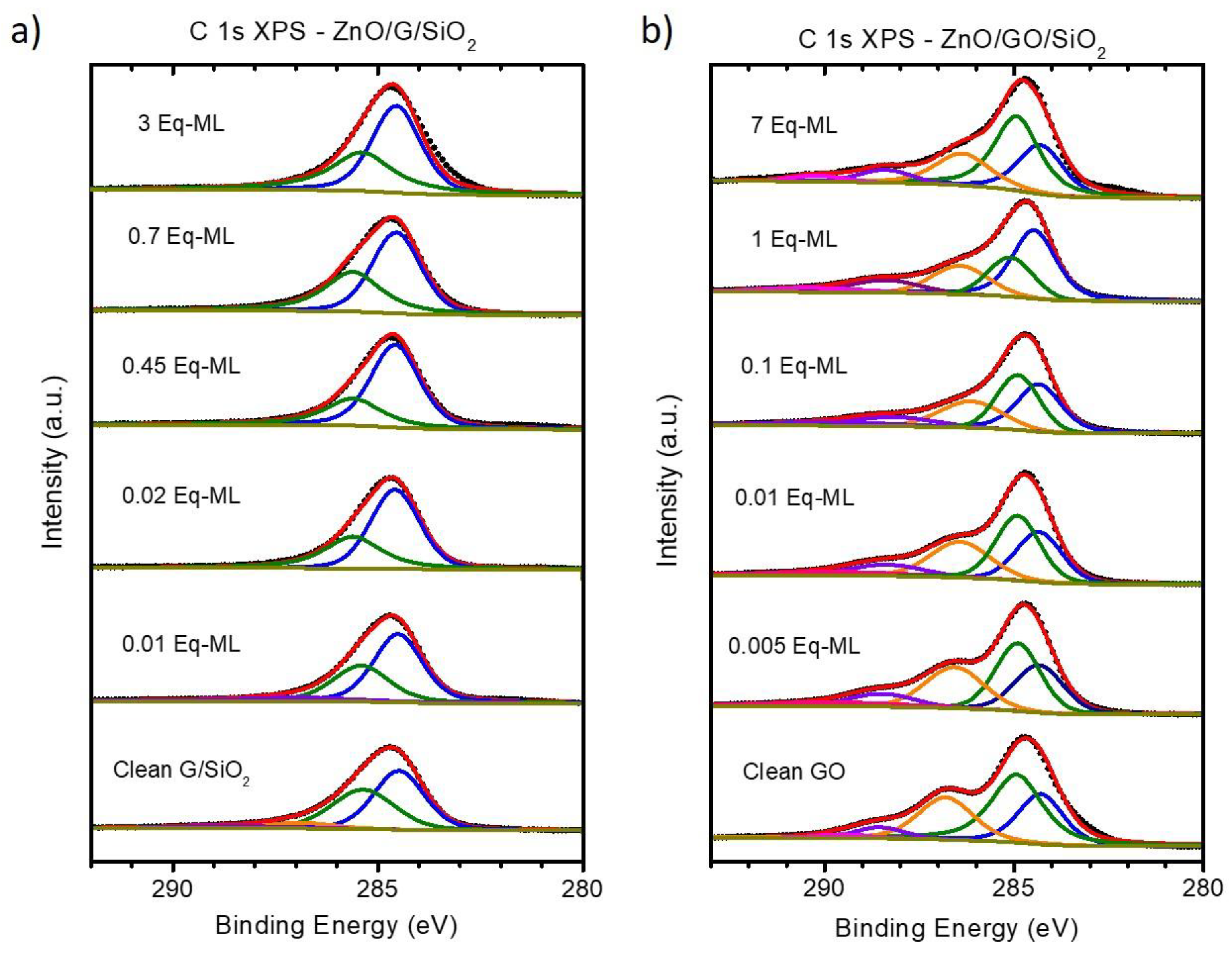
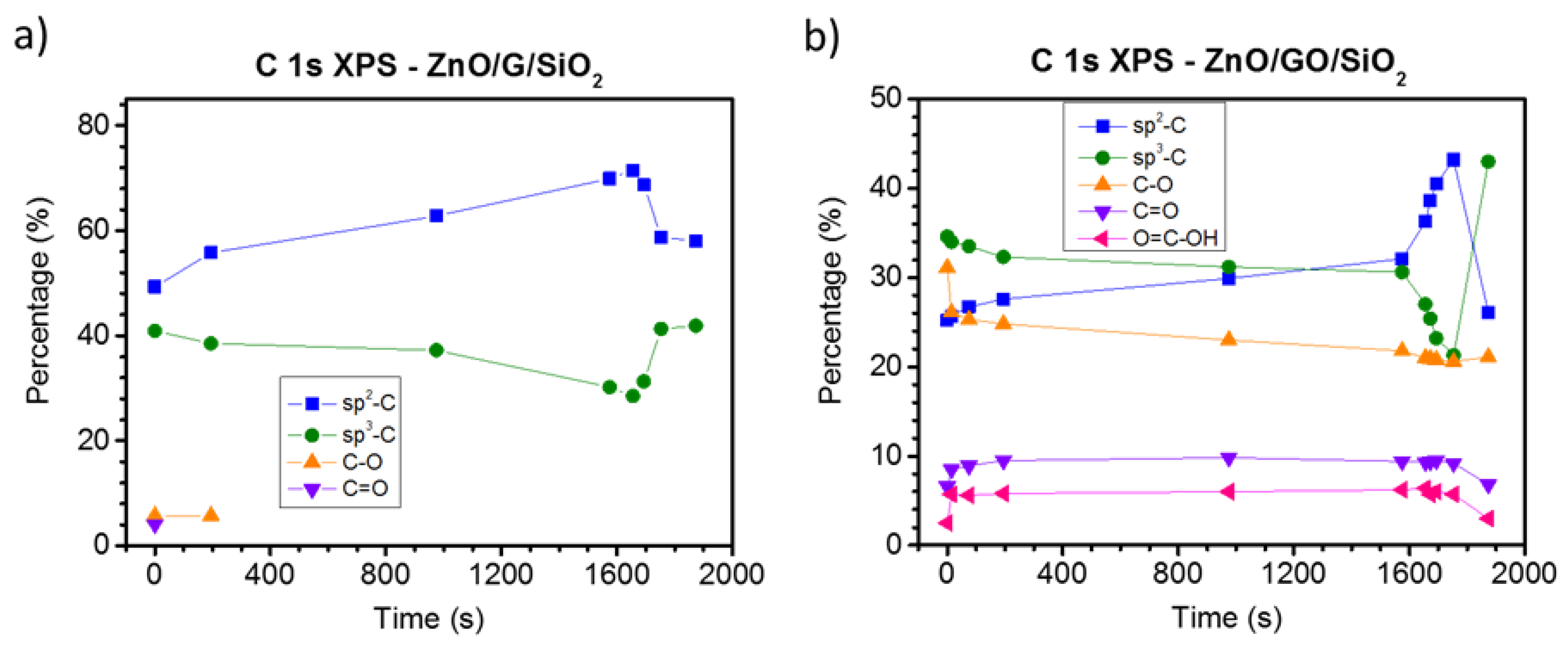
3.2. Chemical Analysis: The Interaction of ZnO with Graphene and GO

This section will focus on the chemical interaction of the substrates with the deposited ZnO and the relationship between them. Firstly, we assess the chemical damage imposed on the substrates due to the applied characterization techniques, isolating and discarding them to clearly identify the changes induced directly by the deposited ZnO. As previously stated, two main characterization techniques have been used: XPS and AFM. Regarding the last one, the non-contact tapping mode guarantees a very low interaction between sample and the cantilever tip. Moreover, these measurements were taken ex-situ, after the chemical characterization with XPS was performed. On the contrary, in-situ XPS measurements imply X-ray irradiation of the sample. It is well known that X-rays can induce changes in the oxidation state (reduction processes) [48,49] and especially degradation of organic compounds [50,51,52], depending on photon energy and flux. In particular, whereas graphene has been reported to remain stable under X-ray irradiation in the literature, GO has shown a significant reduction with time, loosing functional groups and becoming rGO under long time exposure [53,54]. It was pointed out previously that the intensity of the C 1s peak in Figure 1b increases with time, despite of ZnO deposition, suggesting a reduction induced by the X-ray flux.
In order to confirm the reduction of GO by X-ray irradiation and to differentiate it from possible changes induced by ZnO deposition, an in-situ XPS study is performed on a clean GO sample as a function of X-ray irradiation time. Focused on the C 1s XPS spectra, Figure 4a presents the XPS fitting of two spectra. The bottom spectrum shows the as received GO sample after 17 min of X-ray irradiation (which is the time it takes a complete measurement with a good signal-to-noise ratio). As it can be seen, the main peak is situated at ~287.0 eV, corresponding to single bond C–O contribution. Moreover, the spectrum also shows, with lower intensity, other peaks corresponding to double bond C=O and carboxyl groups (C(=O)OH) located at 288.7 and 290 eV, respectively [55,56]. The C–O contribution has a relative higher weight compared to sp3 [57] (originating from broken carbon hexagons on defective and messy graphitic systems) and sp2 [58] hybridization contributions at 284.7 and 284.3 eV, respectively, being both typical for graphitic compounds. The combination of all these contributions give a typical spectrum shape for the C 1s of GO. However, after ~3475 min of X-ray irradiation, oxygen is released, and the sample reaches a saturated-reduced final state. Now, the C–O contribution decreases in intensity and the sp3 peak dominates the spectrum, whereas the other carbon–oxygen components remain almost unchanged. In fact, the shape of this spectrum is much closer to the typical one for reduced GO [53,54]. Figure 4b shows the evolution with time of the relative weight of the five C 1s contributions. It can be appreciated that during the first 1500 min GO is partially reduced. As reported previously in the literature [54], the C–O component is the most affected, only partially compensated by a slight increase of the C=O and carboxylic peaks. However, both sp2 and sp3 components, keeping almost the same relative ratio during the whole time, shows an important intensity increase. For more details, see the raw C 1s and O 1s spectra as a function of time in Figure S4 of the supplementary information. Going back to the XPS characterization of the in-situ ZnO growth, the time required to measure all the regions of interest for each stage was about 3–5 h, depending on the amount of deposited material. This means that 1500 min of irradiation (about 25 h of measurements) is approximately the time needed to complete the characterization of six different stages, which was precisely the time invested to characterize the very early stages of growth. To avoid mutual interaction between this effect and those possibly provoked by ZnO deposition, we have first irradiated the GO samples for 1500 min and then performed the successive ZnO evaporations. However, this did not completely eliminate the irradiation effect. As shown in Figure 1b, for the early stages, an increase on the C 1s peak can be clearly seen, in spite of ZnO deposition. In addition, XPS is not able to measure the ZnO/GO interface (where a reduction of the GO could occur), due to the large size of the ZnO clusters, thus only the C 1s XPS signal coming from the free GO surface is measured. Therefore, the increment in C 1s intensity during the early stages of growth is related only to X-ray irradiation. Nevertheless, we would like to remark that reduction of GO promoted by irradiation during ZnO deposition occurs at a slow rate, as documented by the slow decrease in the second part of Figure 4b, from 1500 to 3500 min.
Figure 5 shows the C 1s XPS fitted spectra for a selected set of stages. On the one hand, G/SiO2 shows limited changes (see Figure 5a). Two main contributions related to sp3 and sp2 at ~285.3 and ~284.3 eV, respectively, are found for all spectra. Taking a closer look at the initial G/SiO2 clean substrate, the sp3 peak has an important relative weight, almost 40% of the total intensity. Besides, as Figure 6a shows, there is a weak contribution (<10%) from single and double bond carbon–oxygen species. As previously noted, sp3 hybridization is typically related to defects on graphitic substrates. Recalling the substrate preparation, graphene was grown on Cu sheets by CVD and then transferred to SiO2 substrates by PMMA. This route is known to induce defects on graphene and to deposit organic residues [59], increasing, broadening and shifting to higher binding energies the sp3 contribution compared to the as-received G/Cu samples previously measured by our group [41]. Interestingly, the sp2/sp3 ratio increases for the very early stages of growth as ZnO is deposited, precisely when nucleation processes are prevalent. This could indicate a preferred nucleation of ZnO clusters on these defects. Only when coalescence is almost complete a slight increase of the defect intensity is observed, in agreement with previous reported results for ZnO on G/Cu and HOPG [39,41] and other metal oxides such as CoO on HOPG [60]. On the other hand, the C 1s spectrum of the clean GO substrate shows significant differences with respect to the graphene/SiO2 substrate (see Figure 5b). Figure 6b shows that the substrate is gradually reduced upon ZnO deposition, with significant loss of C–O species (with variations limited to 10%), whereas C=O and carboxylic species slightly decrease. We attribute this change to an effect of the X-ray irradiation. The nucleation process on the defects (point/areas dominated by sp3) was in this case more pronounced than for the graphene substrate. The relative weight of the sp2 peak increases from 25 to 45%, with a similar decrease of the sp3 peak (35 to 20%). This fact could explain the differences observed during the very early stages of growth between both types of substrates, where nucleation of big ZnO clusters on the GO substrate took place from the first moment. Only for the final stages, the number of defects increases again due to the perturbing effect of ZnO on its perimeter. Moreover, we believe that the relative decrease of all carbon–oxygen species at this last stage discards the possibility of having measured traces of adsorbed COx molecules from the residual atmosphere of the vacuum chambers.
We would like to highlight that because of the type of mode of growth of ZnO/GO forming high ZnO clusters, it is not possible to achieve chemical information of the chemical state of the substrate located under the ZnO structures by XPS. However, in an indirect manner we are able to describe in detail how the initial nucleation step took place on the defects. Moreover, Raman measurements confirms that graphene is not altered by ZnO deposition at advanced stages (3Eq-ML). Figure S5 shows the Raman spectra of G/SiO2 substrates before and after ZnO deposition. The absence of the D band indicates that no defects are developed on the graphene structure, being unaltered by the ZnO deposition. GO substrates could not be measured without modification due to the high laser power.
Now we will focus on the chemical analysis of the deposited ZnO. Contrary to other transition metal oxides, the complete Zn 3d orbitals block the appearance of complex and intense shake-up contributions in the Zn 2p region [61]. Nevertheless, the Auger L3M45M45 transitions involve both Zn 2p and Zn 3d orbitals, and as long as Zn 3d states partially participate in the bonds of the compound [62,63], these Auger transitions will be sensitive to the chemical environment and, thus, to the oxidation state of Zn atoms [64]. Figure 7 shows the Auger Zn-LMM spectra of both deposits as a function of the coverage. At first glance, the growth on both substrates presents important differences. Regarding the G/SiO2 substrate, Figure 7a shows a complex shape of the spectra that results from a simple mixture of ZnO and metallic Zn reference spectra. A typical ZnO spectrum is characterized by a maximum peak at a kinetic energy (K.E.) of ~998 eV with a shoulder at higher energy, whereas metallic Zn shows a double sharper structure with energy positions of ~992 and ~995 eV (once the background is subtracted, see Figure 8b,e). However, the Zn-LMM spectra measured at the early stages of growth showed three more contributions (as shoulders) at ~990, ~994 and ~997 eV (green arrows in addition to ZnO (red arrows) and Zn (black arrows) contributions. These extra components gradually disappeared until the final shape for large coverages, corresponding to ZnO oxide. On the other hand, the growth on GO is much simpler, showing almost the same spectral shape for all deposition steps corresponding to ZnO (see Figure 7b).
In order to estimate the amount of each of these components, we have applied factor analysis (FA) with the Target Testing procedure of the reference spectra after subtraction of a Tougaard background [65]. This statistical analysis technique has been used previously by us to study the ZnO/Zn composition of the ZnO deposits on HOPG and G/Cu [39]. In that case, the ZnO growth on G/Cu substrates showed a mixture of three components: ZnO, metallic Zn and a sub-oxide, ZnOx, this last being characterized by a main peak at ~990.5 eV and two secondary contributions at ~992.5 and ~996 eV. This extra component was also confirmed by studying the XPS Zn 3d spectra. At first glance, Figure 7a recalls the extra component described above, thus we have used three initial components in the Target Testing procedure: reference ZnO and Zn spectra as well as the ZnOx spectra estimated from the G/Cu substrate.
Figure 8 shows the results of this analysis for ZnO/G/SiO2 (top) and ZnO/GO (bottom). Firstly, Figure 8a,d depict the experimental (black dots) and calculated (red lines) spectra for all analyzed stages of growth (same as those shown in Figure 7), showing very good agreement. Besides, Figure 8b,e show the final calculated reference spectra (red lines), which also agrees with the experimental ZnO and Zn contributions (black dots). However, the third component (depicted as a green dashed line) is different for both systems. For the case of ZnO/G/SiO2 it is composed of three peaks at 990 eV, 993.5 eV and 997 eV, where the two first were the most intense. Furthermore, the component that seems halfway between ZnO and Zn contributions is not an artefact, as other zinc regions, as Zn 2p, does not show a similar splitting (see Figure S6). Figure 8c shows the relative weight of ZnO, Zn and ZnOx components, i.e., the composition of the deposit) as a function of the coverage. As it can be seen, the metallic contribution is almost negligible and is noticeable only at the very beginning when the amount of sub-oxide is comparable to that of ZnO. On the other hand, the deposit on GO shows a more uniform composition. In this case, the ZnOx component maintains a contribution around 990 eV, but it also has two components overlapping in shape and energy with those of metallic Zn. It is important to remember that FA is a statistical method that can induce to non-physical solutions. Considering Figure 8f, ZnO dominates over the entire growth with >90%, only being below that value for the very early stages of growth. Precisely, is in those stages where the background removal and the signal-noise ratio can induce larger errors. Therefore, as Zn and ZnOx components are going to be present in a small proportion, it is possible that the method underestimates the presence of Zn by including that component directly on the sub-oxide component (with the 992 and 995 eV peaks). Nevertheless, the extra peak at 990 eV is not discarded.

4. Discussion

In spite of the similar chemical composition of the ZnO deposits grown on G/Cu, G/SiO2 and GO (i.e., mixture of different amounts of ZnO, Zn and ZnOx with a final predominance of the oxide), there are some clear differences, especially for the early stages of growth. Figure 9a shows from bottom to top the Zn-LMM Auger spectra of stoichiometric ZnO, ZnOx sub-oxide, related to G/Cu, G/SiO2 and GO, and metallic Zn, where G/Cu data have been taken from [39]. As described above, the three ZnOx components show similar shapes, but the relative intensities of the ~990 eV and ~993 eV Auger structures are different. The first one dominates on G/Cu and GO (as previously argued, this is the one that has physical meaning for GO case), whereas for G/SiO2 the second one gains in intensity. Figure 9b shows the Wagner plot for Zn atoms in different compounds [66], which is a very powerful tool to study initial and final states of compounds. The values marked as red solid circles have been obtained from the Zn-LMM Auger spectra measured by us from ZnO and Zn reference samples, whereas the values marked as green solid circles correspond to each of the ZnOx sub-oxide spectra above described. Other Wagner values for different zinc compounds from the literature are marked as black squares. The Wagner plot consists in depicting the K.E. of the Auger transition ( E k F ) as a function of the binding energy (B.E.) of the corresponding photoemission peak ( E b F ) . From this representation, information from initial and final states can be obtained. On the one hand, the Auger parameter is defined as α = E k F ( L 3 M 45 M 45 ) + E b F ( L 3 ) although, as shown elsewhere [65,67], this expression can be set as α = c t e L 3 M 45 M 45 + 2   R ( L 3 ) , where c t e L 3 M 45 M 45 is a constant for each element and R ( L 3 ) is the relaxation energy of the core level L3. Thus, straight lines with slope + 1 in the Wagner plot will correspond to compounds of that specific element with the same relaxation energy, i.e., same final state. Moreover, it has been also shown that E k F = c t e L 3 M 45 M 45 + [ 2 ( E M q + Φ ) 2 K Q ] 3 E b F , where the term [ 2 ( E M q + Φ ) 2 K Q ] is related to initial states. Accordingly, straight lines with slope +3 in the Wagner plot correspond to atoms with the same initial states. It is true that this simplified picture is only valid for core levels, which contrast with the fact that Zn 3d orbitals participate on the valence band. However, their hybridization is limited to a 10% in the case of ZnO [62,63], what makes us feel confident on the fact that the previous equations remain valid for the case of Zn atoms. More details regarding this discussion can be found elsewhere [39]. Blue and red squares in the Wagner plot correspond to the areas where the ~990 eV and ~993 eV peaks of the different ZnOx may appear (pertinent blue and red arrows representing these peaks are drawn in Figure 9a). As it can be seen, in both cases the areas are close and along the line with slope +3, corresponding to the same initial state than metallic Zn. This could be explained by an oxidation state lower than +2 expected for a Zn sub-oxide. In addition, the peak at ~990 eV shows a relaxation energy between metallic Zn and ZnO. The relaxation energy R ( L 3 ) is composed by three terms: R ( L 3 ) = R a t o m ( L 3 ) + R a t o m ( Q + Δ Q ) + R ( e x t r a a t o m i c ) , where R a t o m ( L 3 ) is related to the reconfiguration of the Zn electrons, R a t o m ( Q + Δ Q ) refers to the relaxation energy of the electrons transferred to the valence band from the nearby atoms and finally R ( e x t r a a t o m i c ) is the relaxation energy related to the dipoles induced in the surroundings by charge transference. As R a t o m ( L 3 ) is constant for all Zn compounds, the differences of the Auger parameter, and thus on the relaxation energy, between two Zn-LMM contributions, is given by Δ α = 2   Δ R á t o m o ( Q + Δ Q ) + 2 Δ ( e x t r a a t o m i c ) . From this expression, the variation of the Auger parameter of ZnOx and Zn would be established by differences of charge transfer from the Zn environment to screen the hole created by the emitted electron. In particular, as suggested previously [39], this could be related to charge transfer from Zn atoms, where oxygen is not able to strongly bond and the ionic character of the sub-oxide decreases compared to ZnO, reducing the extra-atomic term.
Finally, it is interesting to discuss the role of different graphitic substrates on the ZnO deposition process. HOPG and GO, which can be understood as graphene-based multilayer systems, show a similar mode of growth based in a very low rate nucleation process that leaves large non-covered areas, which translates into the growth of micrometric ZnO clusters with a composition near to stoichiometric ZnO, even for the very early stages of growth. Although it is true that GO is partially reduced when ZnO is deposited, the C 1s spectra of both substrates show clear chemical differences in terms of number of defects and oxidation state of carbon. In fact, compared to HOPG, ZnO grown on GO shows a non-negligible amount of sub-oxide, which can be only explained in terms of these initial chemical differences. Moreover, G/Cu and G/SiO2 substrates have in common that, on average, only one layer of graphene interacts with the ZnO deposits, i.e., they are graphene-monolayer-based systems. For both graphene substrates, although the mode of growth is of Volmer–Weber type, as for HOPG and GO substrates, the nucleation step is performed in different way. Now nucleation is slightly faster, especially from a certain stage, and leads to a quick coverage of a fraction of the surface with smaller ZnO structures. Precisely, it is in these early stages of growth where we found the maximum amount of this sub-oxide. Once these ZnO structures grow and the coverage continues until the coalescence, the XPS signal from this sub-oxide decreases and finally disappears, showing that it appears near the interface with the graphene substrate, whatever the support is. The chemical interaction between deposited zinc, oxygen molecules of the chamber atmosphere, graphene and support (Cu or SiO2) is extremely complex. It depends on the nature of the substrate supporting the graphene, the quality of this one and the environmental history of the sample (in terms of details of CVD process, transport and exposure to air). These cross-relations have been shown in detail for the G/Cu case [41] and will have a significant impact on the grade and characteristics of the sub-oxide, i.e., on its unique spectral shape. It is not the aim of this article to discuss in such detail the origin of this sub-oxide component for the G/SiO2 system, but to show the influence the oxidation state and number of defects of the graphitic-based substrate. In this sense, we would like to note three important points. Firstly, despite the equivalent first atomic layer of HOPG, G/SiO2 and G/Cu, the substrate below the graphene layer influences the mode of growth and chemical state of the ZnO deposit. In this sense, we point out the differences between G/Cu and G/SiO2 regarding the details of the Zn-LMM Auger transitions at the very early stages of growth. More inert substrates such as HOPG show only the deposition of ZnO, possibly related to the absence of initial reactive chemical species intercalated between the first graphene layers (as oxygen or water in the case of Cu or SiO2). More in detail, the electronic interaction between the top graphene-like layer and its support (Cu, SiO2 or even HOPG bulk) could have a significant influence on the doping of graphene, and thus possibly on its chemistry during the oxide growth. We remark that these are very complex interactions, as it was previously shown in the case of the ZnO/graphene/Cu system [40,41]. In second place both, the number of defects and different oxidation state of carbon affect also the mode of growth of ZnO, as shown by the differences between GO and the G/SiO2. Finally, and related to the first point, the growth of ZnO on multilayer graphene-based systems is different from monolayer ones, being the early stages of growth limited by a slow nucleation process.

5. Conclusions

It has been shown how the initial chemical nature of the graphene-based substrates determines the growth of ZnO performed under equivalent experimental conditions. By comparing graphene transferred to SiO2 (an inert supporting substrate that guarantees a graphene decoupled state) and GO, it is clear that the details of the mode of growth are different. Although the growth of ZnO follows a Volmer–Weber mode on both systems, the nucleation process, and thus the final size of the ZnO clusters, is different. In particular, GO shows a lower nucleation density with larger structures. B, the defects (sites with sp3 hybridization) act as nucleation sites in both cases. In addition, the interaction between deposited Zn, oxygen atmosphere and the substrates evolve in different ways. In the case of G/SiO2, an important amount of ZnOx (sub-oxide) coexists with ZnO at the very early stages of growth, the former appearing only near the ZnO/G/SiO2 interface. Although GO is partially reduced by X-ray irradiation, the difference between the oxidation state of carbon atoms is still important, as it has been proved its influence on ZnO growth. Finally, when these results are compared to similar studies regarding HOPG and G/Cu, we see more clearly how, in spite of the equivalent first atomic layer (a single plane of hexagonally coordinated carbon atoms), the characteristics of the mode of growth and the initial chemical composition of the oxide deposit are different. Therefore, the growth of metal oxides on graphene-based systems is a complex issue controlled by multiple factors such as number of defects, oxidation state, number of graphene layers (multi or monolayer systems) and complex interactions between ZnO, graphene, support (i.e., Cu or SiO2) and environmental history of the sample (for example, chemical species intercalated between graphene and support).

Supplementary Materials

The following are available online at https://0-www-mdpi-com.brum.beds.ac.uk/2311-5629/6/2/41/s1.

Author Contributions

M.A.G.-A.: data curation, formal analysis, writing—original draft; C.M.: data curation, formal analysis, writing—original draft; J.M.: data curation, formal analysis; A.d.C.: data curation, formal analysis; F.J.U.: formal analysis; A.D.: formal analysis; L.R.: formal Analysis; J.I.F.: formal Analysis; D.G.: formal analysis; L.S.: funding acquisition, supervision, writing—review and editing. All authors have read and agreed to the published version of the manuscript.

Funding

This investigation has been funded by the MINECO of Spain through the FIS2015-67367-C2-1-P project and by the Comunidad de Madrid through the NANOMAGCOST-CM P2018/NMT4321 project. One of the authors (C.M.) thanks MCIU for a FPU grant.

Acknowledgments

We also want to thank SEGAINVEX-UAM and SIdI-UAM for technical support.

Conflicts of Interest

The authors declare no conflict of interest.

References

  1. Nguyen-Phan, T.D.; Pham, V.H.; Shin, E.W.; Pham, H.D.; Kim, S.; Chung, J.S.; Seung, E.J.K.; Hur, H. The role of graphene oxide content on the adsorption-enhanced photocatalysis of titanium dioxide/graphene oxide composites. Chem. Eng. J. 2011, 170, 226–232. [Google Scholar] [CrossRef]
  2. Hu, M.; Yao, Z.; Wang, X. Graphene-Based Nanomaterials for Catalysis. Ind. Eng. Chem. Res. 2017, 56, 13, 3477–3502. [Google Scholar] [CrossRef]
  3. Mahmoudi, T.; Wang, Y.; Hahn, Y.B. Graphene and its derivatives for solar cells application. Nano Energy 2018, 47, 51–65. [Google Scholar] [CrossRef]
  4. Milić, J.V.; Arora, N.; Dar, M.I.; Zakeeruddin, S.M.; Grätzel, M. Reduced Graphene Oxide as a Stabilizing Agent in Perovskite Solar Cells. Adv. Mater. Interfaces 2018, 5, 1800416. [Google Scholar] [CrossRef]
  5. Chidembo, A.; Aboutalebi, S.H.; Konstantinov, K.; Salari, M.; Winton, B.; Yamini, S.A.; Nevirkovets, I.P.; Liu, H.K. Globular reduced graphene oxide-metal oxide structures for energy storage applications. Energy Environ. Sci. 2012, 5, 5236–5240. [Google Scholar] [CrossRef] [Green Version]
  6. Wuab, Z.S.; Zhoua, G.; Yin, L.C.; Ren, W.; Li, F.; Cheng, H.M. Graphene/metal oxide composite electrode materials for energy storage. Nano Energy 2012, 1, 107–131. [Google Scholar] [CrossRef]
  7. Justino, C.I.L.; Gomes, A.R.; Freitas, A.C.; Duarte, A.C.; Rocha-Santos, T.A.P. Graphene based sensors and biosensors. Trac-Trend Anal. Chem. 2017, 91, 53–66. [Google Scholar] [CrossRef]
  8. Chiu, N.F.; Fan, S.Y.; Yang, C.D.; Huang, T.Y. Carboxyl-functionalized graphene oxide composites as SPR biosensors with enhanced sensitivity for immunoaffinity detection. Biosens. Bioelectron. 2017, 89, 370–376. [Google Scholar] [CrossRef]
  9. Han, T.H.; Kim, H.; Kwon, S.J.; Lee, T.W. Graphene-based flexible electronic devices. Mater. Sci. Eng. R-Rep. 2017, 118, 1–43. [Google Scholar] [CrossRef]
  10. Liang, Y.; Zhao, F.; Cheng, Z.; Deng, Y.; Xiao, Y.; Cheng, H.; Zhang, P.; Huang, Y.; Shao, H.; Qu, L. Electric power generation via asymmetric moisturizing of graphene oxide for flexible, printable and portable electronics. Energy Environ. Sci. 2018, 11, 1730–1735. [Google Scholar] [CrossRef]
  11. Edalati, K.; Shakiba, A.; Vahdati-Khaki, J.; Zebarjad, S.M. Low-temperature hydrothermal synthesis of ZnO nanorods: Effects of zinc salt concentration, various solvents and alkaline mineralizers. Mater. Res. Bull. 2016, 74, 374–379. [Google Scholar] [CrossRef]
  12. Sphanel, L.; Anderson, M.A. Semiconductor clusters in the sol-gel process: Quantized aggregation, gelation, and crystal growth in concentrated zinc oxide colloids. J. Am. Chem. Soc. 1991, 113, 2826–2833. [Google Scholar] [CrossRef]
  13. Hasnidawani, J.N.; Azlina, H.N.; Norita, H.; Bonnia, N.N.; Ratim, S.; Ali, E.S. Synthesis of ZnO Nanostructures Using Sol-Gel Method. Procedia Chem. 2016, 19, 211–216. [Google Scholar] [CrossRef] [Green Version]
  14. Lee, Y.; Kim, D.Y.; Lee, S. Low-Power Graphene/ZnO Schottky UV Photodiodes with Enhanced Lateral Schottky Barrier Homogeneity. Nanomaterials 2019, 9, 799. [Google Scholar] [CrossRef] [Green Version]
  15. Gao, W.; Li, Z. ZnO thin films produced by magnetron sputtering. Ceram. Int. 2004, 30, 1155–1159. [Google Scholar] [CrossRef]
  16. Al Asmar, R.; Zaouk, D.; Bahouth, P.; Podleki, J.; Foucaran, A. Characterization of electron beam evaporated ZnO thin films and stacking ZnO fabricated by e-beam evaporation and RF magnetron sputtering for the realization of resonators. Microelectron. Eng. 2006, 83, 393–398. [Google Scholar] [CrossRef]
  17. Özgür, Ü.; Alivov, Y.I.; Liu, C.; Teke, A.; Reshchikov, M.A.; Doğan, S.; Avrutin, V.; Cho, S.J.; Morkoç, H. A comprehensive review of ZnO materials and devices. J. Appl. Phys. 2005, 98, 041301. [Google Scholar] [CrossRef] [Green Version]
  18. Kim, H.; Gilmore, C.M.; Horwitz, J.S.; Piqué, A.; Murata, H.; Kushto, G.P.; Schlaf, R.; Kafafi, Z.H.; Chrisey, D.B. Transparent conducting aluminum-doped zinc oxide thin films for organic light-emitting devices. Appl. Phys. Lett. 2000, 76, 259. [Google Scholar] [CrossRef]
  19. Rousset, J.; Saucedo, E.; Lincot, D. Extrinsic Doping of Electrodeposited Zinc Oxide Films by Chlorine for Transparent Conductive Oxide Applications. Chem. Mater. 2009, 21, 3, 534–540. [Google Scholar] [CrossRef]
  20. Hoffman, R.L. ZnO-channel thin-film transistors: Channel mobility. J. Appl. Phys. 2004, 95, 5813. [Google Scholar] [CrossRef]
  21. Huang, J.; Wang, L.; Xu, R.; Tang, K.; Shi, W.; Xia, Y. Growth of p-type ZnO films and fabrication of ZnO photodiode-based UV detectors. Semicond. Sci. Technol. 2009, 24, 075025. [Google Scholar] [CrossRef]
  22. Sekine, N.; Chou, C.H.; Kwan, W.L.; Yang, Y. ZnO nano-ridge structure and its application in inverted polymer solar cell. Org. Electron. 2009, 10, 1473–1477. [Google Scholar] [CrossRef]
  23. Zhu, L.; Zeng, W. Room-temperature gas sensing of ZnO-based gas sensor: A review. Sens. Actuator A 2017, 267, 242–261. [Google Scholar] [CrossRef]
  24. Mattevi, C.; Kima, H.; Chhowalla, M. A review of chemical vapour deposition of graphene on copper. J. Mater. Chem. 2011, 21, 3324. [Google Scholar] [CrossRef]
  25. Chen, J.H.; Jang, C.; Xiao, S.; Ishigami, M.; Fuhrer, M.S. Intrinsic and extrinsic performance limits of graphene devices on SiO2. Nat. Nanotechnol. 2008, 3, 206–209. [Google Scholar] [CrossRef] [PubMed]
  26. Papageorgiou, D.G.; Kinloch, I.A.; Young, R.J. Mechanical properties of graphene and graphene-based nanocomposites. Prog. Mater. Sci. 2017, 90, 75–127. [Google Scholar] [CrossRef]
  27. Tavakoli, M.M.; Aashuri, H.; Simchi, A.; Fan, Z. Hybrid zinc oxide/graphene electrodes for depleted heterojunction colloidal quantum-dot solar cells. Phys. Chem. Chem. Phys. 2015, 17, 24412–24419. [Google Scholar] [CrossRef]
  28. Zhang, T.F.; Wu, G.A.; Wang, J.Z.; Yu, Y.Q.; Zhang, D.Y.; Wang, D.D.; Jiang, J.B.; Wang, J.M.; Luo, L.B. A sensitive ultraviolet light photodiode based on graphene-on-zinc oxide Schottky junction. Nanophotonics 2017, 6, 1073–1081. [Google Scholar] [CrossRef] [Green Version]
  29. Dreyer, D.R.; Park, S.; Bielawski, C.W.; Ruoff, R.S. The chemistry of graphene oxide. Chem. Soc. Rev. 2010, 39, 228–240. [Google Scholar] [CrossRef]
  30. Zhao, C.; Xing, L.; Xiang, J.; Cui, L.; Jiao, J.; Sai, H.; Li, Z.; Li, F. Formation of uniform reduced graphene oxide films on modified PET substrates using drop-casting method. Particuology 2014, 17, 66–73. [Google Scholar] [CrossRef]
  31. Puah, P.Y.; Moh, P.Y.; Lee, P.C.; How, S.E. Spin-coated graphene oxide as a biomaterial for Wharton’s Jelly derived mesenchymal stem cell growth: A preliminary study. Adv. Perform. Mater. 2018, 33, 835–843. [Google Scholar] [CrossRef]
  32. Jadhav, S.T.; Rajoba, S.J.; Patil, S.A.; Han, S.H.; Jadhav, L.D. Temperature-Dependent Photoluminescence of Graphene Oxide. J. Electron. Mater. 2016, 45, 379–385. [Google Scholar] [CrossRef]
  33. Holm, A.; Wrasman, C.J.; Kao, K.C.; Riscoe, A.R.; Cargnello, M.; Frank, C.W. Langmuir–Blodgett Deposition of Graphene Oxide—Identifying Marangoni Flow as a Process that Fundamentally Limits Deposition Control. Langmuir 2018, 34, 33, 9683–9691. [Google Scholar] [CrossRef]
  34. Jilani, S.M.; Banerji, P. Graphene Oxide−Zinc Oxide Nanocomposite as Channel Layer for Field Effect Transistors: Effect of ZnO Loading on Field Effect Transport. Appl. Mater. Interfaces 2014, 6, 16941–16948. [Google Scholar] [CrossRef]
  35. Kumar, B.; Lee, K.Y.; Park, H.K.; Chae, S.J.; Lee, Y.H.; Kim, S.W. Controlled Growth of Semiconducting Nanowire, Nanowall, and Hybrid Nanostructures on Graphene for Piezoelectric Nanogenerators. ACS Nano 2011, 5, 4197–4204. [Google Scholar] [CrossRef]
  36. Zheng, L.; Cheng, X.; Cao, D.; Wang, G.; Wang, Z.; Xu, D.; Xia, C.; Shen, L.; Yu, Y.; Shen, D. Improvement of Al2O3 Films on Graphene Grown by Atomic Layer Deposition with Pre-H2O Treatment. ACS Appl. Mater. Interfaces 2014, 6, 7014–7019. [Google Scholar] [CrossRef] [PubMed]
  37. Schilirò, E.; Nigro, R.L.; Roccaforte, F.; Deretzis, I.; La Magna, A.; Armano, A.; Agnello, S.; Pecz, B.; Ivanov, I.G.; Yakimova, R.; et al. Seed-Layer-Free Atomic Layer Deposition of Highly Uniform Al2O3 Thin Films onto Monolayer Epitaxial Graphene on Silicon Carbide. Adv. Mater. Interfaces 2019, 6, 1900097. [Google Scholar] [CrossRef]
  38. Hong, H.K.; Jo, J.; Hwang, D.; Lee, J.; Kim, N.Y.; Son, S.; Kim, J.H.; Jin, M.J.; Jun, Y.C.; Erni, R.; et al. Atomic Scale Study on Growth and Heteroepitaxy of ZnO Monolayer on Graphene. Nano Lett. 2017, 17, 120–127. [Google Scholar] [CrossRef] [Green Version]
  39. Morales, C.; Black, A.; Urbanos, F.J.; Granados, D.; Méndez, J.; del Campo, A.; Yubero, F.; Soriano, L. Study of the Interface of the Early Stages of Growth under Quasi-Equilibrium Conditions of ZnO on Graphene/Cu and Graphite. Adv. Mater. Interfaces 2019, 6, 1801689. [Google Scholar] [CrossRef]
  40. Morales, C.; Urbanos, F.J.; del Campo, A.; Leinen, D.; Granados, D.; Prieto, P.; Aballe, L.; Foerster, M.; Soriano, L. Chemical and electronic inhomogeneities of Graphene on polycrystalline Cu and its influence on the early stages of growth of ZnO. Carbon 2020. Under review. [Google Scholar]
  41. Morales, C.; Urbanos, F.J.; del Campo, A.; Leinen, D.; Granados, D.; Rodríguez, M.A.; Soriano, L. Electronic Decoupling of Graphene from Copper Induced by Deposition of ZnO: A Complex Substrate/Graphene/Deposit/Environment Interaction. Adv. Mater. Interfaces 2020, 1902062. [Google Scholar] [CrossRef]
  42. Black, A.; Jiménez, F.; Benardo-Gavito, R.; Casado, S.; Granados, D.; Vázquez de Parga, A.L. Growth and characterization of 7,7,8,8-tetracyano-quinodimethane crystals on chemical vapor deposition graphene. J. Cryst. Growth 2016, 453, 1–6. [Google Scholar] [CrossRef] [Green Version]
  43. Díaz-Fernández, D.; Méndez, J.; Yubero, F.; Domínguez-Cañizares, G.; Gutiérrez, A.; Soriano, L. Study of the early stages of growth of Co oxides on oxide substrates. Surf. Interface Anal. 2014, 46, 975–979. [Google Scholar] [CrossRef]
  44. Moulder, J.F.; Stickle, W.F.; Sobol, P.E.; Bomben, K.D.; Chastain, J. (Eds.) Handbook of X-ray Photoelectron Spectroscopy, Perkin–Elmer Corporation Physical Electronics Division; Perkin-Elmer Corporation, Physical Electronics Division: Eden Prairie, MN, USA, 1992. [Google Scholar]
  45. Tanuma, S.; Powell, C.J.; Penn, D.R. Proposed formula for electron inelastic mean free paths based on calculations for 31 materials. Surf. Sci. Lett. 1987, 192, L849–L857. [Google Scholar] [CrossRef]
  46. Touggard, S. Quases Software. Available online: www.QUASES.com (accessed on 31 July 2017).
  47. Horcas, I.; Fernández, R.; Gómez Rodríguez, J.M.; Colchero, J.; Gómez Herrero, J.; Baró, A.M. WSXM: A software for scanning probe microscopy and a tool for nanotechnology. Rev. Sci. Instrum. 2007, 78, 013705. [Google Scholar] [CrossRef]
  48. Mendialdu, J.; Casanov, R.; Barbaux, Y. XPS studies of V2O5, V6O13, VO2 and V2O3. J. Electron Spectrosc. Relat. Phenom. 1995, 71, 249–261. [Google Scholar] [CrossRef]
  49. Baer, D.R.; Engelhard, M.H.; Lea, A.S. Introduction to Surface Science Spectra data on electron and x-ray damage: Sample degradation during XPS and AES measurements. Surf. Sci. Spectra 2003, 10, 47. [Google Scholar] [CrossRef]
  50. Buchwalter, L.P.; Czornyj, G. Poly (methyl methacrylate) degradation during x-ray photoelectron spectroscopy analysis. J. Vac. Sci. Technol. A 1990, 8, 781. [Google Scholar] [CrossRef]
  51. Sato, M.; Furusawa, T.; Hotta, T.; Watanabe, H.; Suzuki, N. Effect of oxide thickness on the degradation of organic silane monolayers on silicon wafer surface during XPS measurement. Surf. Interface Anal. 2006, 38, 838–841. [Google Scholar] [CrossRef]
  52. Recek, N.; Primc, G.; Vesel, A.; Mozetic, M.; Avila, J.; Razado-Colambo, I.; Asensio, M. Degradation of Albumin on Plasma-Treated Polystyrene by Soft X-ray Exposure. Polymers 2016, 8, 244. [Google Scholar] [CrossRef] [Green Version]
  53. Blanton, T.N.; Majumdar, D. Characterization of X-ray irradiated graphene oxide coatings using X-ray diffraction, X-ray photoelectron spectroscopy, and atomic force microscopy. Powder Diffr. 2013, 28, 68–71. [Google Scholar] [CrossRef] [Green Version]
  54. Silipigni, L.; Cutroneo, M.; Salvato, G.; Torrisi, L. In-situ soft X-ray effects on graphene oxide films. Radiat. Eff. Defects Solids 2018, 173, 740–750. [Google Scholar] [CrossRef]
  55. Yang, D.; Velamakanni, A.; Bozoklu, G.; Park, S.; Stoller, M.; Piner, R.D.; Stankovich, S.; Jung, I.; Field, D.A.; Ventrice, C.A., Jr.; et al. Chemical analysis of graphene oxide films after heat and chemical treatments by X-ray photoelectron and Micro-Raman spectroscopy. Carbon 2009, 47, 145–152. [Google Scholar] [CrossRef]
  56. Haubner, K.; Murawski, J.; Olk, P.; Eng, L.M.; Ziegler, C.; Adolphi, B.; Jaehne, E. The route to functional graphene oxide. Chem. Phys. Chem. 2010, 11, 2131–2139. [Google Scholar] [CrossRef] [PubMed]
  57. Hontoria-Lucas, C.; López-Peinado, A.J.; López-González, J.D.; Rojas-Cervantes, M.L.; Martín-Aranda, R.M. Study of oxygen-containing groups in a series of graphite oxides: Physical and chemical characterization. Carbon 1995, 33, 1585–1592. [Google Scholar] [CrossRef]
  58. Webb, M.J.; Palmgren, P.; Pal, P.; Karis, O.; Grennberg, H. A simple method to produce almost perfect graphene on highly oriented pyrolytic graphite. Carbon 2011, 49, 3242–3249. [Google Scholar] [CrossRef] [Green Version]
  59. Cunge, G.; Ferrah, D.; Petit-Etienne, C.; Davydova, A.; Okuno, H.; Kalita, D.; Bouchiat, V.; Renault, O. Dry efficient cleaning of poly-methylmethacrylate residues from graphene with high-density H2 and H2-N2 plasmas. J. Appl. Phys. 2015, 118, 123302. [Google Scholar] [CrossRef]
  60. Morales, C.; Díaz-Fernández, D.; Mossanek, R.J.O.; Abbate, M.; Méndez, J.; Pérez-Dieste, V.; Escudero, C.; Rubio-Zuazo, J.; Prieto, P.; Soriano, L. Controlled ultra-thin oxidation of graphite promoted by cobalt oxides: Influence of the initial 2D CoO wetting layer. Appl. Surf. Sci. 2020, 509, 145118. [Google Scholar] [CrossRef]
  61. Rössler, N.; Kotsis, K.; Staemmler, V. Ab initio calculations for the Zn 2s and 2p core level binding energies in Zn oxo compounds and ZnO. Phys. Chem. Chem. Phys. 2006, 8, 697. [Google Scholar] [CrossRef] [PubMed]
  62. Leontiev, S.A.; Koshcheev, S.V.; Devyatov, V.G.; Cherkashin, A.E.; Mikheeva, P. Detailed XPS and UPS studies of the band structure of zinc oxide. J. Struct. Chem. 1997, 38, 725. [Google Scholar] [CrossRef]
  63. Mikheeva, P.; Zhidomirov, G.M.; Ruzankin, S.F.; Leontiev, S.A.; Devyatov, V.G.; Koshcheev, S.V.; Cherkashin, A.E. Modeling the photoelectron spectra of the valence O2p-band of zinc oxide by the Xα-scattered wave method. J. Struct. Chem. 1997, 38, 732. [Google Scholar] [CrossRef]
  64. Deroubaix, G.; Marcus, P. X-ray photoelectron spectroscopy analysis of copper and zinc oxides and sulphides. Surf. Interface Anal. 1992, 18, 39–46. [Google Scholar] [CrossRef]
  65. Aronniemi, M.; Sainio, J.; Lahtinen, J. Aspects of using the factor analysis for XPS data interpretation. Surf. Sci. 2007, 601, 479–489. [Google Scholar] [CrossRef]
  66. Measurement Services Division of the National Institute of Standards and Technology (NIST), Wagner Plot. Available online: https://srdata.nist.gov/xps/main_search_menu.aspx (accessed on 5 June 2018).
  67. Wagner, C.D.; Joshi, A. The auger parameter, its utility and advantages: A review. J. Electron Spectrosc. Relat. Phenom. 1988, 47, 283. [Google Scholar] [CrossRef]
Figure 1. XPS intensities of the Zn 2p 3/2 (dots) and Si 2p/C 1s (squares) peaks versus evaporation time for the growth of: (a) ZnO/G/SiO2 and (b) ZnO/GO/SiO2.
Carbon 06 00041 g001
Figure 2. Results for the inelastic peak shape analysis for the growth of ZnO on G/SiO2 (black squares) and GO (green triangles).
Carbon 06 00041 g002
Figure 3. AFM images (1 × 1 μm2) for different stages of growth of ZnO on (a) G/SiO2 and (b) GO/SiO2. The RMS roughness and the color scale bar for each image is given.
Carbon 06 00041 g003
Figure 4. (a) Fitted XPS C 1s spectra of as received GO/SiO2 (bottom) and GO/SiO2 after 3474 min of X-ray irradiation (top). (b) Relative intensities of the XPS C 1s contributions used for the fitting in (a) as a function of irradiation time.
Carbon 06 00041 g004
Figure 5. In-situ C 1s XPS spectra for (a) ZnO/G/SiO2 and (b) ZnO/GO/SiO2 for a selected set of deposition stages.
Carbon 06 00041 g005
Figure 6. Relative intensities of the XPS C 1s contributions used for the fitting of the spectra in Figure 5 as a function of evaporation time for ZnO on (a) G/SiO2 and (b) GO/SiO2.
Carbon 06 00041 g006
Figure 7. Auger Zn-LMM XPS spectra as a function of the coverage for the growth of: (a) ZnO/G/SiO2 and (b) ZnO/GO/SiO2. Energy positions of the main Auger peaks for ZnO (red arrows), metallic Zn (black arrows) and ZnOx (green arrows) are indicated.
Carbon 06 00041 g007
Figure 8. Results of factor analysis applied to the Zn-LMM XPS spectra for the growth of ZnO on G/SiO2 (ac) and GO (df). (a) and (d): Calculated and suggested bases used in factor analysis. (b) and (e): Fittings of the experimental spectra using a linear combination of the proposed components. (c) and (f): Concentration for each of the components as a function of the coverage.
Carbon 06 00041 g008
Figure 9. (a) Zn-LMM spectra for ZnO and Zn reference samples and calculated ZnOx contributions. (b) Wagner plot for different Zn compounds found in the literature (squares). The values obtained in this work for ZnOx are depicted as green circles. Values obtained from ZnO and Zn reference samples are depicted as red circles.
Carbon 06 00041 g009

