Article

Nitrogen-Doped Flower-Like Hybrid Structure Based on Three-Dimensional Graphene

by
Kinshuk Dasgupta
1,2,*,
Mahnoosh Khosravifar
3,
Shrilekha Sawant
4,
Paa Kwasi Adusei
3,
Sathya Narayan Kanakaraj
3,
Jacob Kasik
1 and
Vesselin Shanov
1,3,*
1
Department of Chemical and Environmental Engineering, University of Cincinnati, Cincinnati, OH 45221, USA
2
Materials Group, Bhabha Atomic Research Centre, Mumbai 400085, India
3
Department of Mechanical and Materials Engineering, University of Cincinnati, Cincinnati, OH 45221, USA
4
Department of Chemical Engineering, Institute of Chemical Technology, Mumbai 400019, India
*
Authors to whom correspondence should be addressed.
Submission received: 3 May 2020 / Revised: 12 June 2020 / Accepted: 16 June 2020 / Published: 19 June 2020
(This article belongs to the Special Issue Characterization and Standardization of Graphene Materials)

Abstract

:
A new flower-like hybrid structure consisting of nitrogen-doped 3-dimensional (3D) graphene and vertically aligned graphene has been synthesized using a combination of low-pressure chemical vapor deposition (LPCVD) and plasma-enhanced chemical vapor deposition (PECVD) techniques. Active nitrogen (N) species were found to be essential for the growth of the flower-like morphology. N-doping was responsible for enhanced electrical conductivity and wettability of the obtained nano-carbon hybrid structure. Based on the conducted studies a growth mechanism has been proposed. The high specific surface area, low resistance to charge transfer and enhanced specific capacitance of this nitrogen-doped hybrid structure, makes it an excellent candidate material for supercapacitors.

Graphical Abstract

1. Introduction

Graphene and graphene derivatives have been vigorously studied due to their unique structures and properties. The attractive properties of 2D graphene have already been translated into the 3D graphene [1,2,3,4]. In 2011, when the synthesis of graphene foam was reported with high specific surface area [1], intensive investigation started on various applications mostly on electrochemical energy storage [5,6,7,8,9,10,11,12,13,14]. With time, the poor electrical conductivity of initial graphene foams (≈1 S/cm) was overcome by modifying the catalysts and synthesis method which yielded better conductivity of ≈50 S/cm [2]. High quality 3D graphene structures are promising for sensors [15,16], field effect transistors [17], supercapacitors [18], batteries [19], photovoltaic devices [20], and electron emission applications [21]. In recent years, researchers have shown much interest in vertically aligned graphene (VG) or carbon nanowalls, which are the stacked graphene sheets standing almost vertically to the substrate [22]. Due to its architecture comprising sharp edges and high surface to volume ratio, this material reveals great potential in biosensing, energy storage, and electron emission applications [23,24,25]. There have been reports of various morphologies of VG, such as turnstile-like [26], maze-like [27], and petal-like [28,29].
Hybrid structures comprising horizontal and vertical nanostructures of carbon are of greater interest because they can provide more specific surface area, structural stability, and tailored functionality compared to the individual one. So far, the growth of carbon nanotube (CNT) on graphene or vice versa has been reported. Choi et al. [30] have described the one-step growth of graphene on the tips of CNTs. Zhang et al. [31] reported the growth of mushroom gills-like graphene flakes on top of CNT arrays. Further, Zhao et al. [32], Kim et al. [33], and Wu et al. [34] have demonstrated the growth of CNT over graphene. Harris et al. [35] have discussed the structure of junctions between CNT and graphene. 3D graphene-CNT hybrid has been developed in the form of aerogel for use in Li-Se battery [36]. To the best of our knowledge, no reports have been found related to the growth of a hybrid structure consisting of VG on 3D graphene.
Nitrogen (N) doping in carbon nanostructures is considered to improve their performance [37]. Enhancement of capacitance, sensing efficiency, and chemical activity in graphene has been reported by various researchers [38,39,40]. Introduction of nitrogen (or ammonia) in the synthesis atmosphere not only dopes N into the graphitic lattice but also increases the growth rate of the product [24].
The objective of the present work is to grow an N doped hybrid structure comprising 3D graphene and vertically oriented graphene (VG) having superior properties than that of 3D graphene alone. Our group developed earlier a process of catalyst preparation using Ni powder and polymer to synthesize 3D graphene [2]. In the present work, a slight modification of that process has been carried out in order to obtain a Ni framework. Using this framework, initially, N doped 3D graphene was grown using LPCVD. Further, employing the same catalyst N doped graphene with flower-like morphology was grown over N doped 3D graphene using plasma-enhanced chemical vapor deposition (PECVD) in the same reactor. The electric fields associated with plasma are believed to play a significant role in the vertical growth of carbon nanostructures [5,41]. They help in aligning the graphene along the direction of the field. Moreover, PECVD is advantageous in terms of enabling a low synthesis temperature and efficient doping due to presence of various active species. This novel hybrid structure revealed higher specific surface area and better electrochemical properties compared to 3D graphene making it a suitable material for supercapacitors and other advanced applications.

2. Materials and Methods

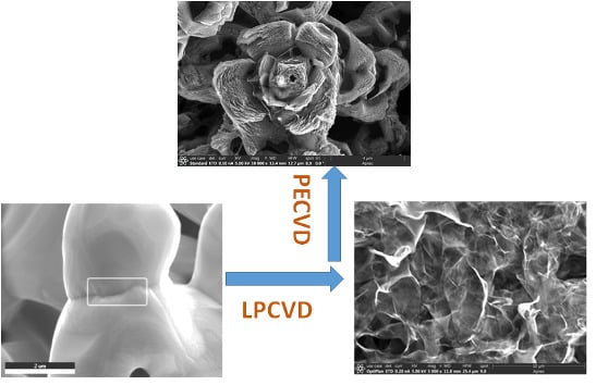
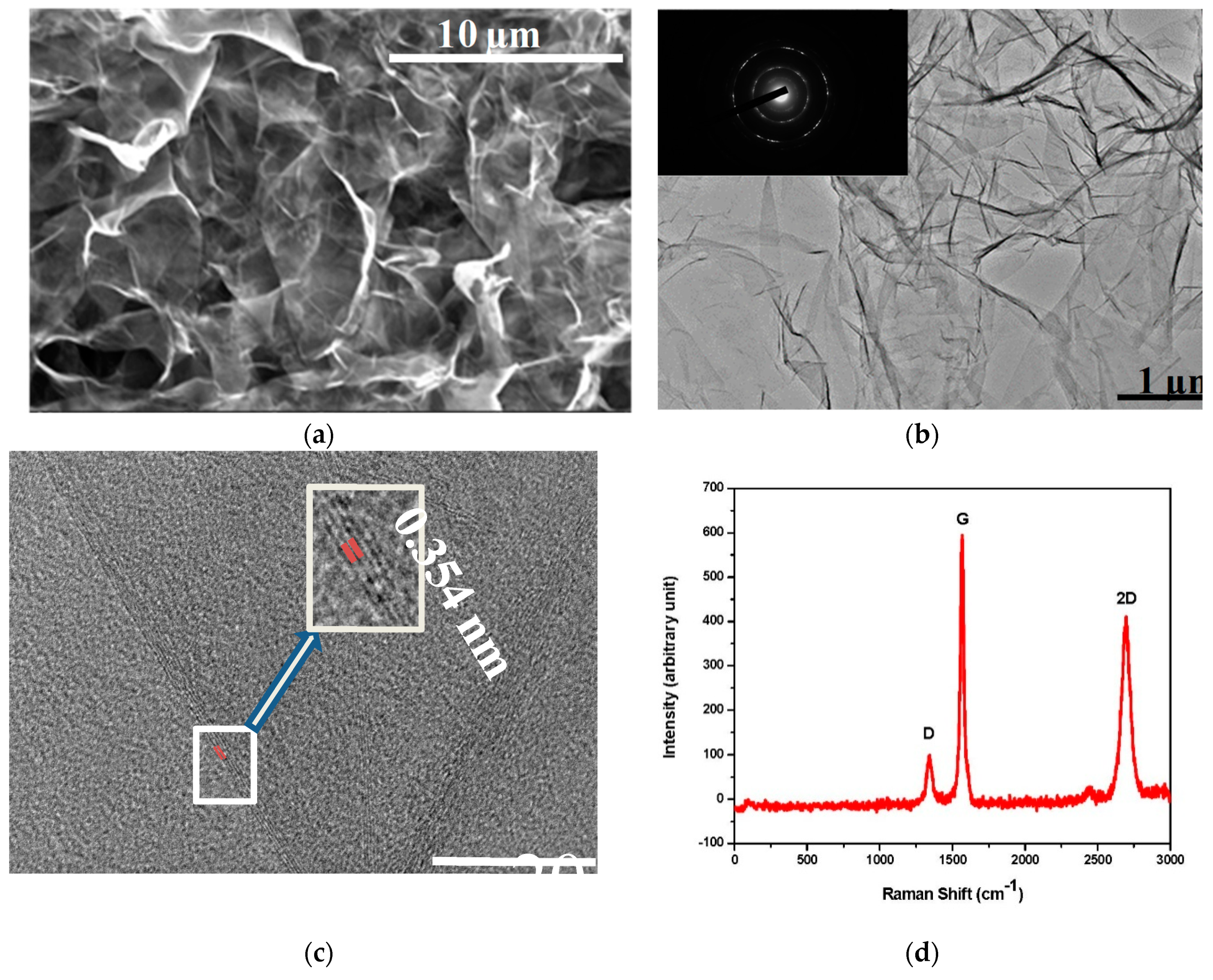
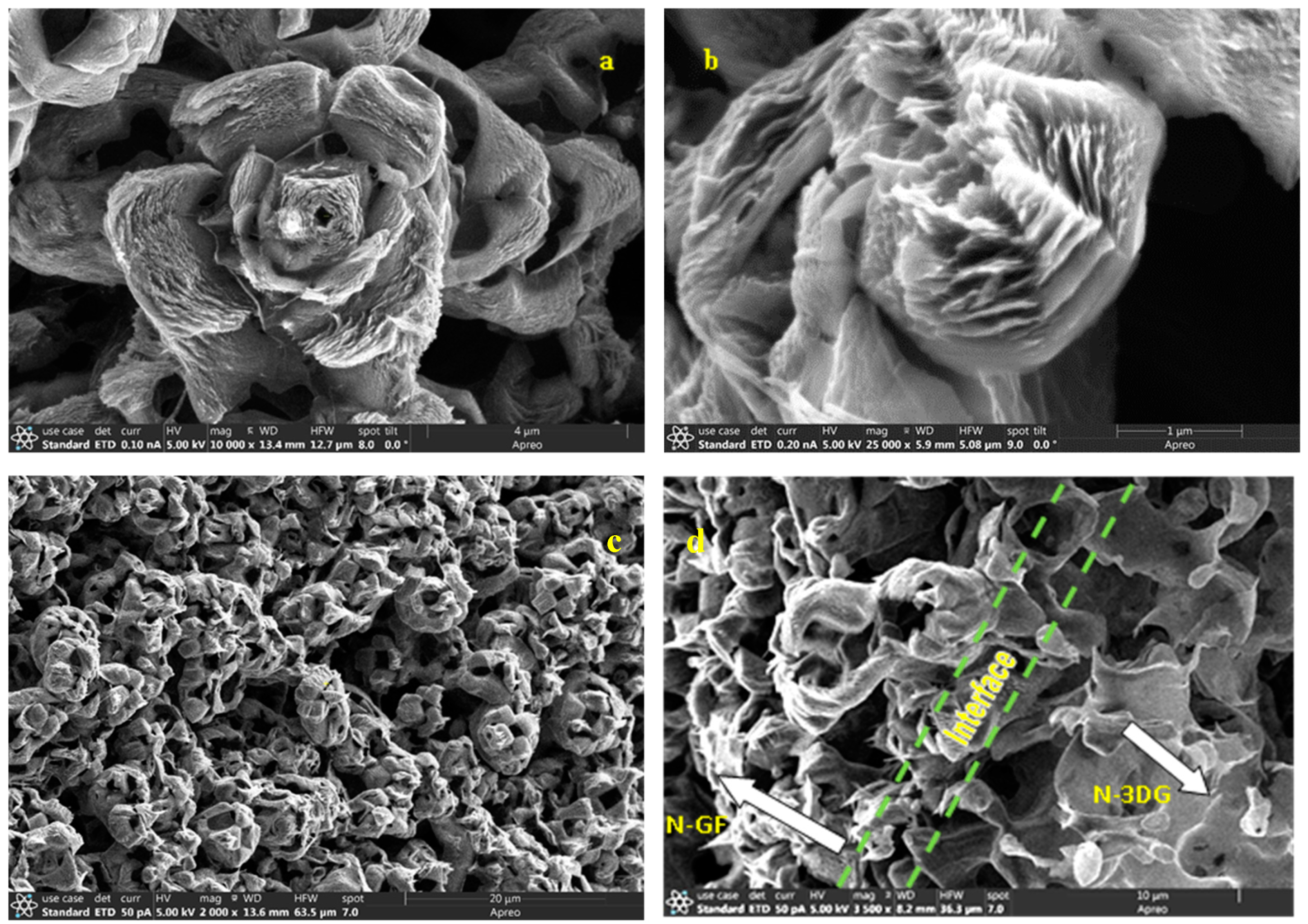
2.1. Synthesis of the 3D Graphene Hybrid Structure

Synthesis of the hybrid structure was carried out in a Black MagicTM CVD reactor manufactured by AIXTRON, Herzogenrath, Germany. At first, a catalyst framework was prepared by heat-treating (at 1000 °C in inert atmosphere) a slurry cast containing Ni powder (3–7µm, AlfraAesar), polystyrene (molecular weight ≈210,000), and diethylene glycol dibenzoate (DEGDB) in specific ratios (more details in [2]).The catalyst framework was placed in the CVD reactor and nitrogen-doped three-dimensional graphene (N-3DG) was grown in a low-pressure CVD mode (25 mbar) using 15 sccm of methane (CH4), 300 sccm of ammonia (NH3), and 1175 sccm of argon(Ar) at 850 °C. All the gases were of ultra-high purity grade. The furnace was cooled at a rate of 25 °C/min till 175 °C in order to obtain the product (H1 as per Table 1).
The resultant product was further subjected to DC plasma-enhanced CVD (PECVD) to grow vertically aligned N-doped graphene with a flower-like structure (here called N-GF) on top of N-3DG. The synthesis was carried out at 750 °C using acetylene (C2H2), NH3, and Ar at total pressure of 4 mbar and plasma power of 120W, where the Ni framework acted again as a catalyst. The concentration of C2H2 was varied in order to understand its effect on the N-GF structure (samples H2 and H3 as per Table 1). In one case, N-GF was grown over compressed N-3DG (H4). The furnace was cooled at the rate of 25 °C/min till 175 °C. The composition of the plasma was monitored using optical emission spectroscopy (Ocean Optics HR 4000 CG-UV-NIR).
After the growth, the Ni catalyst framework was dissolved in a 50% hydrochloric acid solution. The hybrid structure was washed with deionized water, ethanol, and dried. Table 1 lists the details of the experiments.

2.2. Characterization of the 3D Graphene Hybrid Structure

The structures thus obtained were characterized by various techniques. A Scanning Electron Microscope (ThermoFisherApreo, Waltham, MA, USA) was used to understand the morphology of the structure. Transmission electron microscopy (TEM) was performed to obtain finer details of the structures using a JEM 2100 (JEOL Ltd, Japan) microscope. Raman spectroscopy (Renishaw, UK, 514 nm LASER with output power of 8 miliwatt) was used to assess the defects in the structure. An average of five scans was taken for analysis. The amount of N doping was analyzed by X-ray Photoelectron Spectroscopy (XPS) using a VG Thermo-Scientific ML 3000 UHV system. A dual-anode (Mg/Al) X-ray source and a non-monochromatized Al K-alpha (1486.6 eV) radiation was used (100 W, achromatic) for the present study. For survey scan, the pass energy was CAE 100 eV with step 0.4 eV and for high resolution scan it was CAE 20 eV with step 0.025 eV. Origin 2016 software was used for fitting. The deconvolutionsof peaks were carried out using Shirley-type baseline correction and Lorentzian fitting.The water contact angle was measured by 590 Rame-hart Goniometer. Electrical conductivity was measured by Delcom 873 Interface Module non-contact sheet resistance meter. The specific surface area was estimated by the BET method (Micromeritics, Norcross, GA, USA).

2.3. Electrochemical Studies

The 3D graphene hybrid structures were laser cut into specific geometry and half cells were prepared. The electrochemical studies were conducted in 1M Na2SO4 electrolyte using GAMRY potentiostat (Warminster, PA, USA). The cyclic voltammetry (CV) was carried out using a voltage window of 0–1 V at various scan rates. The data for the Nyquist plot were acquired by varying the frequency from 105 to 0.1 Hz.

3. Results and Discussion

The obtained 3D-hybrid consists of two different structures. Initially nitrogen-doped three dimensional graphene (N-3DG) was grown over a Ni catalyst framework using LPCVD. Next, a nitrogen-doped graphene flower-like structure (N-GF) was synthesized over the N-3DG using PECVD (details in the experimental section). Figure 1a,b shows the SEM and TEM images, respectively, of N-3DG (sample H1; refer to Table 1). The SEM image reveals that interconnected graphene sheets are spread in three dimensions. The TEM image is shown in Figure 1b, where the diffraction pattern in the inset depicts the nanocrystalline feature of the 3D graphene layers. The high-resolution TEM image (Figure 1c) shows that there are 2–5 layers having interlayer spacing around 0.354 nm. Due to N doping, there are breaks in the ordered structure.
Figure 1d shows the Raman spectrum of the sample. High intensities of 2D peak (I2D) and G peak (IG) in the Raman spectrum provide information on good quality few-layered graphene. Generally, in an undoped 3D graphene the ratio (IG/I2D) can be used for calculating the number of graphene layers [42]. However, for N-doped graphene this relation may not hold well. The intensity of the 2D peak comes down and that of the D peak goes up with N doping [43,44]. The G band corresponds to the doubly degenerate E2g phonons at the Brillouin zone. The 2D and D bands are all induced by the second-order, double-resonance process and related to zone-boundary phonons. The scattering process involves two zone-boundary phonons for 2D mode; whereas, it involves one phonon and one defect for the D mode. While the D band requires defects to activate it, the 2D band does not require the activation of defects.
Once sample H1 was subjected to PECVD, beautiful flower-like structures grew over it. Figure 2a,b shows the SEM images of samples H2 and H3, respectively, which were synthesized at two different hydrocarbon concentrations (refer to Table 1 in the Experimental section). Figure 2c displays the top view of sampleH2 at low magnification and Figure 2d shows the cross-sectional image of H2. In the hybrid structure, the bottom part is N-3DG and the top part is N-GF.The number of petals of the so-called graphene flower varies with the concentration of hydrocarbon. The detailed analysis of the amount of N doping is discussed in the X-ray Photoelectron Spectroscopy (XPS) section. Typical specific surface area of the sample H2 is 330 m2/g (see Supplementary Materials).
Recently, Zhang et al. have reported growth of vertically oriented graphene nanosheets using mesoplasma chemical vapor deposition without any catalyst [45]. However, they did not produce a flower-like structure like ours. In another report, Yang et al. [46] mentioned about hollow graphene flowers having a specific surface area of 101 m2/g synthesized by Cu assisted chemical vapor deposition. Their material is the vertically aligned graphene over hollow silica spheres. The material obtained in this study is a hybrid structure consisting of a graphene flower over 3D graphene. We believe that N doping has a very important role in the growth and functionality of this 3D graphene hybrid structure. Figure 3 shows the Raman spectrum of sample H2. Synthesis under NH3 plasma has caused a good amount of N doping which in turn resulted in a high intensity of ‘D’ peak compared to that of sample H1.
In order to understand the mechanism of growth of such 3D graphene flower-like hybrid structure, we analyzed the data systematically. Figure 4 displays the SEM image of N-3DG with Ni catalyst on it, after the first step of synthesis. Elemental mapping of Ni and C inside the rectangular area shown in the SEM image depicts that the growth of graphene (i.e., distribution of C) along the grain boundary of Ni particles is less. That means that fresh Ni is available along the grain boundary for nucleation of vertical graphene flower-like structure obtained in the next step.
Figure 5 shows the SEM image of a hybrid sample just after the growth of the flower-like structure started. This image clearly shows that the petals of the flower (i.e., vertical graphene) nucleated at the boundary of the grains. In our opinion, both the electric field of plasma and N species present there play important roles in the growth of the flower-like structure.
Figure 6a,b displays the TEM images of samples H2 and H3, respectively, with diffraction patterns in the insets. Figure 6c is a high-resolution TEM image of sample H2, which shows the interface wherefrom N-GF grew over N-3DG.
Here, we propose the following mechanism based on microscopic observations at different stages of growth of the hybrid structure. After the first growth stage where N-3DG is synthesized over Ni catalyst during LPCVD, there is still active Ni catalyst available at the boundary of the Ni grains (refer to Figure 4). During the second stage of growth under PECVD, the nucleation starts at the grain boundaries initially in the horizontal direction over this active Ni catalyst. The doping of N from active species in NH3 plasma creates defects in the carbon lattice and gives an upward bend (refer to Figure 6c). The electric field in the plasma now helps in further growth in vertical direction (refer to Figure 5 and Figure 6c), which is along the applied field. A scanning TEM (STEM) image of sample H2 (Figure 7) further supports the proposed mechanism. The growth of graphene petals (N-GF) on the 3D graphene (N-3DG) after the initial bend could be observed. A schematic of the stage-wise growth of the graphene flower-like hybrid structure is given in Supplementary Materials (Figure S1).
Zhu et al. [41] also observed the formation of a thin horizontal carbon film on the substrate before the onset of vertical growth of carbon nanosheets. Further growth in the vertical direction is continued by carbon atoms supplied by C2H2. The N doping produces the wavy structure of the petals. The plasma causes a relatively larger chemical potential gradient near the surface through ion focusing effects and fast delivery of precursor. The diffusion barrier is also reduced by the electric field-induced polarization effects. The same has been proved by Zhao et al. [47] by using a continuum model. With increase in C2H2concentration, the number of petals in the flower structure increases. During the growth under the plasma environment, the gas composition also determines the nature of the structure (i.e., flower or not). When experimenting under hydrogen (H2) plasma (no ammonia, no argon), we did not obtain a flower-like structure rather a graphitic structure stacked layer-wise was yielded (Figure 8). Ghosh et al. [48] also could not obtain vertical graphene under pure hydrogen plasma. Therefore, the morphology of the vertical structure depends on the radicals present in the plasma. When NH3 plasma is used along with C2H2 as the carbon source, the plasma contains N2+, NH, C2, CN, and H as major species (see Supplementary Materials). The availability of C2 radicals is enhanced in the presence of N2. The etching of amorphous carbon is taken care of by H species. However, when pure hydrogen plasma is used, it is C2H radicals thatare dominant [47]. The etching effect is so high that the growth in the vertical direction does not happen.

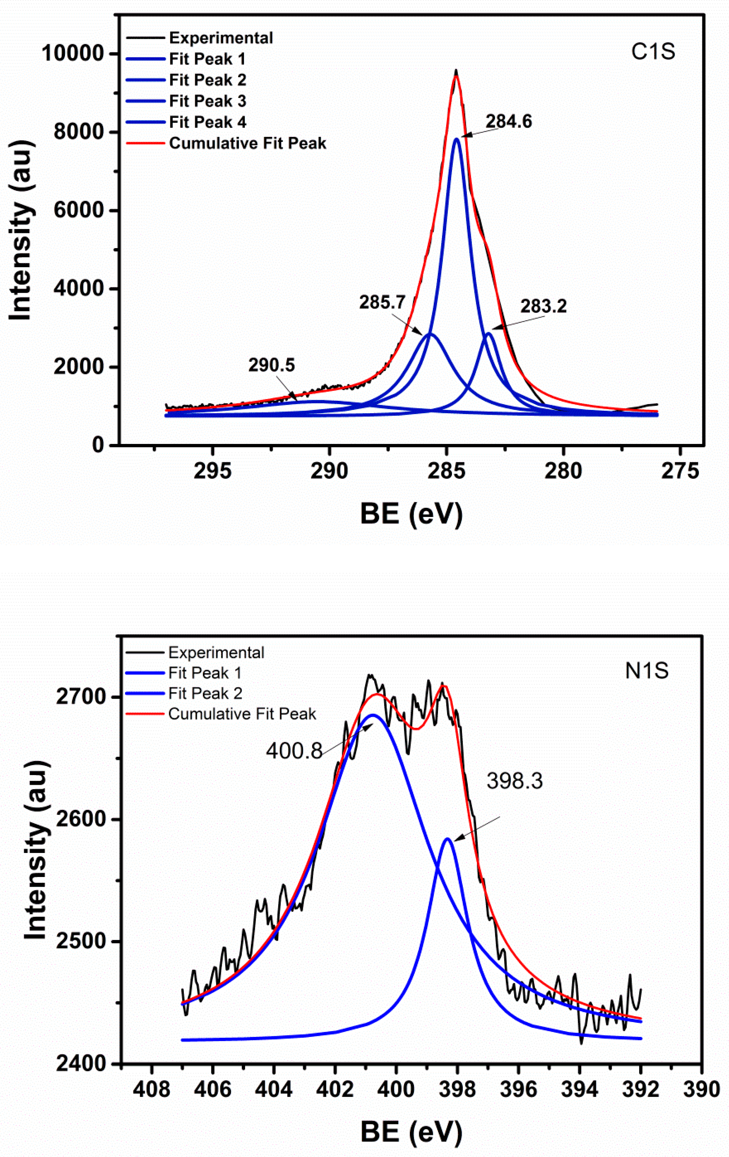
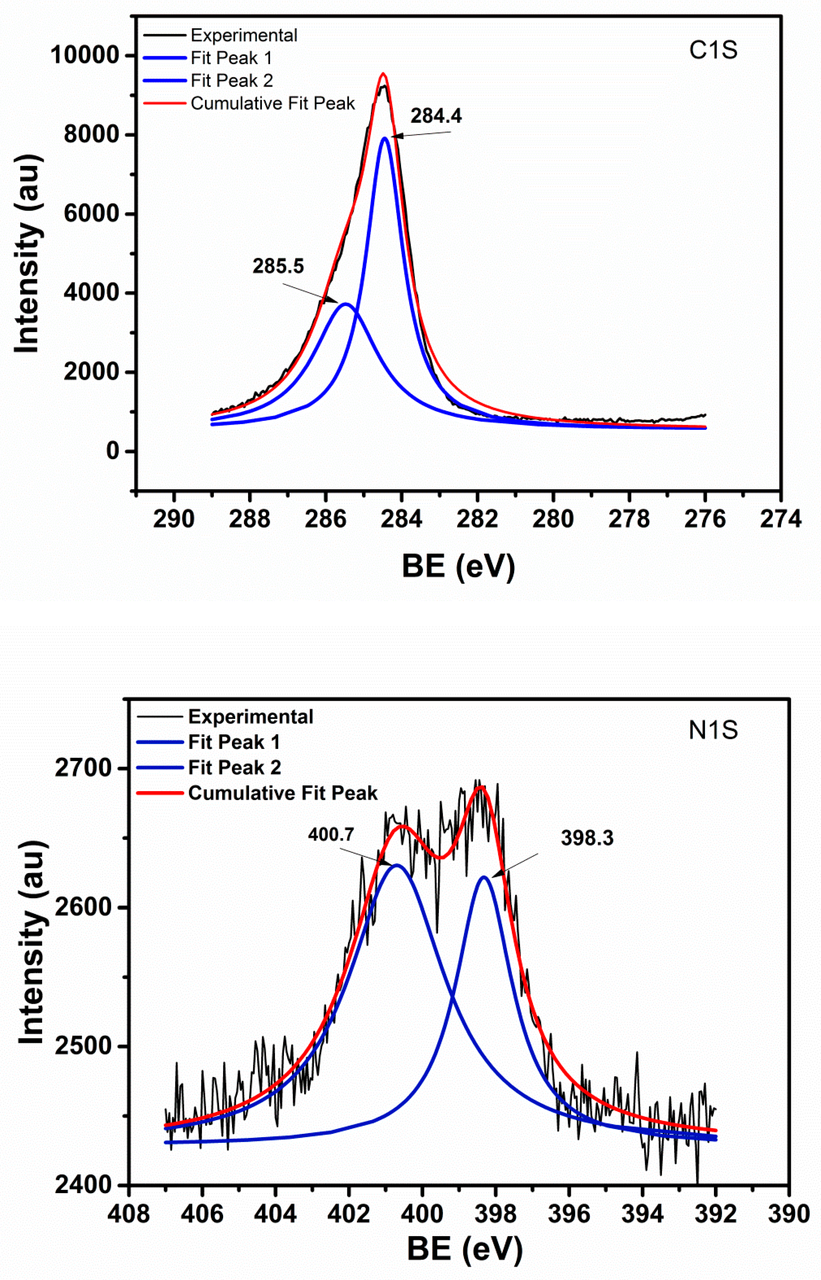
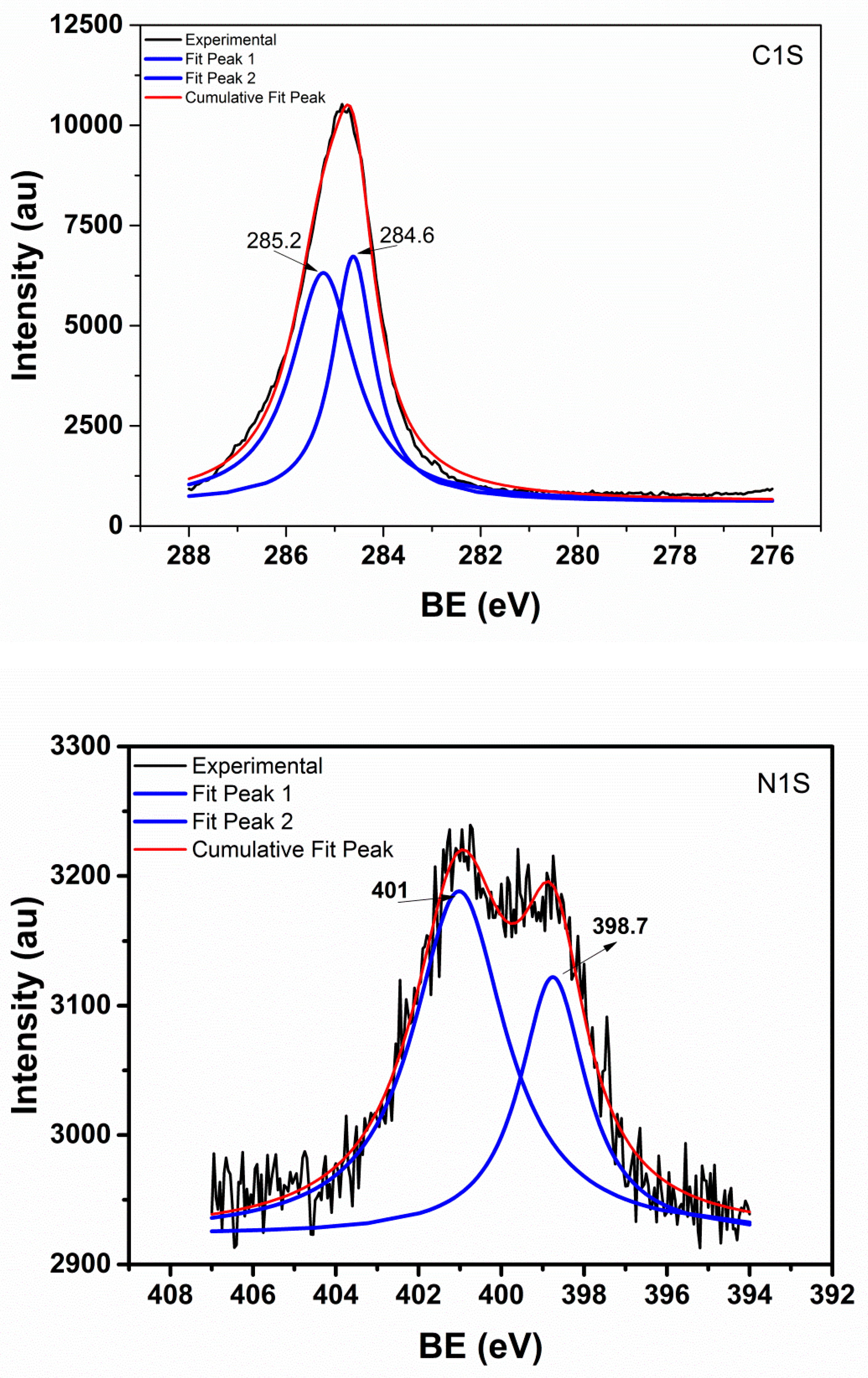
3.1. XPS Analysis of the 3D Graphene Hybrid Structures

XPS analysis was carried out to understand the nature of the bond and the amount of nitrogen doping incorporated into the samples. The survey scans are given in Supplementary Materials (Figures S6–S8). Figure 9 shows the high-resolution XPS scans of sample H1 for C1s and N1s, respectively. It is evident that N doping (3.2 at%) has taken place with NH3 even in LPCVD (without plasma).
The deconvoluted C1s shows four peaks. The peak at 283.2 eV is presumably from the residual metal carbide phase [49]. The peak at 284.6 eV corresponds to the C−C bond in graphene and that at 285.7 eV is assigned to the C=N bond [50,51]. The peak at 290.5 eV corresponds to O=C−O bond [52]. A small amount of O is always present in the surface. If N1s is deconvoluted, two peaks appear at 398.3 and 400.8 eV, corresponding to pyridinic N and graphitic N [50].
XPS analysis also shows that samples H2 and H3 contain 6.1 and 7.2 at% of N, respectively. As these samples were synthesized under NH3 plasma, more N doping with respect to the sample H1 has taken place. As the concentration of NH3 was greater for sample H3 compared to sample H2, it resulted in maximum N doping.
Figure 10 shows the deconvoluted peaks of C1s and N1s for sample H2. Peak at 284.4 eV is assigned to the C−C bond and that at 285.5 eV corresponds to C=N bonding. Peaks at 398.3 and 400.7 eV correspond to pyridinic N and graphitic N, respectively.
Figure 11 shows the deconvoluted peaks of C1s and N1s for sample H3. C1s has two peaks at 284.6 and 285.2 eV corresponding to the C−C bond and C=N, respectively. Interestingly, N1s revealed pyridinic N (398.7 eV) and graphitic N (401.0 eV).
It is worth mentioning that high resolution scans over a wider binding energy range (both for C1s and N1s for all the samples) are expected to provide more accurate surface chemistry information.

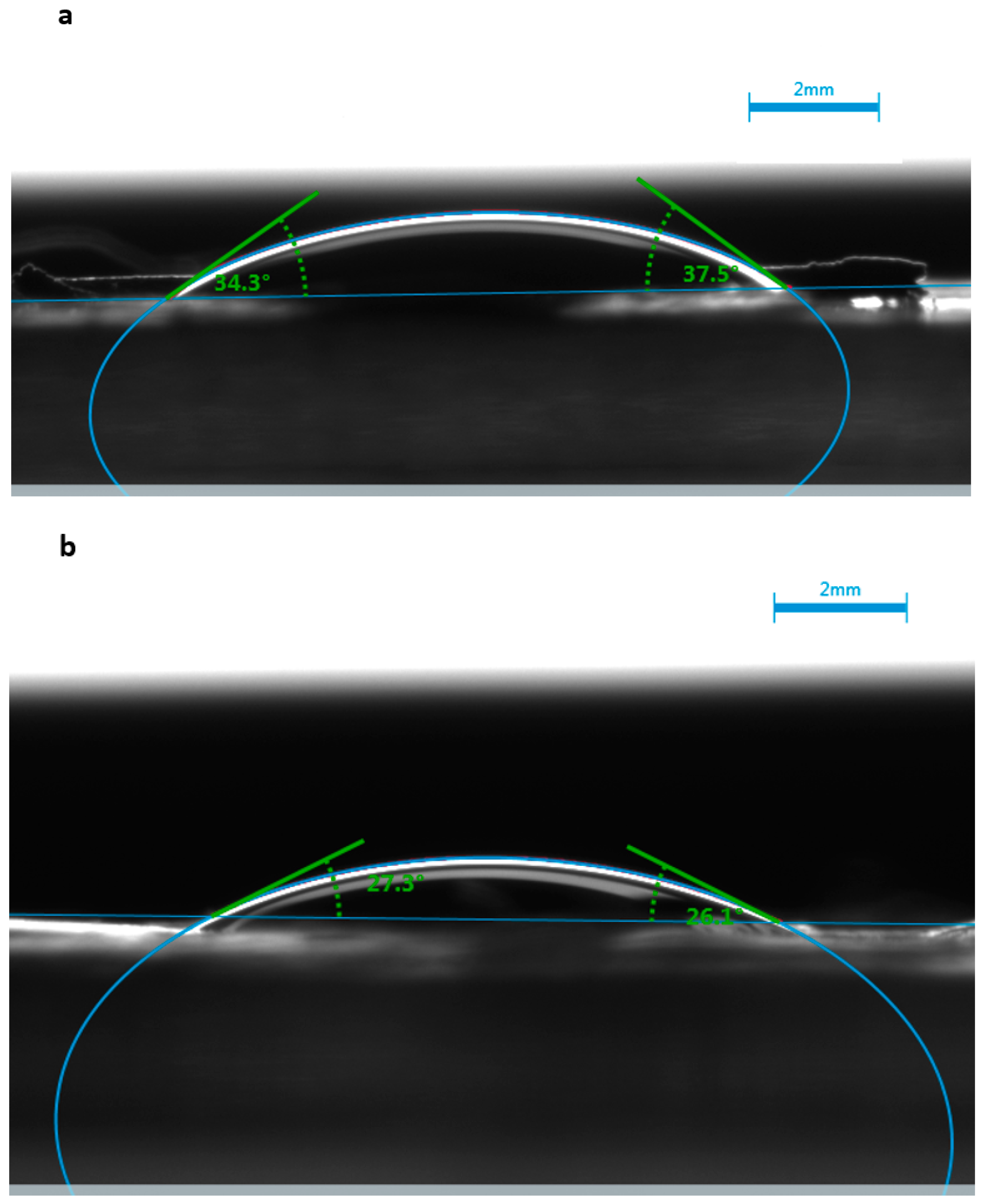
3.2. Contact Angle Measurements

Pristine graphene, in general, is hydrophobic. The N doping is supposed to make the structure more hydrophilic due to surface functionalization. In order to test the hydrophilicity, water contact angle was measured for samples H1, H2, and H3.
Figure 12a,b shows the images of water angles for samples H1 and H2. The contact angle for sample H1 was around 35° and that of sample H2 was around 25°. The contact angle for sample H3 was zero. With an increase in N content, the hydrophilicity has increased.

3.3. Electrical Conductivity

Sample H1, which is N doped 3DG, showed an electrical conductivity value of 22 S/cm which is slightly higher than undoped 3DG (≈16 S/cm). The hybrid structures H2 and H3 revealed increase in the electrical conductivity values to 35 and 38 S/cm, respectively. Since samples H1, H2, and H3 are porous structures, the electrical conductivities are not very high. The conductivity could be improved by roll pressing N-3DG and then growing N-GF on top of the flattened graphene surface. Sample H4 was synthesized in that way and the electrical conductivity increased to 374 S/cm. However, roll passing results in collapsing of pores in 3DG, which is detrimental for electrochemical energy storage but good for sensing application.

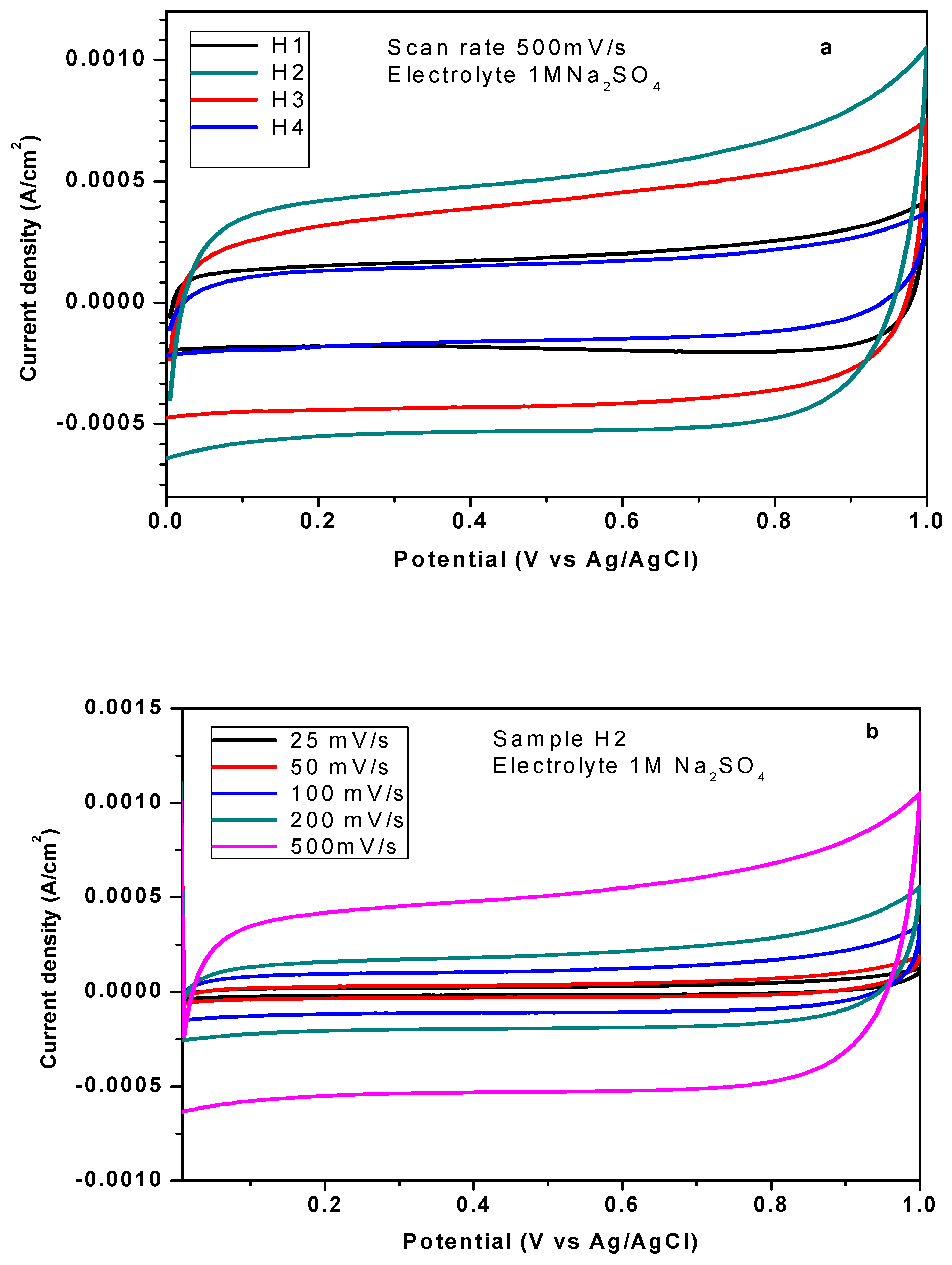
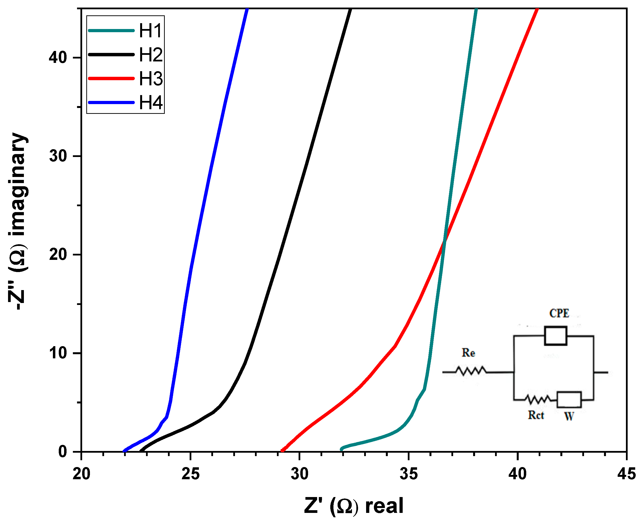
3.4. Electrochemical Properties

Figure 13a,b shows the electrochemical response of the samples synthesized at different conditions (samples H1–H4) using CV in 1M Na2SO4 electrolyte against an Ag/AgCl reference electrode. It can be observed from Figure 13a that all the samples behave like electrical double-layer capacitors (EDLC) even at a scan rate as high as 500 mV/s. The hybrid structures H2 and H3 (N-3DG+N-GF) are showing much higher area normalized specific capacitance with respect to sample H1 (containing only N-3DG). However, the electrochemical performance went down for sample H4, which was compressed and thus was having less porosity for effective ion mobility and penetration. N-doping has increased the performance of these structures several fold. The best performance was shown by sample H2. Figure 13b shows the CV plots for sample H2 at different scan rates.
The Nyquist plot for samples H1–H4 is shown in Figure 14. The measured impedance spectra can be fitted with an equivalent circuit (inset in Figure 14) consisting of a bulk electrolyte resistance Re, a charge transfer resistance Rct, a pseudocapacitive element W, and a constant phase element CPE. The values of Rct can be obtained from the semicircle at high frequency. Samples H1, H2, and H3 have low Rct values between 2 and 3 Ω. This indicates high charge transfer efficiency at the interface between electrode and electrolyte. N doping in these structures has resulted in lowering of Rct. For sample H4 the value of Rct went down further to 1 Ω. This is due to compression of the 3DG layers, which improved the electrical conductivity. The hybrid structures (H2–H4) also showed better Re with respect to N-3DG (sample H1) alone.
The advantage of the hybrid structure created in this work based on 3D graphene is that it reveals low Rct, high surface area, and good EDLC behavior. If pseudo-supercapacitive active material is loaded into this structure, it is expected to show very high specific capacitance. In one such case, we loaded polyaniline (PANI) and could achieve a specific capacitance of 190 F/g with area capacitance of 413 mF/cm2. A typical CV curve with PANI loaded H2 is given in the Supplementary Materials (Figure S9). Detailed results on the electrochemical performance of PANI loaded hybrid structures will be communicated shortly. Similarly, the N doped hybrid material reported here can be a better choice over 3D graphene alone for sensor and battery applications.

4. Conclusions

Nitrogen-doped nano-carbon hybrid structures consisting of vertical graphene with a flower-like morphology and 3D graphene could be synthesized using a combination of LPCVD and PECVD. The NH3 plasma along with the electrical field that generates it has an active role in the growth of this unique structure. Up to 7.2 at% N could be doped into the obtained hybrid materials thanks to the plasma environment. The acquired Raman spectra showed a decrease in the 2D band and an increase in D band intensities due to N doping. A possible growth mechanism was proposed based on the microscopic and spectroscopic observations. N doping also increased the wettability of the material. The grown hybrid structures showed promising electrochemical behavior making them suitable for advanced energy storage and sensing applications.

Supplementary Materials

The following are available online at https://0-www-mdpi-com.brum.beds.ac.uk/2311-5629/6/2/40/s1, Figure S1: Schematic of the stage-wise growth of graphene flower-like hybrid structure, Figure S2: Nitrogen Adsorption-Desorption Isotherm for sample H2, Figure S3:BET Plot of sample H2, Figure S4: Pore size distribution (H–K) of sample H2, Figure S5: Optical emission spectra of NH3-C2H2 plasma during synthesis of sample H2, Figure S6: Wide scan spectra of sample H1 showing C, N and O peaks, Figure S7: Wide scan spectra of sample H2 showing C, N and O peaks, Figure S8: Wide scan spectra of sample H3 showing C, N and O peaks, Figure S9: Huge improvement in electrochemical property with PANI incorporation in sample H2.

Author Contributions

Conceptualization, K.D.; methodology, K.D.; formal analysis, K.D., M.K. and S.S.; investigation, K.D., M.K. and J.K.; resources, K.D., M.K. P.K.A. and S.N.K.; data curation, M.K.; writing—original draft preparation, K.D.; writing—review and editing, V.S.; supervision, V.S.; project administration, V.S.; funding acquisition, K.D. and V.S. All authors have read and agreed to the published version of the manuscript.

Funding

This research received no external funding.

Acknowledgments

K.D. would like to thank Fulbright Foundation and USIEF for providing fellowship. K.D. also acknowledges the help of Siddharth Mishra and Nalin Rupesinghe for Black Magic operation. K.D. also thanks Rajath Alexander for help in preparing some figures.

Conflicts of Interest

The authors declare no conflict of interest.

References

  1. Chen, Z.; Ren, W.; Gao, L.; Liu, B.; Pei, S.; Cheng, H.-M. Three-dimensional flexible and conductive interconnected graphene networks grown by chemical vapour deposition. Nat. Mater. 2011, 10, 424–428. [Google Scholar] [CrossRef] [PubMed]
  2. Zhang, L.; DeArmond, D.; Alvarez, N.T.; Zhao, D.; Wang, T.; Hou, G.; Malik, R.; Heineman, W.R.; Shanov, V. Beyond graphene foam, a new form of three-dimensional graphene for supercapacitor electrodes. J. Mater. Chem. A 2016, 4, 1876–1886. [Google Scholar] [CrossRef]
  3. Zhang, Q.; Chen, W.; Yu, Y.; Lin, D.; Fisher, T.S.; Xu, X.; Li, H.; Xiong, G. Hyperbolically Patterned 3D Graphene Metamaterial with Negative Poisson’s Ratio and Superelasticity. Adv. Mater. 2016, 28, 2229–2237. [Google Scholar] [CrossRef]
  4. Alvarez, N.; DeArmond, D.; Malik, R.; Shanov, V.N.; Zhang, L. Graphene Paper and a Process for Making Graphene Paper and a Graphene Electrode. U.S. Patent Application No. 15/619, 388, 9 June 2017. [Google Scholar]
  5. Yu, X.; Lu, B.; Xu, Z. Super long-life supercapacitors based on the construction of nanohoneycomb-like strongly coupled CoMoO4–3D graphene hybrid electrodes. Adv. Mater. 2014, 26, 1044–1051. [Google Scholar] [CrossRef] [PubMed]
  6. Dong, X.-C.; Xu, H.; Wang, X.-W.; Huang, Y.-X.; Chan-Park, M.B.; Zhang, H.; Wang, L.-H.; Huang, W.; Chen, P. 3D graphene–cobalt oxide electrode for high-performance supercapacitor and enzymeless glucose detection. ACS Nano 2012, 6, 3206–3213. [Google Scholar] [CrossRef]
  7. He, Y.; Chen, W.; Li, X.; Zhang, Z.; Fu, J.; Zhao, C.; Xie, E. Freestanding three-dimensional graphene/MnO2 composite networks as ultralight and flexible supercapacitor electrodes. ACS Nano 2013, 7, 174–182. [Google Scholar] [CrossRef]
  8. Dong, X.; Wang, X.; Wang, J.; Song, H.; Li, X.; Wang, L.; Chan-Park, M.B.; Li, C.M.; Chen, P. Synthesis of a MnO2–graphene foam hybrid with controlled MnO2 particle shape and its use as a supercapacitor electrode. Carbon N. Y. 2012, 50, 4865–4870. [Google Scholar] [CrossRef]
  9. Zhao, C.; Zheng, W.; Wang, X.; Zhang, H.; Cui, X.; Wang, H. Ultrahigh capacitive performance from both Co (OH)2/graphene electrode and K3 Fe (CN)6 electrolyte. Sci. Rep. 2013, 3, 2986. [Google Scholar] [CrossRef]
  10. Cao, X.; Shi, Y.; Shi, W.; Lu, G.; Huang, X.; Yan, Q.; Zhang, Q.; Zhang, H. Preparation of novel 3D graphene networks for supercapacitor applications. Small 2011, 7, 3163–3168. [Google Scholar] [CrossRef] [PubMed]
  11. Luo, J.; Liu, J.; Zeng, Z.; Ng, C.F.; Ma, L.; Zhang, H.; Lin, J.; Shen, Z.; Fan, H.J. Three-dimensional graphene foam supported Fe3O4 lithium battery anodes with long cycle life and high rate capability. Nano Lett. 2013, 13, 6136–6143. [Google Scholar] [CrossRef] [PubMed]
  12. Li, N.; Chen, Z.; Ren, W.; Li, F.; Cheng, H.-M. Flexible graphene-based lithium ion batteries with ultrafast charge and discharge rates. Proc. Natl. Acad. Sci. USA 2012, 109, 17360–17365. [Google Scholar] [CrossRef] [PubMed] [Green Version]
  13. Zhou, G.; Li, L.; Ma, C.; Wang, S.; Shi, Y.; Koratkar, N.; Ren, W.; Li, F.; Cheng, H.-M. A graphene foam electrode with high sulfur loading for flexible and high energy Li-S batteries. Nano Energy 2015, 11, 356–365. [Google Scholar] [CrossRef]
  14. Zhang, W.; Zhu, J.; Ang, H.; Zeng, Y.; Xiao, N.; Gao, Y.; Liu, W.; Hng, H.H.; Yan, Q. Binder-free graphene foams for O2 electrodes of Li–O2 batteries. Nanoscale 2013, 5, 9651–9658. [Google Scholar] [CrossRef] [PubMed]
  15. Pan, F.; Chen, S.; Li, Y.; Tao, Z.; Ye, J.; Ni, K.; Yu, H.; Xiang, B.; Ren, Y.; Qin, F. 3D graphene films enable simultaneously high sensitivity and large stretchability for strain sensors. Adv. Funct. Mater. 2018, 28, 1803221. [Google Scholar] [CrossRef]
  16. Nag, A.; Mitra, A.; Mukhopadhyay, S.C. Graphene and its sensor-based applications: A review. Sens. Actuators A Phys. 2018, 270, 177–194. [Google Scholar] [CrossRef]
  17. Deng, T.; Zhang, Z.; Liu, Y.; Wang, Y.; Su, F.; Li, S.; Zhang, Y.; Li, H.; Chen, H.; Zhao, Z. Three-dimensional graphene field-effect transistors as high-performance photodetectors. Nano Lett. 2019, 19, 1494–1503. [Google Scholar] [CrossRef] [Green Version]
  18. Idowu, A.; Boesl, B.; Agarwal, A. 3D graphene foam-reinforced polymer composites—A review. Carbon N. Y. 2018, 135, 52–71. [Google Scholar] [CrossRef]
  19. Qiu, H.; Du, P.; Hu, K.; Gao, J.; Li, H.; Liu, P.; Ina, T.; Ohara, K.; Ito, Y.; Chen, M. Metal and Nonmetal Codoped 3D Nanoporous Graphene for Efficient Bifunctional Electrocatalysis and Rechargeable Zn–Air Batteries. Adv. Mater. 2019, 31, 1900843. [Google Scholar] [CrossRef]
  20. Kakavelakis, G.; Maksudov, T.; Konios, D.; Paradisanos, I.; Kioseoglou, G.; Stratakis, E.; Kymakis, E. Efficient and highly air stable planar inverted perovskite solar cells with reduced graphene oxide doped PCBM electron transporting layer. Adv. Energy Mater. 2017, 7, 1602120. [Google Scholar] [CrossRef]
  21. Shao, X.; Khursheed, A. A Review Paper on “Graphene Field Emission for Electron Microscopy. ” Appl. Sci. 2018, 8, 868. [Google Scholar] [CrossRef] [Green Version]
  22. Hiramatsu, M.; Hori, M. Carbon Nanowalls: Synthesis and Emerging Applications; Springer Science & Business Media: Wien, London, 2010; ISBN 3211997180. [Google Scholar]
  23. Chen, J.; Bo, Z.; Lu, G. Vertically-Oriented Graphene; Springer International Publishing: Cham, Switzerland, 2015; Volume 10, ISBN 978-3-319-15301-8. [Google Scholar]
  24. Shang, N.G.; Papakonstantinou, P.; McMullan, M.; Chu, M.; Stamboulis, A.; Potenza, A.; Dhesi, S.S.; Marchetto, H. Catalyst-free efficient growth, orientation and biosensing properties of multilayer graphene nanoflake films with sharp edge planes. Adv. Funct. Mater. 2008, 18, 3506–3514. [Google Scholar] [CrossRef]
  25. Zhang, Z.; Lee, C.; Zhang, W. Vertically aligned graphene nanosheet arrays: Synthesis, properties and applications in electrochemical energy conversion and storage. Adv. Energy Mater. 2017, 7, 1700678. [Google Scholar] [CrossRef] [Green Version]
  26. Seo, D.H.; Kumar, S.; Ostrikov, K. Control of morphology and electrical properties of self-organized graphenes in a plasma. Carbon N. Y. 2011, 49, 4331–4339. [Google Scholar] [CrossRef]
  27. Thomas, R.; Rao, G.M. Synthesis of 3-dimensional porous graphene nanosheets using electron cyclotron resonance plasma enhanced chemical vapour deposition. RSC Adv. 2015, 5, 84927–84935. [Google Scholar] [CrossRef]
  28. Ghosh, S.; Ganesan, K.; Polaki, S.R.; Mathews, T.; Dhara, S.; Kamruddin, M.; Tyagi, A.K. Influence of substrate on nucleation and growth of vertical graphene nanosheets. Appl. Surf. Sci. 2015, 349, 576–581. [Google Scholar] [CrossRef]
  29. Davami, K.; Shaygan, M.; Kheirabi, N.; Zhao, J.; Kovalenko, D.A.; Rümmeli, M.H.; Opitz, J.; Cuniberti, G.; Lee, J.-S.; Meyyappan, M. Synthesis and characterization of carbon nanowalls on different substrates by radio frequency plasma enhanced chemical vapor deposition. Carbon N. Y. 2014, 72, 372–380. [Google Scholar] [CrossRef]
  30. Choi, J.W.; Youn, S.K.; Park, H.G. Carbon micronymphaea: Graphene on vertically aligned carbon nanotubes. J. Nanomater. 2013, 2013, 7. [Google Scholar] [CrossRef]
  31. Zhang, M.; Alvarez, N.T.; Zhao, D.; Zhang, L.; Haase, M.R.; Malik, R.; Katuscak, C.; Wang, T.; Shanov, V. A corrugated graphene–carbon nanotube composite as electrode material. Nano Life 2014, 4, 1441019. [Google Scholar] [CrossRef]
  32. Zhao, J.; Xing, B.; Yang, H.; Pan, Q.; Li, Z.; Liu, Z. Growth of carbon nanotubes on graphene by chemical vapor deposition. New Carbon Mater. 2016, 31, 31–36. [Google Scholar] [CrossRef]
  33. Kim, Y.-S.; Kumar, K.; Fisher, F.T.; Yang, E.-H. Out-of-plane growth of CNTs on graphene for supercapacitor applications. Nanotechnology 2011, 23, 15301. [Google Scholar] [CrossRef]
  34. Wu, S.; Shi, E.; Yang, Y.; Xu, W.; Li, X.; Cao, A. Direct fabrication of carbon nanotube-graphene hybrid films by a blown bubble method. Nano Res. 2015, 8, 1746–1754. [Google Scholar] [CrossRef]
  35. Harris, P.J.F.; Suarez-Martinez, I.; Marks, N.A. The structure of junctions between carbon nanotubes and graphene shells. Nanoscale 2016, 8, 18849–18854. [Google Scholar] [CrossRef] [PubMed]
  36. He, J.; Chen, Y.; Lv, W.; Wen, K.; Li, P.; Wang, Z.; Zhang, W.; Qin, W.; He, W. Three-dimensional hierarchical graphene-CNT@ Se: A highly efficient freestanding cathode for Li–Se batteries. ACS Energy Lett. 2016, 1, 16–20. [Google Scholar] [CrossRef]
  37. Inagaki, M.; Toyoda, M.; Soneda, Y.; Morishita, T. Nitrogen-doped carbon materials. Carbon N. Y. 2018, 132, 104–140. [Google Scholar] [CrossRef]
  38. Faisal, S.N.; Haque, E.; Noorbehesht, N.; Zhang, W.; Harris, A.T.; Church, T.L.; Minett, A.I. Pyridinic and graphitic nitrogen-rich graphene for high-performance supercapacitors and metal-free bifunctional electrocatalysts for ORR and OER. RSC Adv. 2017, 7, 17950–17958. [Google Scholar] [CrossRef] [Green Version]
  39. Barsan, M.M.; Prathish, K.P.; Sun, X.; Brett, C.M.A. Nitrogen doped graphene and its derivatives as sensors and efficient direct electron transfer platform for enzyme biosensors. Sens. Actuators B Chem. 2014, 203, 579–587. [Google Scholar] [CrossRef]
  40. Lin, Y.-C.; Teng, P.-Y.; Yeh, C.-H.; Koshino, M.; Chiu, P.-W.; Suenaga, K. Structural and chemical dynamics of pyridinic-nitrogen defects in graphene. Nano Lett. 2015, 15, 7408–7413. [Google Scholar] [CrossRef] [PubMed]
  41. Zhu, M.; Wang, J.; Holloway, B.C.; Outlaw, R.A.; Zhao, X.; Hou, K.; Shutthanandan, V.; Manos, D.M. A mechanism for carbon nanosheet formation. Carbon N. Y. 2007, 45, 2229–2234. [Google Scholar] [CrossRef]
  42. Das, A.; Chakraborty, B.; Sood, A.K. Raman spectroscopy of graphene on different substrates and influence of defects. Bull. Mater. Sci. 2008, 31, 579–584. [Google Scholar] [CrossRef]
  43. Yanilmaz, A.; Tomak, A.; Akbali, B.; Bacaksiz, C.; Ozceri, E.; Ari, O.; Senger, R.T.; Selamet, Y.; Zareie, H.M. Nitrogen doping for facile and effective modification of graphene surfaces. RSC Adv. 2017, 7, 28383–28392. [Google Scholar] [CrossRef] [Green Version]
  44. Maddi, C.; Bourquard, F.; Barnier, V.; Avila, J.; Asensio, M.-C.; Tite, T.; Donnet, C.; Garrelie, F. Nano-Architecture of nitrogen-doped graphene films synthesized from a solid CN source. Sci. Rep. 2018, 8, 3247. [Google Scholar] [CrossRef] [PubMed]
  45. Zhang, H.; Wu, S.; Lu, Z.; Chen, X.; Chen, Q.; Gao, P.; Yu, T.; Peng, Z.; Ye, J. Efficient and controllable growth of vertically oriented graphene nanosheets by mesoplasma chemical vapor deposition. Carbon N. Y. 2019, 147, 341–347. [Google Scholar] [CrossRef]
  46. Yang, J.; Qian, X.; Li, H.; Wang, H.; Xue, X.; Cai, L.; Hu, P.; Yu, G. Novel Hollow Graphene Flowers Synthesized by Cu-Assisted Chemical Vapor Deposition. Adv. Mater. Interfaces 2018, 5, 1800347. [Google Scholar] [CrossRef]
  47. Zhao, J.; Shaygan, M.; Eckert, J.; Meyyappan, M.; Rümmeli, M.H. A growth mechanism for free-standing vertical graphene. Nano Lett. 2014, 14, 3064–3071. [Google Scholar] [CrossRef] [PubMed]
  48. Ghosh, S.; Ganesan, K.; Polaki, S.R.; Ilango, S.; Amirthapandian, S.; Dhara, S.; Kamruddin, M.; Tyagi, A.K. Flipping growth orientation of nanographitic structures by plasma enhanced chemical vapor deposition. RSC Adv. 2015, 5, 91922–91931. [Google Scholar] [CrossRef] [Green Version]
  49. Bayer, B.C.; Bosworth, D.A.; Michaelis, F.B.; Blume, R.; Habler, G.; Abart, R.; Weatherup, R.S.; Kidambi, P.R.; Baumberg, J.J.; Knop-Gericke, A. In situ observations of phase transitions in metastable nickel (carbide)/carbon nanocomposites. J. Phys. Chem. C 2016, 120, 22571–22584. [Google Scholar] [CrossRef] [Green Version]
  50. Zhao, R.; Afaneh, T.; Dharmasena, R.; Jasinski, J.; Sumanasekera, G.; Henner, V. Study of nitrogen doping of graphene via in-situ transport measurements. Phys. B Condens. Matter 2016, 490, 21–24. [Google Scholar] [CrossRef]
  51. Dementjev, A.P.; De Graaf, A.; Van de Sanden, M.C.M.; Maslakov, K.I.; Naumkin, A.V.; Serov, A.A. X-Ray photoelectron spectroscopy reference data for identification of the C3N4 phase in carbon–nitrogen films. Diam. Relat. Mater. 2000, 9, 1904–1907. [Google Scholar] [CrossRef]
  52. Desimoni, E.; Brunetti, B. X-ray photoelectron spectroscopic characterization of chemically modified electrodes used as chemical sensors and biosensors: A review. Chemosensors 2015, 3, 70–117. [Google Scholar] [CrossRef] [Green Version]
Figure 1. (a) SEM image of nitrogen-doped three-dimensional graphene (N-3DG) (sample H1) showing interconnected graphene flakes. (b) TEM image of sample H1 with diffraction pattern (inset). (c) HRTEM image showing graphene layers. (d) Raman spectrum of sample H1 showing pronounced presence of D peak due to N-doping.
Carbon 06 00040 g001
Figure 2. SEM images of N doped graphene flower (a) with 20% C2H2-sample H2, (b) with 5% C2H2-sample H3, (c) low magnification top view of sample H2 showing distribution of N-GF, (d) cross sectional image of H2 illustrating N-3DG, N-GF, and the interface between them.
Carbon 06 00040 g002
Figure 3. Raman spectrum of sample H2 showing presence of increased D peak and decreased 2D peak due to more N-doping.
Carbon 06 00040 g003
Figure 4. Mapping of C and Ni along the grain boundary of sample H1.
Carbon 06 00040 g004
Figure 5. SEM image showing early stage growth of N-GF from boundary of N-3DG flakes.
Carbon 06 00040 g005
Figure 6. (a) TEM image of sample H2 (inset diffraction pattern), (b) TEM image of sample H3 (inset diffraction pattern), (c) HRTEM image of H2 showing interface of N-3DG and N-GF.
Carbon 06 00040 g006
Figure 7. Scanning TEM (STEM) image of sample H2.
Carbon 06 00040 g007
Figure 8. Graphitic structure obtained in hydrogen plasma.
Carbon 06 00040 g008
Figure 9. Deconvolution and Lorentzian fit to X-ray Photoelectron Spectroscopy (XPS) data for C1s and N1s peaks of sample H1.
Carbon 06 00040 g009
Figure 10. Deconvolution and Lorentzian fit to XPS data for C1s and N1s peaks of sample H2.
Carbon 06 00040 g010
Figure 11. Deconvolution and Lorentzian fit to XPS data for C1s and N1s peaks of sample H3.
Carbon 06 00040 g011
Figure 12. Contact angle analysis for samples (a) H1 and (b) H2 showing increase in hydrophilicity with N doping.
Carbon 06 00040 g012
Figure 13. (a) Comparative cyclic voltammetry (CV) profiles of samples H1–H4 at 500 mV/s, (b) CV profiles of sample H2 at different scan rates.
Carbon 06 00040 g013
Figure 14. Nyquist plot for samples H1–H4.
Carbon 06 00040 g014
Table 1. Experimental matrix for growth of N-doped 3D graphene hybrid structures.
Sample IDGrowth of N-3DGRoll PassGrowth of N-GFRemarks
H1YesNoNoWith 1% CH4 using LPCVD
H2YesNoYesWith 1% CH4 using LPCVD followed by 20% C2H2 using PECVD
H3YesNoYesWith 1% CH4 using LPCVD followed by 5% C2H2 using PECVD
H4YesYes YesN-3DG was compressed between rollers having a gap 0.35mm prior to growth of N-GF with 20% C2H2

