Detection of Spin Polarized Band in VO2/TiO2(001) Strained Films via Orbital Selective Constant Initial State Spectroscopy

 , , , , , and
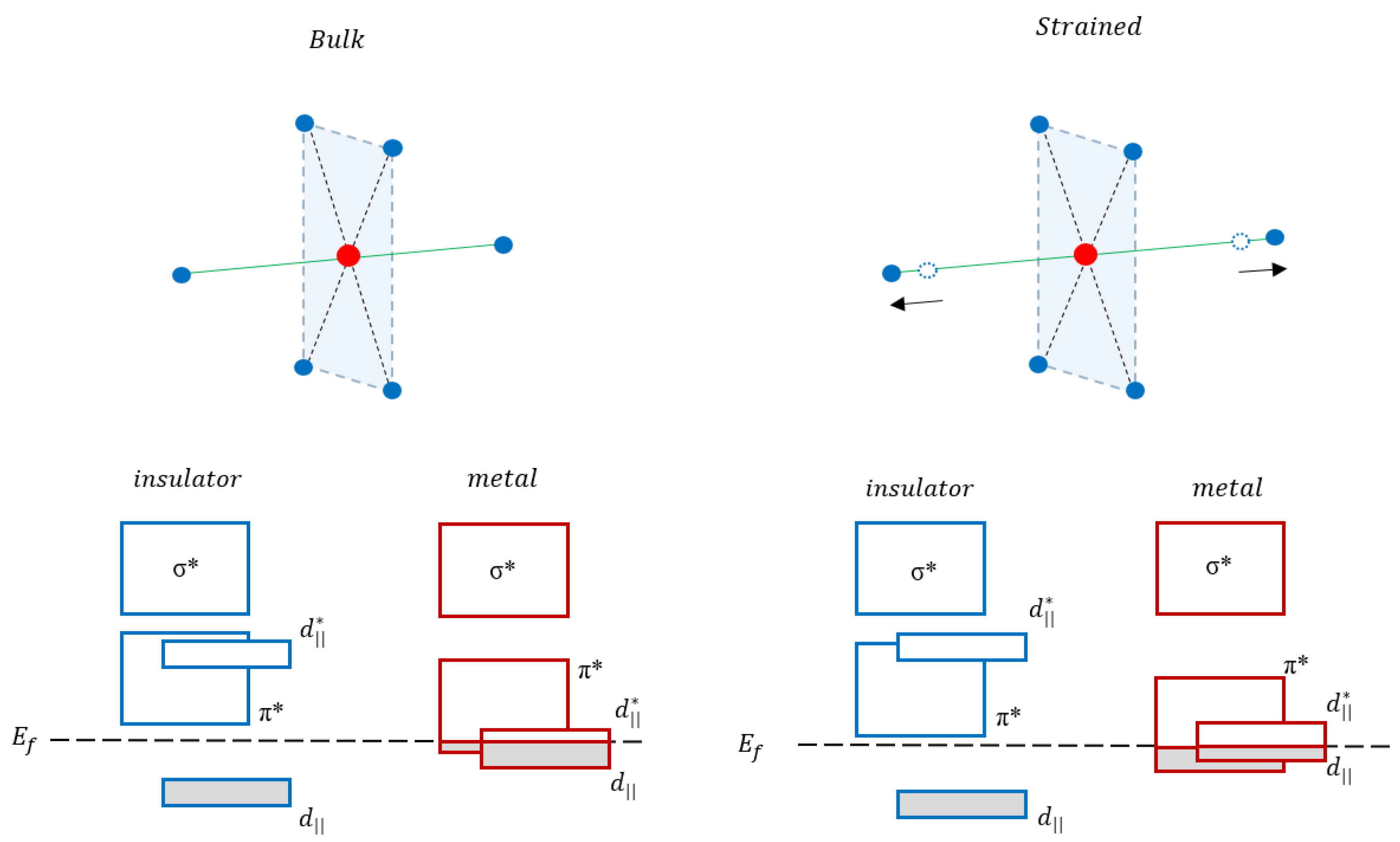
Abstract
:1. Introduction
2. Results
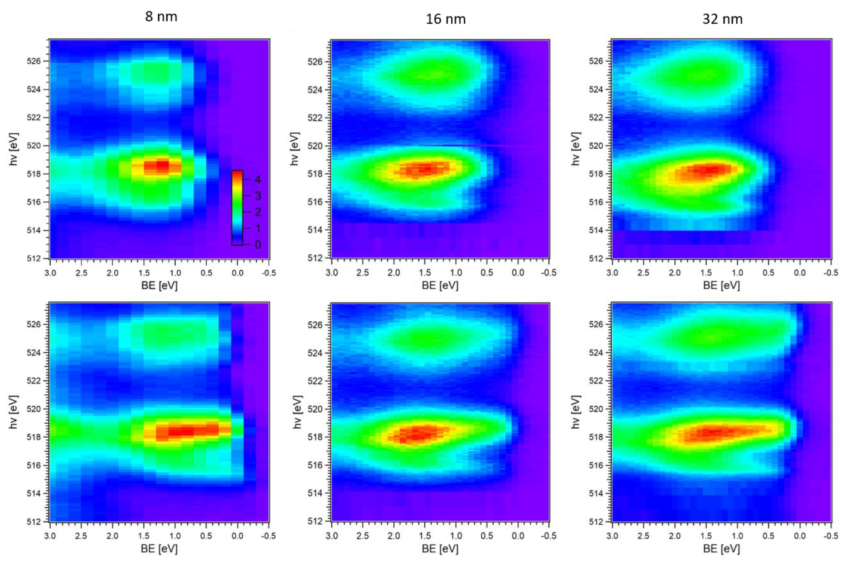
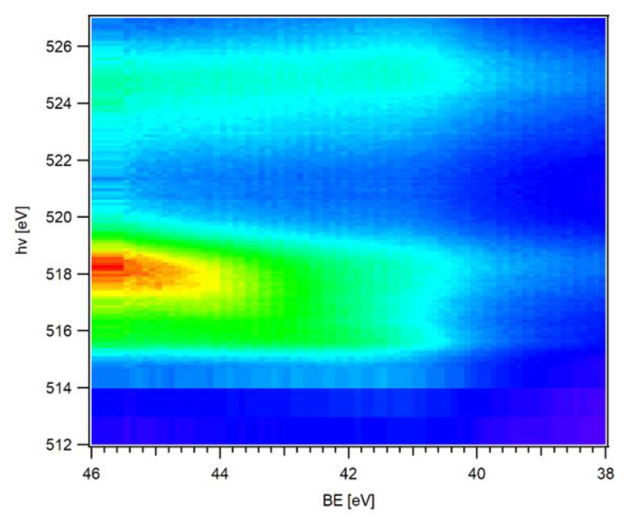
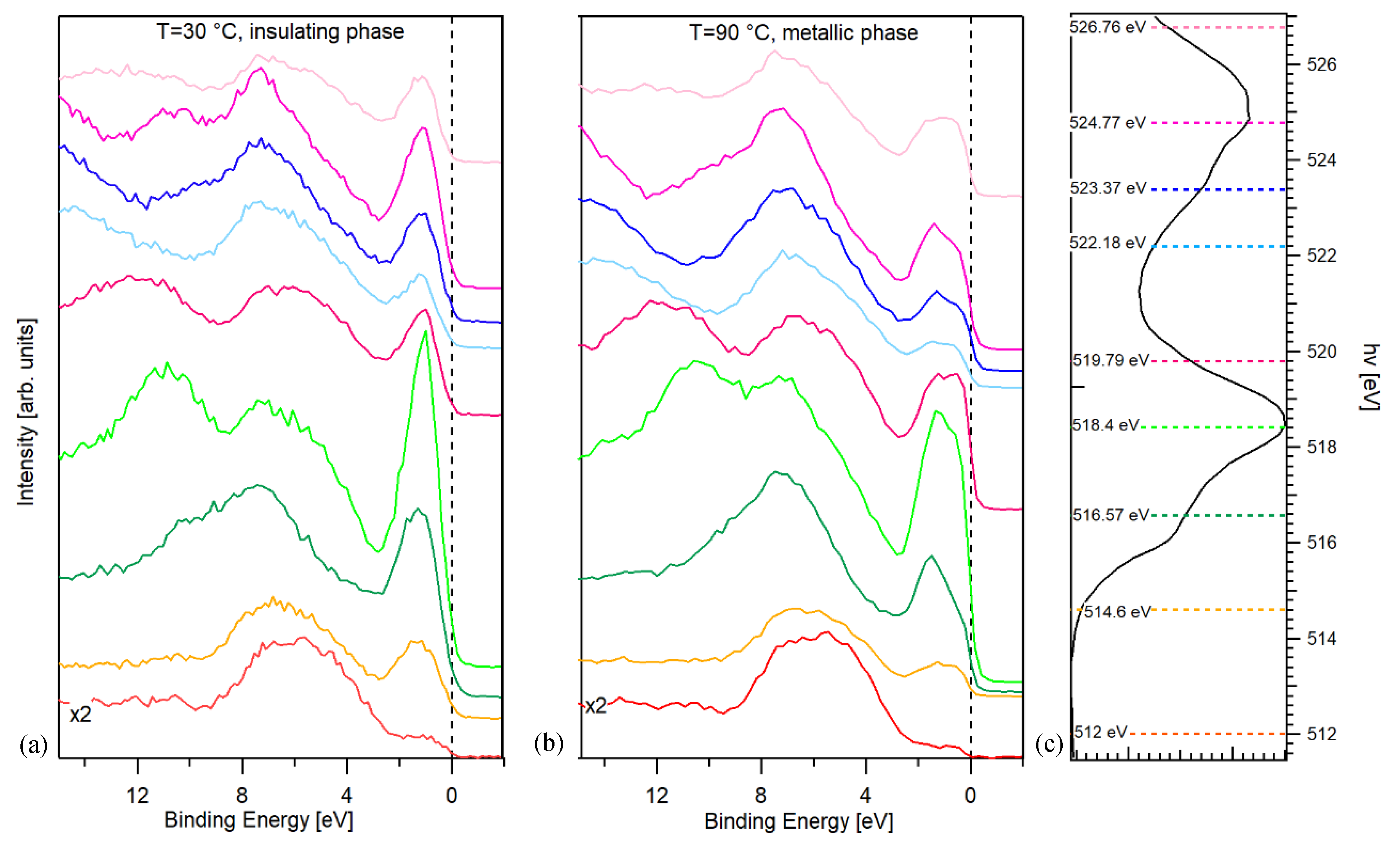
2.1. V 3d CIS Spectroscopy
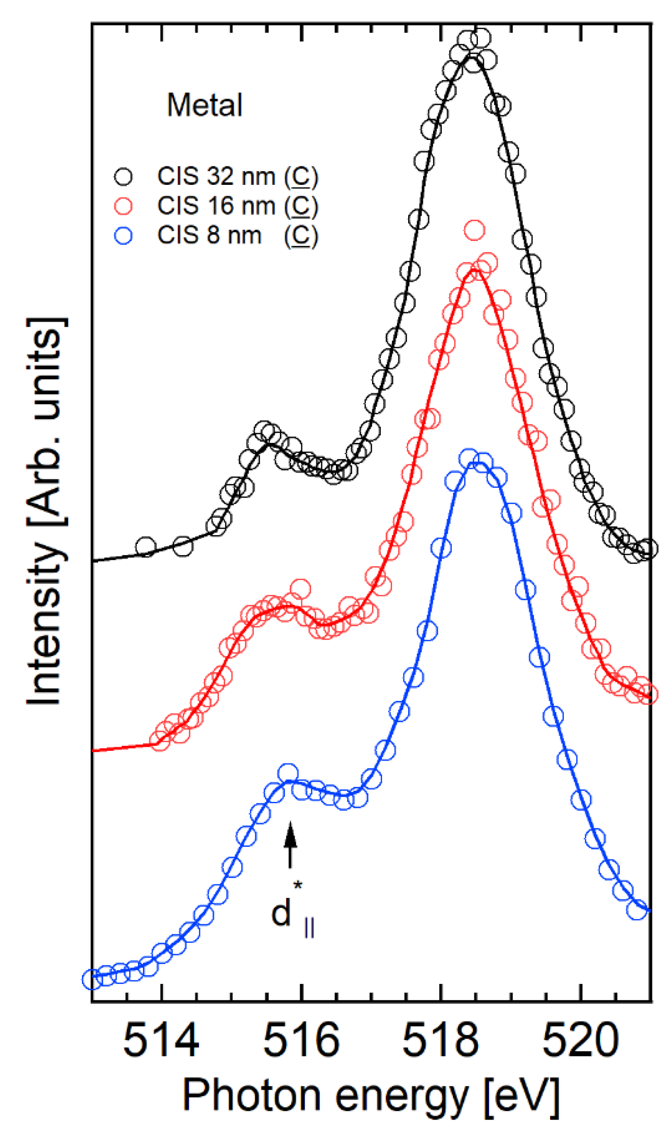
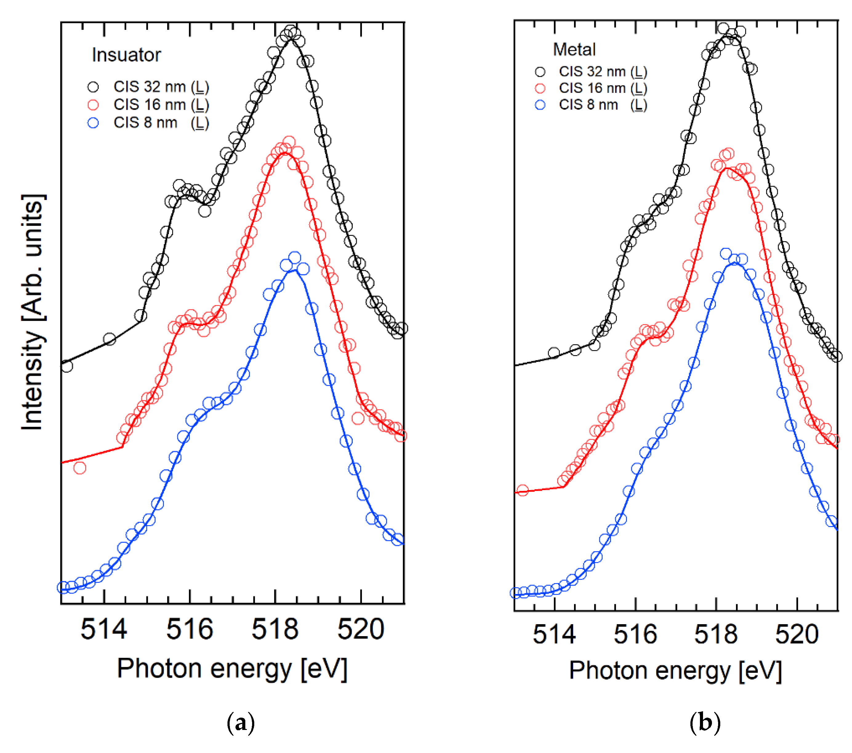
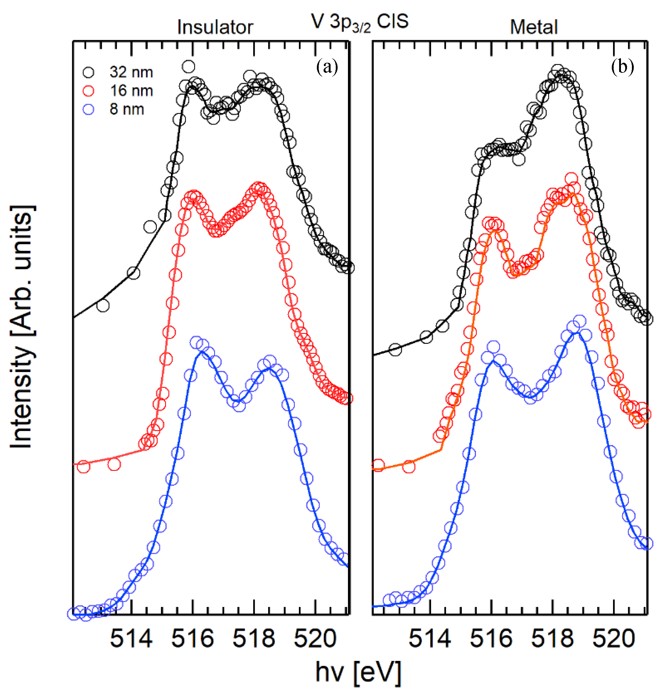
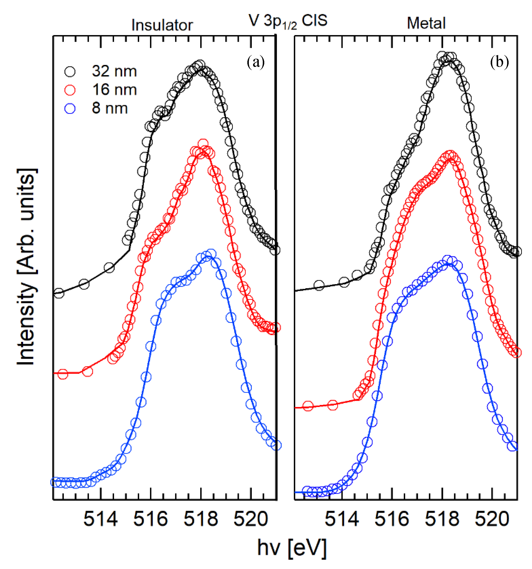
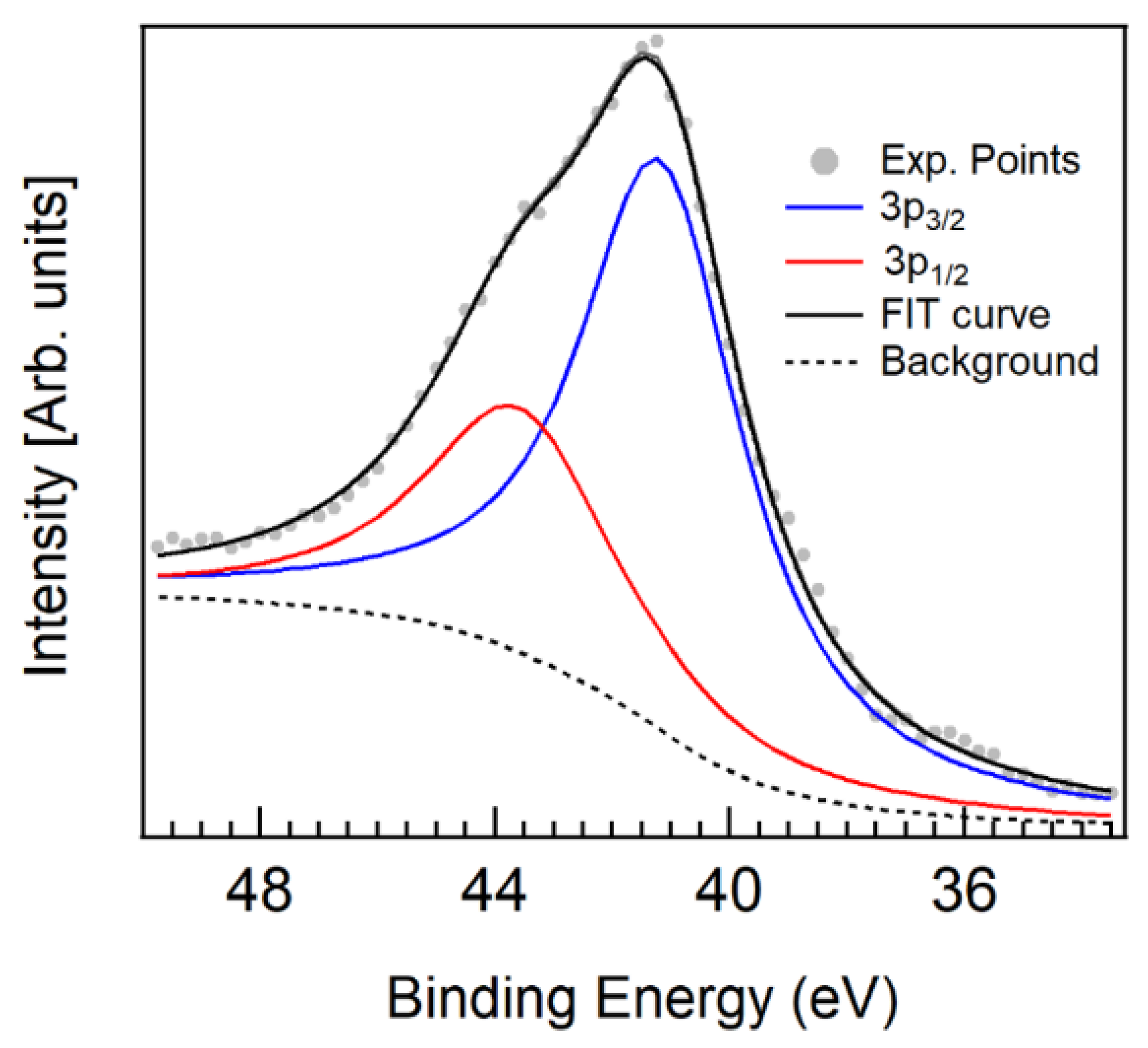
2.2. V 3p CIS Spectroscopy
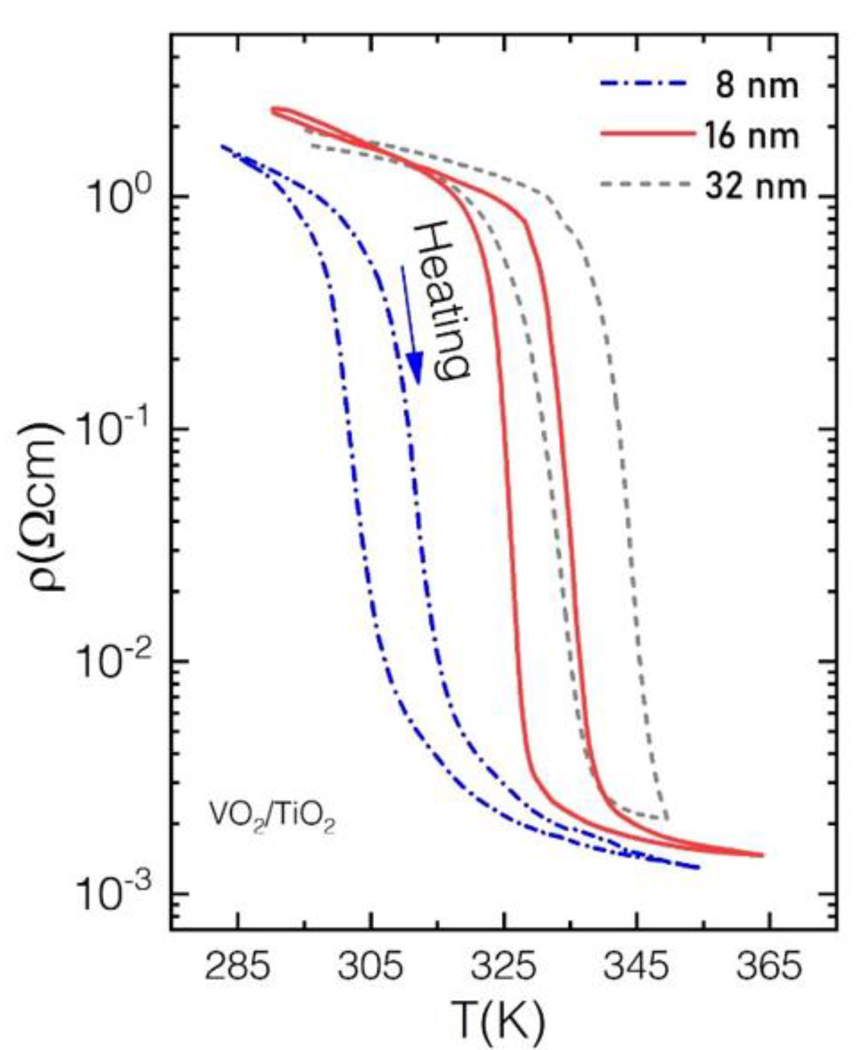
3. Discussion
4. Materials and Methods
Author Contributions
Funding
Conflicts of Interest
Appendix A

Appendix B


References
- Morin, F.J. Oxides which show a metal-to-insulator transition at the neel temperature. Phys. Rev. Lett. 1959, 3, 34–36. [Google Scholar] [CrossRef]
- Cui, Y.; Ke, Y.; Liu, C.; Chen, Z.; Wang, N.; Zhang, L.; Zhou, Y.; Wang, S.; Gao, Y.; Long, Y. Thermochromic VO2 for Energy-Efficient Smart Windows. Joule 2018, 2, 1707–1746. [Google Scholar] [CrossRef] [Green Version]
- Chen, S.; Wang, Z.; Ren, H.; Chen, Y.; Yan, W.; Wang, C.; Li, B.; Jiang, J.; Zou, C. Gate-controlled VO 2 phase transition for high-performance smart windows. Sci. Adv. 2019, 5, eaav6815. [Google Scholar] [CrossRef] [Green Version]
- Kang, C.; Zhang, C.; Yao, Y.; Yang, Y.; Zong, H.; Zhang, L.; Li, M. Enhanced thermochromic properties of vanadium dioxide (VO2)/glass heterostructure by inserting a Zr-based thin film metallic glasses (Cu50Zr50) buffer layer. Appl. Sci. 2018, 8, 1751. [Google Scholar] [CrossRef] [Green Version]
- Lin, J.; Ramanathan, S.; Guha, S. Electrically driven insulator-metal transition-based devices—Part I: The Electrothermal model and experimental analysis for the dc characteristics. IEEE Trans. Electron. Devices 2018, 65, 3982–3988. [Google Scholar] [CrossRef]
- Ramanathan, S. Thin Film Metal-Oxides: Fundamentals and Applications in Electronics and Energy; Springer: Boston, MA, USA, 2010; ISBN 9781441906632. [Google Scholar]
- Brahlek, M.; Zhang, L.; Lapano, J.; Zhang, H.T.; Engel-Herbert, R.; Shukla, N.; Datta, S.; Paik, H.; Schlom, D.G. Opportunities in vanadium-based strongly correlated electron systems. MRS Commun. 2017, 7, 27–52. [Google Scholar] [CrossRef] [Green Version]
- Koethe, T.C.; Hu, Z.; Haverkort, M.W.; Schüßler-Langeheine, C.; Venturini, F.; Brookes, N.B.; Tjernberg, O.; Reichelt, W.; Hsieh, H.H.; Lin, H.J.; et al. Transfer of spectral weight and symmetry across the metal-insulator transition in VO2. Phys. Rev. Lett. 2006. [Google Scholar] [CrossRef]
- D’Elia, A.; Grazioli, C.; Cossaro, A.; Li, B.W.; Zou, C.W.; Rezvani, S.J.; Pinto, N.; Marcelli, A.; Coreno, M. Strain mediated Filling Control nature of the Metal-Insulator Transition of VO2 and electron correlation effects in Nanostructured films. Appl. Surf. Sci. 2020, 148341. [Google Scholar] [CrossRef]
- Weber, C.; O’Regan, D.D.; Hine, N.D.M.; Payne, M.C.; Kotliar, G.; Littlewood, P.B. Vanadium Dioxide: A Peierls-Mott Insulator Stable against Disorder. Phys. Rev. Lett. 2012, 108, 256402. [Google Scholar] [CrossRef] [Green Version]
- Fan, L.L.; Chen, S.; Luo, Z.L.; Liu, Q.H.; Wu, Y.F.; Song, L.; Ji, D.X.; Wang, P.; Chu, W.S.; Gao, C.; et al. Strain dynamics of ultrathin VO2 film grown on TiO2 (001) and the associated phase transition modulation. Nano Lett. 2014, 14, 4036–4043. [Google Scholar] [CrossRef]
- Singh, C.N.; Piper, L.F.J.; Paik, H.; Schlom, D.G.; Lee, W. Correlation induced emergent charge order in metallic vanadium dioxide. arXiv 2020, arXiv:2005.02957. [Google Scholar]
- Aetukuri, N.B.; Gray, A.X.; Drouard, M.; Cossale, M.; Gao, L.; Reid, A.H.; Kukreja, R.; Ohldag, H.; Jenkins, C.A.; Arenholz, E.; et al. Control of the metal-insulator transition in vanadium dioxide by modifying orbital occupancy. Nat. Phys. 2013, 9, 661–666. [Google Scholar] [CrossRef]
- Park, J.H.; Coy, J.M.; Kasirga, T.S.; Huang, C.; Fei, Z.; Hunter, S.; Cobden, D.H. Measurement of a solid-state triple point at the metal–insulator transition in VO2. Nature 2013, 500, 431–434. [Google Scholar] [CrossRef]
- Narayan, J.; Bhosle, V.M. Phase transition and critical issues in structure-property correlations of vanadium oxide. J. Appl. Phys. 2006, 100. [Google Scholar] [CrossRef]
- Atkin, J.M.; Berweger, S.; Chavez, E.K.; Raschke, M.B.; Cao, J.; Fan, W.; Wu, J. Strain and temperature dependence of the insulating phases of VO2 near the metal-insulator transition. Phys. Rev. B Condens. Matter Mater. Phys. 2012, 85, 020101. [Google Scholar] [CrossRef] [Green Version]
- D’Elia, A.; Rezvani, S.J.; Cossaro, A.; Stredansky, M.; Grazioli, C.; Li, B.W.; Zou, C.W.; Coreno, M.; Marcelli, A. Strain Induced Orbital Dynamics Across the Metal Insulator Transition in Thin VO2/TiO2 (001) Films. J. Supercond. Nov. Magn. 2020, 33, 2383–2388. [Google Scholar] [CrossRef] [Green Version]
- Lopez, R.; Haynes, T.E.; Boatner, L.A.; Feldman, L.C.; Haglund, R.F. Size effects in the structural phase transition of VO2 nanoparticles. Phys. Rev. B Condens. Matter Mater. Phys. 2002, 65, 2241131–2241135. [Google Scholar] [CrossRef]
- Donev, E.U.; Ziegler, J.I.; Haglund, R.F.; Feldman, L.C. Size effects in the structural phase transition of VO2 nanoparticles studied by surface-enhanced Raman scattering. J. Opt. A Pure Appl. Opt. 2009, 11, 125002. [Google Scholar] [CrossRef]
- Fan, L.; Wang, F.; Chen, X.; Liu, Z.; Ma, C.; Zhu, L.; Meng, Q.; Wang, B.; Zhang, Q.; Zou, C. Well-Dispersed Monoclinic VO2 Nanoclusters with Uniform Size for Sensitive near-Infrared Detection. ACS Appl. Nano Mater. 2018, 1, 5044–5052. [Google Scholar] [CrossRef]
- Bachrach, R.Z. Synchrotron Radiation Research Advances in Surface and Interface Science; Bachrach, R.Z., Ed.; Springer: Boston, MA, USA, 1992; ISBN 978-0-306-43873-8. [Google Scholar]
- Marcelli, A.; Coreno, M.; Stredansky, M.; Xu, W.; Zou, C.; Fan, L.; Chu, W.; Wei, S.; Cossaro, A.; Ricci, A.; et al. Nanoscale Phase Separation and Lattice Complexity in VO2: The Metal–Insulator Transition Investigated by XANES via Auger Electron Yield at the Vanadium L23-Edge and Resonant Photoemission. Condens. Matter 2017, 2, 38. [Google Scholar] [CrossRef] [Green Version]
- Wu, M.; Zheng, J.C.; Wang, H.Q. Investigation of the vanadium L23 -edge X-ray absorption spectrum of SrVO3 using configuration interaction calculations: Multiplet, valence, and crystal-field effects. Phys. Rev. B 2018, 97, 245138. [Google Scholar] [CrossRef]
- Quackenbush, N.F.; Paik, H.; Wahila, M.J.; Sallis, S.; Holtz, M.E.; Huang, X.; Ganose, A.; Morgan, B.J.; Scanlon, D.O.; Gu, Y.; et al. Stability of the M2 phase of vanadium dioxide induced by coherent epitaxial strain. Phys. Rev. B 2016, 94, 085105. [Google Scholar] [CrossRef] [Green Version]
- Paez, G.J.; Singh, C.N.; Wahila, M.J.; Tirpak, K.E.; Quackenbush, N.F.; Sallis, S.; Paik, H.; Liang, Y.; Schlom, D.G.; Lee, T.L.; et al. Simultaneous Structural and Electronic Transitions in Epitaxial VO2/TiO2 (001). Phys. Rev. Lett. 2020, 124, 196402. [Google Scholar] [CrossRef]
- Bianconi, A. Multiplet splitting of final-state configurations in x-ray-absorption spectrum of metal VO2: Effect of core-hole-screening, electron correlation, and metal-insulator transition. Phys. Rev. B 1982, 26, 2741–2747. [Google Scholar] [CrossRef]
- Pinto, N.; Rezvani, S.J.; Favre, L.; Berbezier, I.; Fretto, M.; Boarino, L. Geometrically induced electron-electron interaction in semiconductor nanowires. Appl. Phys. Lett. 2016, 109, 123101. [Google Scholar] [CrossRef]
- Rezvani, S.J.; Gunnella, R.; Neilson, D.; Boarino, L.; Croin, L.; Aprile, G.; Fretto, M.; Rizzi, P.; Antonioli, D.; Pinto, N. Effect of carrier tunneling on the structure of Si nanowires fabricated by metal assisted etching. Nanotechnology 2016, 27, 345301. [Google Scholar] [CrossRef]
- Pasqualini, M.; Calcaterra, S.; Maroni, F.; Rezvani, S.J.; Di Cicco, A.; Alexander, S.; Rajantie, H.; Tossici, R.; Nobili, F. Electrochemical and spectroscopic characterization of an alumina-coated LiMn2O4 cathode with enhanced interfacial stability. Electrochim. Acta 2017, 258, 175–181. [Google Scholar] [CrossRef]
- Javad Rezvani, S.; Di Gioacchino, D.; Gatti, C.; Ligi, C.; Guidi, M.C.; Cibella, S.; Fretto, M.; Poccia, N.; Lupi, S.; Marcelli, A. Proximity array device: A novel photon detector working in long wavelengths. Condens. Matter 2020, 5, 33. [Google Scholar] [CrossRef]
- D’Elia, A.; Cepek, C.; de Simone, M.; Macis, S.; Belec, B.; Fanetti, M.; Piseri, P.; Marcelli, A.; Coreno, M. Interplay among work function, electronic structure and stoichiometry in nanostructured VO x films. Phys. Chem. Chem. Phys. 2020, 22, 6282–6290. [Google Scholar] [CrossRef] [Green Version]
- Mossanek, R.J.O.; Abbate, M. Cluster model calculations with nonlocal screening channels of metallic and insulating VO2. Phys. Rev. B Condens. Matter Mater. Phys. 2006, 74, 125112. [Google Scholar] [CrossRef] [Green Version]
- Lapeyre, G.J.; Smith, R.J.; Knapp, J.; Anderson, J. Constant Final Energy and Constant Initial Energy Spectroscopy. Le J. Phys. Colloq. 1978, 39, 134–141. [Google Scholar] [CrossRef]
- Solomon, E.I.; Basumallick, L.; Chen, P.; Kennepohl, P. Variable energy photoelectron spectroscopy: Electronic structure and electronic relaxation. Coord. Chem. Rev. 2005, 249, 229–253. [Google Scholar] [CrossRef]
- D’Elia, A.; Grazioli, C.; Cossaro, A.; Li, B.; Zou, C.; Rezvani, J.; Pinto, N.; Marcelli, A.; Coreno, M. Electron Correlation driven Metal-Insulator transition in Strained and Disordered VO2 films. arXiv 2020, arXiv:2006.07930. [Google Scholar]
- De Groot, F. Multiplet effects in X-ray spectroscopy. Coord. Chem. Rev. 2005, 249, 31–63. [Google Scholar] [CrossRef]
- Goodenough, J.B. The two components of the crystallographic transition in VO2. J. Solid State Chem. 1971, 3, 490–500. [Google Scholar] [CrossRef]
- Sawatzky, G.A.; Post, D. X-ray photoelectron and Auger spectroscopy study of some vanadium oxides. Phys. Rev. B 1979, 20, 1546–1555. [Google Scholar] [CrossRef]
- Ruzmetov, D.; Senanayake, S.D.; Ramanathan, S. X-ray absorption spectroscopy of vanadium dioxide thin films across the phase-transition boundary. Phys. Rev. B Condens. Matter Mater. Phys. 2007, 75. [Google Scholar] [CrossRef] [Green Version]
- Cavalleri, A.; Dekorsy, T.; Chong, H.H.W.; Kieffer, J.C.; Schoenlein, R.W. Evidence for a structurally-driven insulator-to-metal transition in VO2: A view from the ultrafast timescale. Phys. Rev. B 2004, 70, 161102. [Google Scholar] [CrossRef] [Green Version]
- Schmid, M.; Steinrück, H.P.; Gottfried, J.M. A new asymmetric Pseudo-Voigt function for more efficient fitting of XPS lines. Surf. Interface Anal. 2014, 46, 505–511. [Google Scholar] [CrossRef]
- Zimmermann, R.; Claessen, R.; Reinert, F.; Steiner, P.; Hüfner, S. Strong hybridization in vanadium oxides: Evidence from photoemission and absorption spectroscopy. J. Phys. Condens. Matter 1998, 10, 5697–5716. [Google Scholar] [CrossRef]
- Lytken, O.; Wechsler, D.; Steinrück, H.P. Removing photoemission features from Auger-yield NEXAFS spectra. J. Electron Spectros. Relat. Phenom. 2017. [Google Scholar] [CrossRef]
- Lee, S.; Meyer, T.L.; Sohn, C.; Lee, D.; Nichols, J.; Lee, D.; Seo, S.S.A.; Freeland, J.W.; Noh, T.W.; Lee, H.N. Electronic structure and insulating gap in epitaxial VO2 polymorphs. APL Mater. 2015, 3, 126109. [Google Scholar] [CrossRef] [Green Version]
- Fan, L.L.; Chen, S.; Wu, Y.F.; Chen, F.H.; Chu, W.S.; Chen, X.; Zou, C.W.; Wu, Z.Y. Growth and phase transition characteristics of pure M-phase VO2 epitaxial film prepared by oxide molecular beam epitaxy. Appl. Phys. Lett. 2013, 103. [Google Scholar] [CrossRef]
- Costantini, R.; Stredansky, M.; Cvetko, D.; Kladnik, G.; Verdini, A.; Sigalotti, P.; Cilento, F.; Salvador, F.; De Luisa, A.; Benedetti, D.; et al. ANCHOR-SUNDYN: A novel endstation for time resolved spectroscopy at the ALOISA beamline. J. Electron Spectros. Relat. Phenom. 2018, 229, 7–12. [Google Scholar] [CrossRef]


Publisher’s Note: MDPI stays neutral with regard to jurisdictional claims in published maps and institutional affiliations. |
© 2020 by the authors. Licensee MDPI, Basel, Switzerland. This article is an open access article distributed under the terms and conditions of the Creative Commons Attribution (CC BY) license (http://creativecommons.org/licenses/by/4.0/).
Share and Cite
D’Elia, A.; Grazioli, C.; Cossaro, A.; Li, B.; Zou, C.; Rezvani, S.J.; Marcelli, A.; Coreno, M. Detection of Spin Polarized Band in VO2/TiO2(001) Strained Films via Orbital Selective Constant Initial State Spectroscopy. Condens. Matter 2020, 5, 72. https://0-doi-org.brum.beds.ac.uk/10.3390/condmat5040072
D’Elia A, Grazioli C, Cossaro A, Li B, Zou C, Rezvani SJ, Marcelli A, Coreno M. Detection of Spin Polarized Band in VO2/TiO2(001) Strained Films via Orbital Selective Constant Initial State Spectroscopy. Condensed Matter. 2020; 5(4):72. https://0-doi-org.brum.beds.ac.uk/10.3390/condmat5040072
Chicago/Turabian StyleD’Elia, Alessandro, Cesare Grazioli, Albano Cossaro, Bowen Li, Chongwen Zou, Seyed Javad Rezvani, Augusto Marcelli, and Marcello Coreno. 2020. "Detection of Spin Polarized Band in VO2/TiO2(001) Strained Films via Orbital Selective Constant Initial State Spectroscopy" Condensed Matter 5, no. 4: 72. https://0-doi-org.brum.beds.ac.uk/10.3390/condmat5040072