
Chalcogen Atom-Doped Graphene and Its Performance in N2 Activation


1
Department of Materials, Imperial College London, London SW7 2AZ, UK
2
Faculty of Engineering, Environment and Computing, Coventry University, Priory Street, Coventry CV1 5FB, UK
Surfaces 2022, 5(2), 228-237; https://0-doi-org.brum.beds.ac.uk/10.3390/surfaces5020016
Submission received: 28 December 2021
/
Revised: 7 March 2022
/
Accepted: 8 March 2022
/
Published: 1 April 2022
Abstract
:In this work, we studied dispersion correction, adsorption and substitution of chalcogen dopants (O, S, Se and Te) on the surface of graphene using density functional theory. The results reveal that a single oxygen atom is more preferred for adsorption onto the graphene surface than the other dopants, with an adsorption energy of −0.84 eV. The preference of this dopant is evidenced by a greater charge transfer of 0.34 electrons from the graphene surface to the oxygen. The substitutional doping of oxygen is energetically more favourable than the doping of other atoms. While nitrogen activation is enhanced by the adsorption, the activation is not significant with the doping of chalcogen atoms.
1. Introduction
Graphene is one of the allotropes of carbon, consisting of a two-dimensional mono layer of carbon atoms with sp2 hybridization [1,2,3,4]. Due to its remarkable mechanical, thermal, chemical and electrical properties, graphene is considered to be a versatile material with many applications in areas such as electronics, optics and energy storage systems [5,6,7,8,9,10,11,12,13].
The doping of graphene with hetero atoms (n-type or p-type impurities) has been shown to be an efficient way of altering its electrochemical performance and electronic properties [14,15,16,17]. The doping of B led to a significant charge transfer, and a negatively charged graphene surface was identified as a host material for adsorbing pollutants such as heavy metals [18,19,20,21]. Si-doped graphene has many potential applications, including serving as a catalyst for the reduction of CO2 [22,23,24]. Using N-doped graphene, significant improvement has been achieved in the properties of fuel cells, Li-ion batteries and super capacitors [25,26,27].
Non-metal dopants such as S, P, F and I are reported to be promising catalysts for oxygen reduction reactions [28,29,30,31,32]. While there are many experimental studies available in the literature on doped graphene, a significant amount of theoretical work based on density functional theory (DFT) has also been reported [33,34,35,36].
In this study, we use spin-polarized DFT together with dispersion correction to examine the structures of chalcogen atoms (O, S, Se and Te) adsorbed and substitutionally doped graphene surfaces. Furthermore, activation of nitrogen molecules on the surfaces of adsorbed and doped graphene is studied.
2. Computational Methods
All calculations were performed using a plane wave DFT simulation code VASP (Vienna ab initio simulation program) [37]. Kohn–Sham (KS) equations are solved using plane wave basis sets and projected augmented wave (PAW) potentials [38]. A plane wave basis set with a cut-off of 500 eV was used in all calculations. The generalized gradient approximation (GGA) as formulated by Perdew, Burke and Ernzerhof (PBE) [39] was used to describe the exchange-correlation term. All structures were relaxed with the aid of a conjugate gradient algorithm [40]. In all relaxed configurations, forces on the atoms were smaller than 0.001 eV/Å. A supercell with dimensions of 25.5 Å × 14.75 Å × 30 Å was used to ensure that adjacent dopants or molecules do not interact each other. A 4 × 4 × 1 Monk-horst [41] k-point mesh was used to optimize all configurations. Bulk diamond and graphite were optimized using 8 × 8 × 8 and 8 × 8 × 4 k point meshes, respectively. A semi-empirical method describing dispersive interactions was used as modelled by Grimme et al. [42]. Bader charge analysis [43] was used to calculate the charges on the dopants and C atoms on the graphene. Adsorption energy of a molecular nitrogen interacting with the atoms adsorbed or doped graphene surface was calculated using the following equation:
where is the total energy of a molecular nitrogen adsorbed or doped on the surface of metal doped on the graphene surface, is the total energy of a metal-doped graphene surface and is the total energy of molecular nitrogen.
3. Results
3.1. Validation of Simulation Parameters
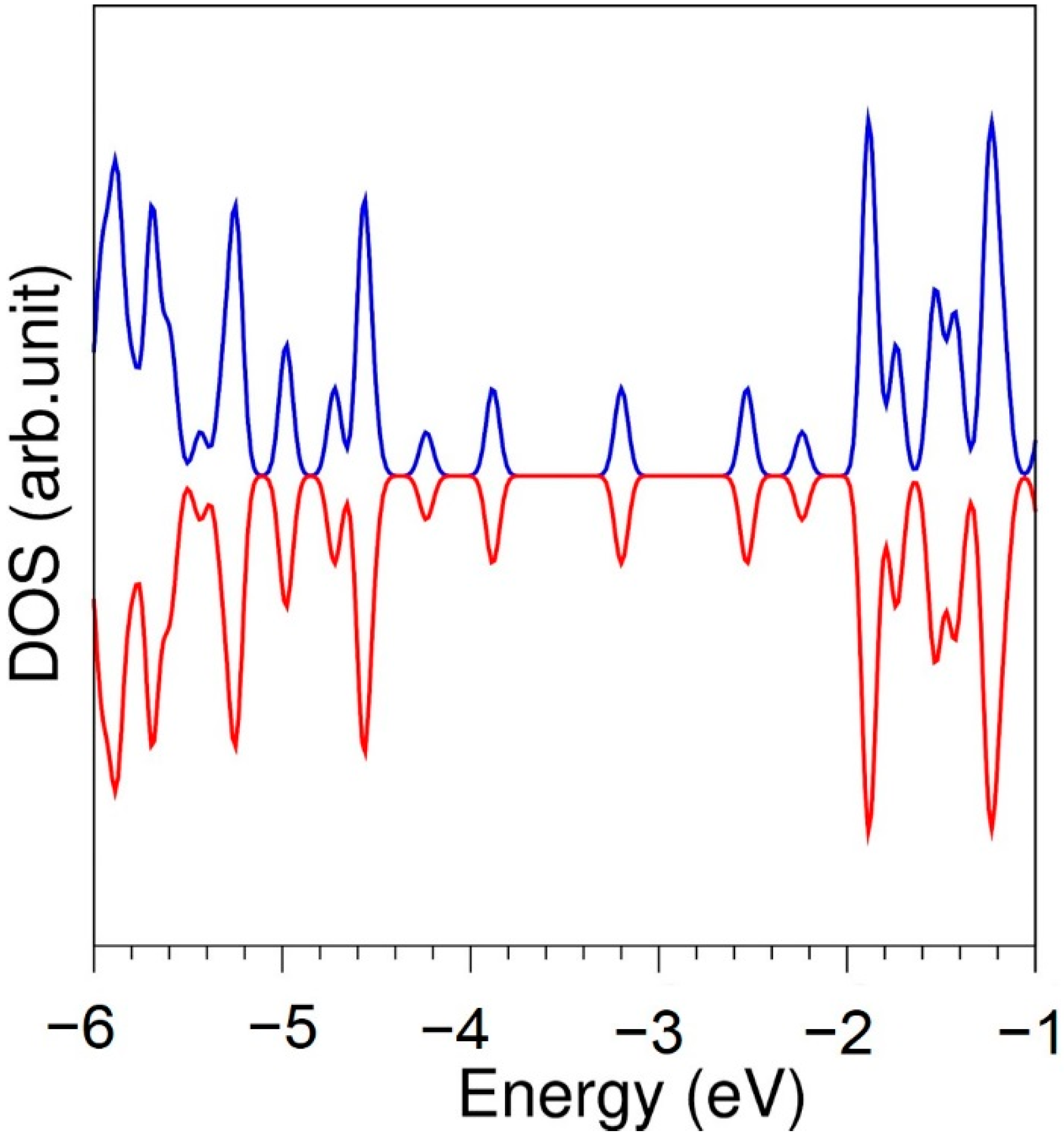
First, we performed full geometry optimization calculations on diamond, graphite, bulk S8, bulk Se and bulk Te to obtain equilibrium lattice constants and compare them with corresponding experimental values [44,45,46,47,48] (see Table 1). There is good agreement between experimental and calculated values, showing the efficacy of the PAW potentials used in this study. In Figure 1, the density of states (DOS) is shown. Graphene is a semiconductor as reported in previous studies [49], in agreement with the present simulation.
3.2. Adsorption of N2 on the Graphene
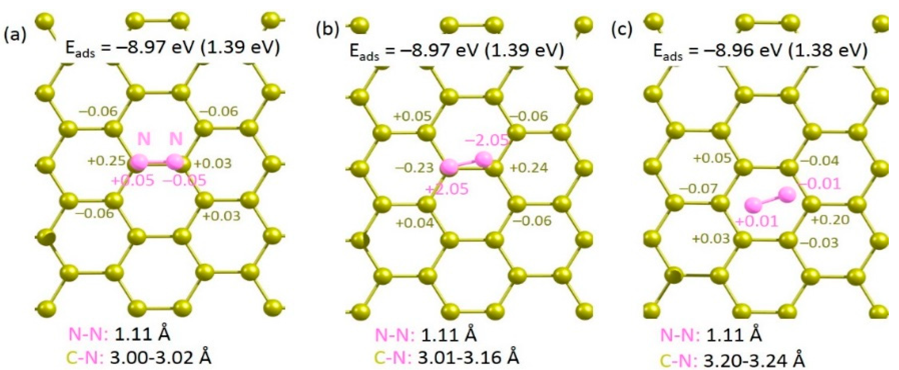
A single nitrogen molecule was allowed to adsorb on the surface of pristine graphene. Three different configurations were considered (see Figure 2). In all cases, adsorption is endoergic with respect to the N2 molecule, indicating that the molecule is more stable in the gas phase than on the graphene surface. This is evidenced by the longer C-N bond distances (3.00–3.10 Å). Furthermore, Bader charges on the N2 molecules show that there is no charge transfer between N2 molecule and graphene. However, both the N2 molecule and graphene surface are slightly polarized. Exoergic adsorption energies are calculated in all cases with respect to the gas phase N atom. This is due to the exothermic formation energy of the N2 molecule from gas phase N atoms.
3.3. Adsorption of N2 on the Graphene Adsorbed with O, S, Se and Te
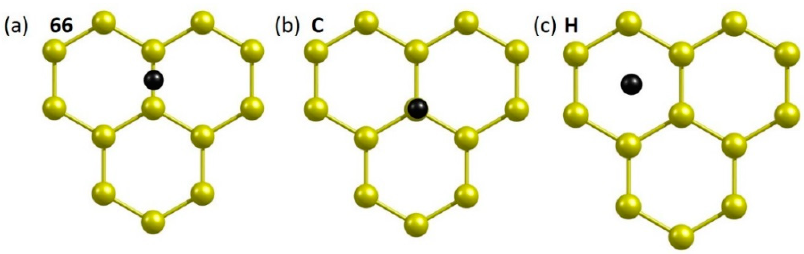
Next, chalcogen dopants were allowed to interact with pristine graphene. Three different initial configurations (66, C and H) were considered (see Figure 3). In configuration 66, the dopant atom is on the top of the C-C bond. The atom is on the top of a carbon in configuration C. In configuration H, the top of a hexagonal ring is occupied by a dopant atom. All initial configurations were allowed to relax. The relative energies of all dopants with respect to their most stable configuration (66) are shown in Table 2.
The results show that the most favourable position for all dopants is the 66 position (see Table 2). Other configurations exhibit slightly higher energy.
Relaxed structures showing the chalcogen atoms adsorbing on the 66 position of graphene is given in Figure 4a–d. Charge density plots associated with the interaction of dopant atoms with graphene are shown in Figure 4e–f.
Table 3 reports the adsorption energies, Bader charges on the dopants and C-X bond distances in the most stable (66) configurations. In all cases, adsorption is exothermic, meaning that adsorbed configurations are stable. The strongest adsorption is due to the highest electron negativity of O (3.44) compared to other dopants [50]. This is further confirmed by the most negative Bader charge on O and the shortest C-O bond distance. Adsorption decreases with decreasing electronegativity, decreasing Bader charge and increasing C-X bond distance (see Figure 4).
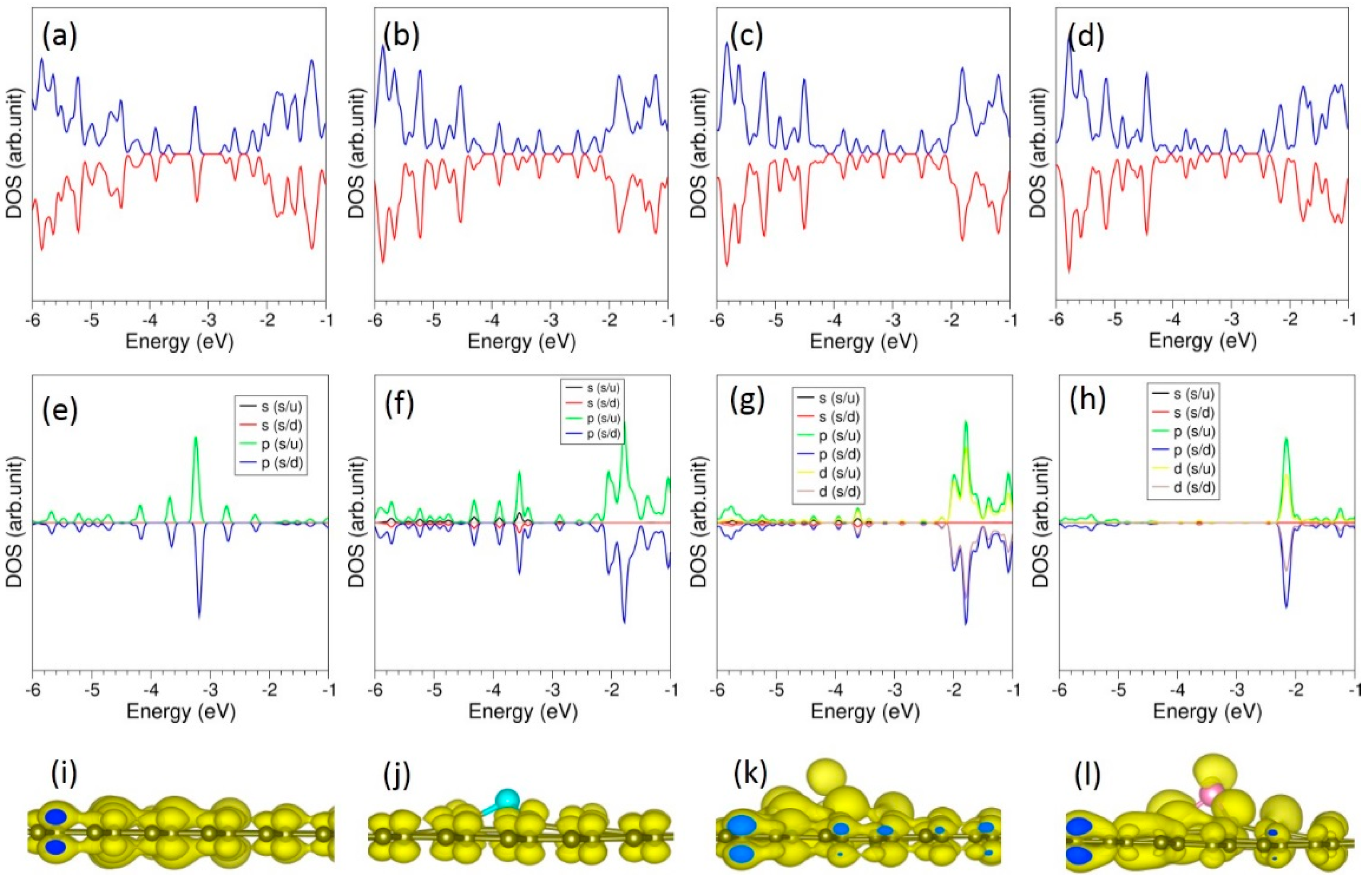
All doped configurations are still semiconductos (see Figure 5). However, p-states of dopant atoms are dispersed in the gap and the top of the valence band.
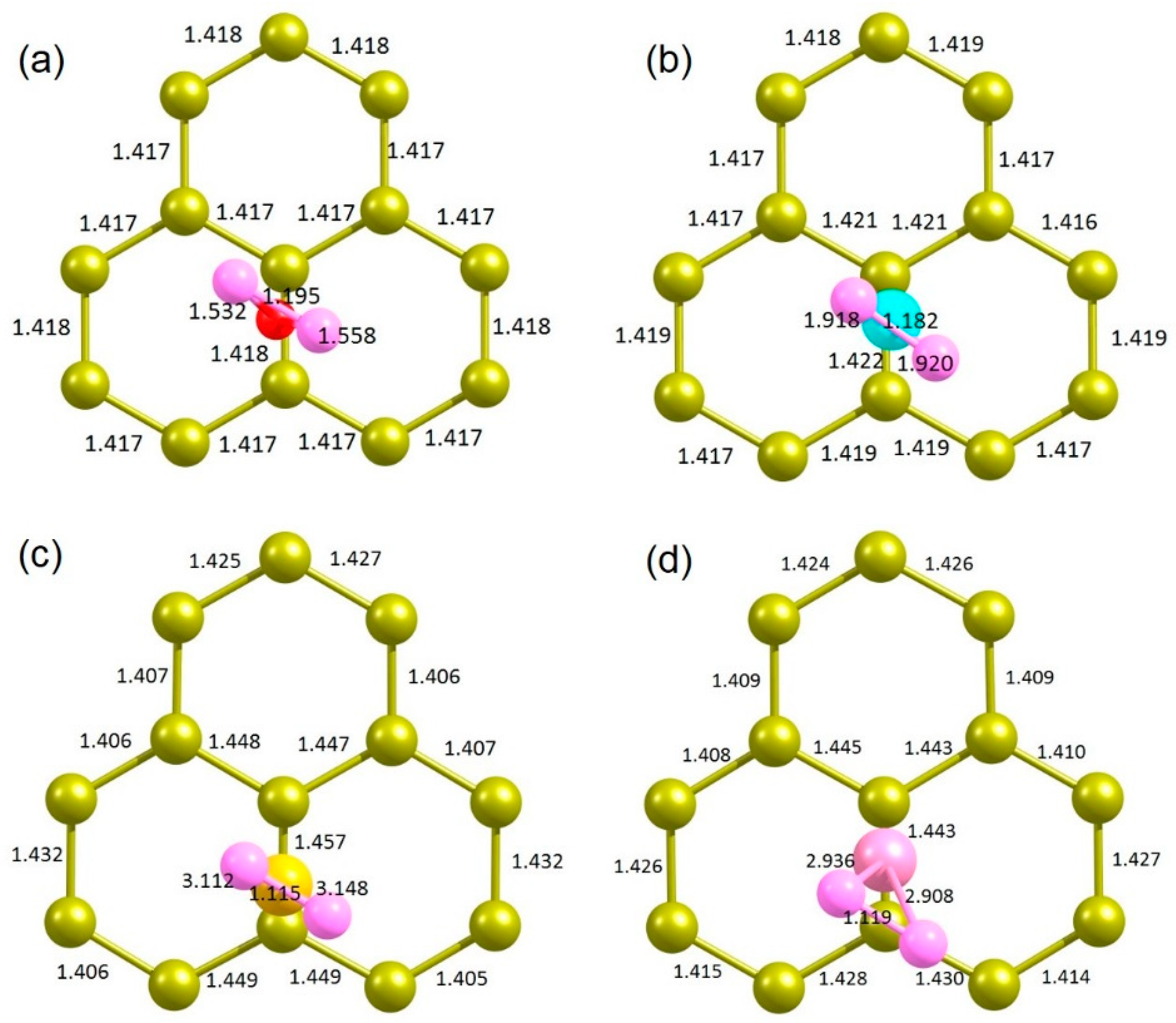
Interaction of the N2 molecule on the surface of atoms adsorbed onto graphene is next considered next. Relaxed structures are shown in Figure 6. Table 4 reports the adsorption energies, Bader charges on N2 and adsorbed atoms, and the shortest bond distances. Calculations show that adsorption energies are positive, meaning that adsorption is unfavourable. Lower positive adsorption energies are calculated for O and S. This is reflected in the shorter O-N and S-N bond distances. In the case of Se and Te, Se-N and Te-N bond distances are longer than the O-N and S-N bond distances. This is reflected in the larger positive adsorption energies.
In the case of O and S, N-N bond distances are elongated significantly compared to that calculated for the gas phase N2 molecule (1.10 Å). Activation of N ≡ N is very small for Se and Te.
3.4. Doping of O, S, Se and Te
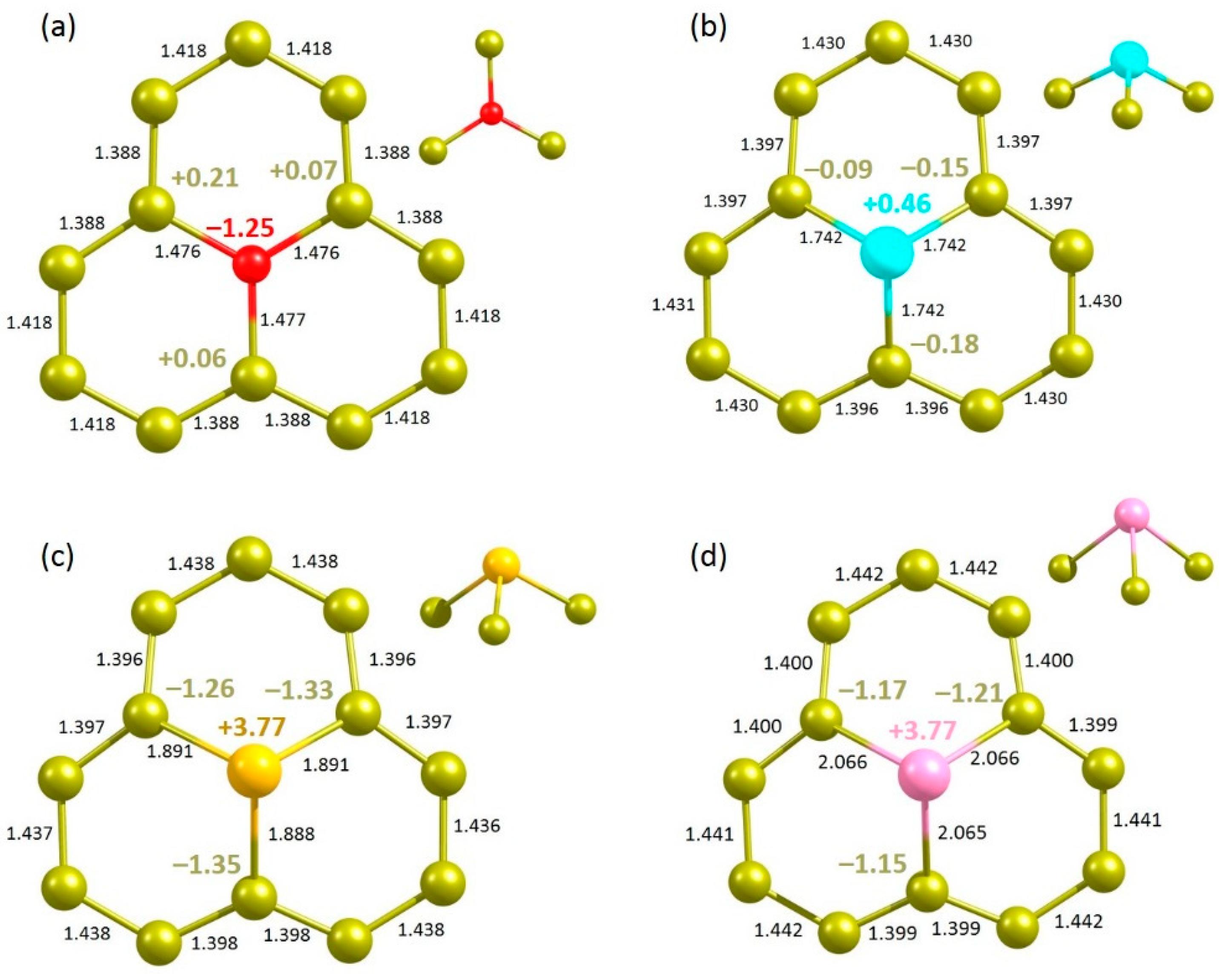
Next, we considered the substitutional doping of chalcogen dopant atoms to enhance the degree of adsorption. Figure 7 shows the relaxed structures. The doped O forms a trigonal planar structure. The calculated substitution energy of O is 7.43 eV (Table 5). This indicates that the C-O bond is weaker than the C-C bond, as evidenced by the longer C–O bond length. This is partly due to the higher electronegativity of O than that of C. In the defect-free graphene, the C-C bond length is 1.41 Å. The C-O bond length is 0.06 Å longer than the C-C bond length in the pristine graphene (Figure 7a). The Bader charge analysis shows that the O atom gains 1.25 electrons from adjacent carbon atoms, leading to its higher electronegativity (3.44) than that of C (2.55) [50]. The valance band is occupied by the p states of O (see Figure 8a,e). Conversely, all other atoms form a trigonal pyramid structure in their relaxed structures (see Figure 7b–d). Substitution energy and C-X bond distance increase with increasing electronegativity. Bader charge analysis shows that there is a charge transfer from doped atoms to the nearest neighbour C atoms. Both S and Se exhibit similar +3.77 Bader charge, showing significant charge transfer. DOS plots show that p states of S, Se and Te are mainly occupied in the band gap region. Charge density plots show the electron distribution around the doped atoms and the nearest neighbour C atoms as observed in the Bader charge analysis.
DOS plots show that p states of S, Se and Te mainly occupy the band gap region (see Figure 8). Charge density plots show the electron distribution around the doped atoms and the nearest neighbour C atoms as observed in the Bader charge analysis.
3.5. N2 Adsorption onto the Surface of Doped Graphene
Finally, the doped surface structures were considered for the adsorption of chalcogen atoms. The relaxed structures are shown in Figure 9. In the case of doping with O, exoergic adsorption energy (−0.07 eV) is calculated (see Table 6). Other dopants exhibit endoergic adsorption energies. Activation of the N2 molecule is very small, as evidenced by the very small elongation in the N ≡ N bond length. A very large positive adsorption energy of 5.65 eV is calculated for Te, meaning that this dopant is highly unfavourable.
4. Conclusions
In this study, we report the structures and energetics of chalcogen atoms adsorbed and doped onto graphene using DFT simulations together with dispersion. We show that a single oxygen atom exhibits stronger adsorption than the other dopants. The adsorption energy is calculated to be −0.84 eV. Such strong adsorption is evidenced by the charge transfer (0.34 e) from the graphene surface to the oxygen. The most favourable atom for doping substitutionally on the surface is the oxygen. The adsorption enhances the nitrogen activation. Substitutional doping has no significant effect on nitrogen activation.
Funding
This research received no external funding.
Data Availability Statement
The data presented in this study are available upon reasonable request from the corresponding author.
Acknowledgments
High performance computing centre at Imperial College London is acknowledged for providing computational facilities.
Conflicts of Interest
The author declares no conflict of interest.
References
- Katsnelson, M.I. Graphene: Carbon in two dimensions. Mater. Today 2007, 10, 20–27. [Google Scholar] [CrossRef]
- Allen, M.J.; Tung, V.C.; Kaner, R.B. Honeycomb Carbon: A Review of Graphene. Chem. Rev. 2010, 110, 132–145. [Google Scholar] [CrossRef]
- Wu, Y.; Wang, S.; Komvopoulos, K. A review of graphene synthesis by indirect and direct deposition methods. J. Mater. Res. 2020, 35, 76–89. [Google Scholar] [CrossRef]
- Tiwari, S.K.; Sahoo, S.; Wang, N.; Huczko, A. Graphene research and their outputs: Status and prospect. J. Sci. Adv. Mater. Devices 2020, 5, 10–29. [Google Scholar] [CrossRef]
- Papageorgiou, D.G.; Kinloch, I.A.; Young, R.J. Mechanical properties of graphene and graphene-based nanocomposites. Prog. Mater. Sci. 2017, 90, 75–127. [Google Scholar] [CrossRef]
- Sang, M.; Shin, J.; Kim, K.; Yu, K.J. Electronic and Thermal Properties of Graphene and Recent Advances in Graphene Based Electronics Applications. Nanomaterials 2019, 9, 374. [Google Scholar] [CrossRef] [PubMed] [Green Version]
- Kim, Y.-J.; Kim, Y.; Novoselov, K.; Hong, B.H. Engineering electrical properties of graphene: Chemical approaches. 2D Mater. 2015, 2, 042001. [Google Scholar] [CrossRef]
- Lee, J.H.; Park, S.J.; Choi, J.W. Electrical Property of Graphene and Its Application to Electrochemical Biosensing. Nanomaterials 2019, 9, 297. [Google Scholar] [CrossRef] [Green Version]
- Olabi, A.G.; Abdelkareem, M.A.; Wilberforce, T.; Sayed, E.T. Application of graphene in energy storage device—A review. Renew. Sustain. Energy Rev. 2021, 135, 110026. [Google Scholar] [CrossRef]
- Syama, S.; Mohanan, P.V. Comprehensive Application of Graphene: Emphasis on Biomedical Concerns. Nano-Micro Lett. 2019, 11, 6. [Google Scholar] [CrossRef] [Green Version]
- Madurani, K.A.; Suprapto, S.; Machrita, N.I.; Bahar, S.L.; Illiya, W.; Kurniawan, F. Progress in Graphene Synthesis and its Application: History, Challenge and the Future Outlook for Research and Industry. ECS J. Solid State Sci. Technol. 2020, 9, 093013. [Google Scholar] [CrossRef]
- Dhinakaran, V.; Lavanya, M.; Vigneswari, K.; Ravichandran, M.; Vijayakumar, M.D. Review on exploration of graphene in diverse applications and its future horizon. Mater. Today Proc. 2020, 27, 824–828. [Google Scholar] [CrossRef]
- Zheng, W.; Zhao, X.; Fu, W. Review of Vertical Graphene and its Applications. ACS Appl. Mater. Interfaces 2021, 13, 9561–9579. [Google Scholar] [CrossRef]
- Chae, S.; Panomsuwan, G.; Bratescu, M.A.; Teshima, K.; Saito, N. p-Type Doping of Graphene with Cationic Nitrogen. ACS Appl. Nano Mater. 2019, 2, 1350–1355. [Google Scholar] [CrossRef]
- Liu, H.; Liu, Y.; Zhu, D. Chemical doping of graphene. J. Mater. Chem. 2011, 21, 3335–3345. [Google Scholar] [CrossRef]
- Meng, X.; Tongay, S.; Kang, J.; Chen, Z.; Wu, F.; Li, S.-S.; Xia, J.B.; Li, J.; Wu, J. Stable p- and n-type doping of few-layer graphene/graphite. Carbon 2013, 57, 507–514. [Google Scholar] [CrossRef]
- Du, J.; Duan, J.; Yang, X.; Duan, Y.; Zhou, Q.; Tang, Q. p-Type Charge Transfer Doping of Graphene Oxide with (NiCo)1−yFeyOx for Air-Stable, All-Inorganic CsPbIBr2 Perovskite Solar Cells. Angew. Chem. Int. Ed. 2021, 60, 10608–10613. [Google Scholar] [CrossRef] [PubMed]
- Feng, L.; Qin, Z.; Huang, Y.; Peng, K.; Wang, F.; Yan, Y.; Chen, Y. Boron-, sulfur-, and phosphorus-doped graphene for environmental applications. Sci. Total Environ. 2020, 698, 134239. [Google Scholar] [CrossRef]
- Han, J.; Zhang, L.L.; Lee, S.; Oh, J.; Lee, K.S.; Potts, J.R.; Ji, J.; Zhao, X.; Ruoff, R.S.; Park, S. Generation of B-Doped Graphene Nanoplatelets Using a Solution Process and Their Supercapacitor Applications. ACS Nano 2013, 7, 19–26. [Google Scholar] [CrossRef] [PubMed]
- Sahoo, M.; Sreena, K.P.; Vinayan, B.P.; Ramaprabhu, S. Green synthesis of boron doped graphene and its application as high performance anode material in Li ion battery. Mater. Res. Bull. 2015, 61, 383–390. [Google Scholar] [CrossRef]
- Wang, H.; Zhou, Y.; Wu, D.; Liao, L.; Zhao, S.; Peng, H.; Liu, Z. Synthesis of Boron-Doped Graphene Monolayers Using the Sole Solid Feedstock by Chemical Vapor Deposition. Small 2013, 9, 1316–1320. [Google Scholar] [CrossRef] [PubMed]
- Fang, L.; Cao, Z. CO2 activation at atomically dispersed Si sites of N-doped graphenes: Insight into distinct electron mechanisms from first-principles calculations. AIP Adv. 2021, 11, 115302. [Google Scholar] [CrossRef]
- Kuganathan, N.; Anurakavan, S.; Abiman, P.; Iyngaran, P.; Gkanas, E.I.; Chroneos, A. Adsorption of lead on the surfaces of pristine and B, Si and N-doped graphene. Phys. B Condens. Matter 2021, 600, 412639. [Google Scholar] [CrossRef]
- Chen, Y.; Liu, Y.J.; Wang, H.X.; Zhao, J.X.; Cai, Q.H.; Wang, X.Z.; Ding, Y.H. Silicon-Doped Graphene: An Effective and Metal-Free Catalyst for NO Reduction to N2O? ACS Appl. Mater. Interfaces 2013, 5, 5994–6000. [Google Scholar] [CrossRef]
- Su, H.; Hu, Y.H. Recent advances in graphene-based materials for fuel cell applications. Energy Sci. Engin. 2021, 9, 958–983. [Google Scholar] [CrossRef]
- Yoo, E.; Nakamura, J.; Zhou, H. N-Doped graphene nanosheets for Li–air fuel cells under acidic conditions. Energy Environ. Sci. 2012, 5, 6928–6932. [Google Scholar] [CrossRef]
- Elessawy, N.A.; El Nady, J.; Wazeer, W.; Kashyout, A.B. Development of High-Performance Supercapacitor based on a Novel Controllable Green Synthesis for 3D Nitrogen Doped Graphene. Sci. Rep. 2019, 9, 1129. [Google Scholar] [CrossRef] [Green Version]
- Yang, Z.; Yao, Z.; Li, G.; Fang, G.; Nie, H.; Liu, Z.; Zhou, X.; Chen, X.; Huang, S. Sulfur-Doped Graphene as an Efficient Metal-free Cathode Catalyst for Oxygen Reduction. ACS Nano 2012, 6, 205–211. [Google Scholar] [CrossRef]
- Shen, B.; Chen, J.; Yan, X.; Xue, Q. Synthesis of fluorine-doped multi-layered graphene sheets by arc-discharge. RSC Adv. 2012, 2, 6761–6764. [Google Scholar] [CrossRef]
- Yao, Z.; Nie, H.; Yang, Z.; Zhou, X.; Liu, Z.; Huang, S. Catalyst-free synthesis of iodine-doped graphenevia a facile thermal annealing process and its use for electrocatalytic oxygen reduction in an alkaline medium. Chem. Commun. 2012, 48, 1027–1029. [Google Scholar] [CrossRef]
- Li, R.; Wei, Z.; Gou, X.; Xu, W. Phosphorus-doped graphene nanosheets as efficient metal-free oxygen reduction electrocatalysts. RSC Adv. 2013, 3, 9978–9984. [Google Scholar] [CrossRef]
- Albero, J.; Vidal, A.; Migani, A.; Concepción, P.; Blancafort, L.; García, H. Phosphorus-Doped Graphene as a Metal-Free Material for Thermochemical Water Reforming at Unusually Mild Conditions. ACS Sustain. Chem. Eng. 2019, 7, 838–846. [Google Scholar] [CrossRef]
- Liu, A.; Guan, W.; Wu, K.; Ren, X.; Gao, L.; Ma, T. Density functional theory study of nitrogen-doped graphene as a high-performance electrocatalyst for CO2RR. Appl. Surf. Sci. 2021, 540, 148319. [Google Scholar] [CrossRef]
- Tyagi, J.; Sharma, L.; Kakkar, R. Graphene and doped graphene: A comparative DFT study. Adv. Mater. Lett. 2019, 10, 484–490. [Google Scholar] [CrossRef]
- Fang, Z.; Wang, Q.; Li, Y.; Li, Y.; Huang, S.; Lin, W.; Chen, W.; Zhang, Y. Theoretical insights into the thermal reduction of N2 to NH3 over a single metal atom incorporated nitrogen-doped graphene. J. Chem. Phys. 2021, 154, 054703. [Google Scholar] [CrossRef]
- Askari Ardehjani, N.; Farmanzadeh, D. DFT investigation of metal doped graphene capacity for adsorbing of ozone, nitrogen dioxide and sulfur dioxide molecules. Adsorption 2019, 25, 661–667. [Google Scholar] [CrossRef]
- Kresse, G.; Furthmüller, J. Efficient iterative schemes for ab initio total-energy calculations using a plane-wave basis set. Phys. Rev. B 1996, 54, 11169–11186. [Google Scholar] [CrossRef]
- Blöchl, P.E. Projector augmented-wave method. Phys. Rev. B 1994, 50, 17953–17979. [Google Scholar] [CrossRef] [Green Version]
- Perdew, J.P.; Burke, K.; Ernzerhof, M. Generalized Gradient Approximation Made Simple. Phys. Rev. Lett. 1996, 77, 3865–3868. [Google Scholar] [CrossRef] [Green Version]
- Press, W.H.; Teukolsky, S.A.; Vetterling, W.T.; Flannery, B.P. Numerical Recipes in C: The Art of Scientific Computing, 2nd ed.; Cambridge University Press: New York, NY, USA, 1992. [Google Scholar]
- Monkhorst, H.J.; Pack, J.D. Special points for Brillouin-zone integrations. Phys. Rev. B 1976, 13, 5188–5192. [Google Scholar] [CrossRef]
- Grimme, S.; Antony, J.; Ehrlich, S.; Krieg, H. A consistent and accurate ab initio parametrization of density functional dispersion correction (DFT-D) for the 94 elements H-Pu. J. Chem. Phys. 2010, 132, 154104. [Google Scholar] [CrossRef] [PubMed] [Green Version]
- Bader, R.F.W. The zero-flux surface and the topological and quantum definitions of an atom in a molecule. Theor. Chem. Acc. 2001, 105, 276–283. [Google Scholar] [CrossRef]
- Yamanaka, T.; Morimoto, S. Isotope effect on anharmonic thermal atomic vibration and [kappa] refinement of 12C and 3C diamond. Acta Crystallogr. Sect. B 1996, 52, 232–238. [Google Scholar] [CrossRef]
- Bosak, A.; Krisch, M.; Mohr, M.; Maultzsch, J.; Thomsen, C. Elasticity of single-crystalline graphite: Inelastic x-ray scattering study. Phys. Rev. B 2007, 75, 153408. [Google Scholar] [CrossRef] [Green Version]
- Abrahams, S. The crystal and molecular structure of orthorhombic sulfur. Acta Crystallogr. 1955, 8, 661–671. [Google Scholar] [CrossRef] [Green Version]
- Keller, R.; Holzapfel, W.B.; Schulz, H. Effect of pressure on the atom positions in Se and Te. Phys. Rev. B 1977, 16, 4404–4412. [Google Scholar] [CrossRef]
- Adenis, C.; Langer, V.; Lindqvist, O. Reinvestigation of the structure of tellurium. Acta Crystallogr. Sect. C 1989, 45, 941–942. [Google Scholar] [CrossRef]
- Singh, S.; Faraz, M.; Khare, N. Recent Advances in Semiconductor–Graphene and Semiconductor–Ferroelectric/Ferromagnetic Nanoheterostructures for Efficient Hydrogen Generation and Environmental Remediation. ACS Omega 2020, 5, 11874–11882. [Google Scholar] [CrossRef]
- Lide, D.R. CRC Handbook of Chemistry and Physics; ACS Publications: Florida, CA, USA, 2008; pp. 12–114. [Google Scholar]
Figure 1.
Density of states of graphene.

Figure 2.
Relaxed structures of N2 (a–c) adsorbed onto the surface of pristine graphene.

Figure 3.
Initial configurations (a–c) of a dopant atom adsorbed onto the surface of pristine graphene.
Figure 3.
Initial configurations (a–c) of a dopant atom adsorbed onto the surface of pristine graphene.

Figure 4.
Relaxed structures of (a) O, (b) S, (c) Se and (d) Te adsorbed onto the graphene. Corresponding charge density plots associated with the adsorbed configurations (e–h) are also shown.
Figure 4.
Relaxed structures of (a) O, (b) S, (c) Se and (d) Te adsorbed onto the graphene. Corresponding charge density plots associated with the adsorbed configurations (e–h) are also shown.

Figure 5.
Total DOS plots of (a) O, (b) S, (c) Se and (d) Te adsorbed onto the graphene. Corresponding atomic DOS plots (e–h) are also shown.
Figure 5.
Total DOS plots of (a) O, (b) S, (c) Se and (d) Te adsorbed onto the graphene. Corresponding atomic DOS plots (e–h) are also shown.

Figure 6.
Relaxed structures of N2 interacting with (a) O, (b) S, (c) Se and (d) Te adsorbed onto the graphene.
Figure 6.
Relaxed structures of N2 interacting with (a) O, (b) S, (c) Se and (d) Te adsorbed onto the graphene.

Figure 7.
Relaxed structures of (a) O-, (b) S-, (c) Se- and (d) Te-doped graphene.

Figure 8.
Total DOS plots of (a) O-, (b) S-, (c) Se- and (d) Te-doped graphene. Corresponding atomic DOS plots (e–h) and charge density plots associated with the doped atoms (i–l) are also shown.
Figure 8.
Total DOS plots of (a) O-, (b) S-, (c) Se- and (d) Te-doped graphene. Corresponding atomic DOS plots (e–h) and charge density plots associated with the doped atoms (i–l) are also shown.

Figure 9.
Relaxed structures of N2 adsorbed onto the (a) O-, (b) S-, (c) Se- and (d) Te-doped graphene.
Figure 9.
Relaxed structures of N2 adsorbed onto the (a) O-, (b) S-, (c) Se- and (d) Te-doped graphene.


Table 1.
Calculated and experimental lattice parameters of diamond, graphite, bulk S8, bulk Se and bulk Te.
Table 1.
Calculated and experimental lattice parameters of diamond, graphite, bulk S8, bulk Se and bulk Te.
| Diamond [44] | |||
|---|---|---|---|
| Expt | Calc | |∆| (%) | |
| a = b = c (Å) | 3.567 | 3.573 | 0.31 |
| α = β = γ (°) | 90.0 | 90.0 | 0.00 |
| Graphite [P63mc] [45] | |||
| a = b (Å) | 2.468 | 2.469 | 0.04 |
| c (Å) | 8.685 | 8.686 | 0.01 |
| α = β (°) | 90.0 | 90.0 | 0.00 |
| γ (°) | 120.0 | 120.0 | 0.00 |
| Bulk S8 [F d d d] [46] | |||
| a (Å) | 10.437 | 10.624 | 1.79 |
| b (Å) | 12.845 | 13.068 | 1.74 |
| c (Å) | 24.369 | 24.799 | 1.76 |
| α = β = γ (°) | 90.0 | 90.0 | 0.00 |
| Bulk Se [P 31 2 1] [47] | |||
| a = b (Å) | 4.052 | 4.122 | 1.73 |
| c (Å) | 5.038 | 5.172 | 2.67 |
| α = β (°) | 90.0 | 90.0 | 0.00 |
| γ (°) | 120.0 | 120.0 | 0.00 |
| Bulk Te [P 31 2 1] [48] | |||
| a = b (Å) | 4.456 | 4.413 | 0.96 |
| c (Å) | 5.921 | 5.942 | 0.35 |
| α = β (°) | 90.0 | 90.0 | 0.00 |
| γ (°) | 120.0 | 120.0 | 0.00 |
Table 2.
Relative energies of three different configurations (66, C and H) of each dopant.
| Atoms | Relative Energy (eV) | ||
|---|---|---|---|
| 66 | C | H | |
| O | 0.00 | +0.01 | +0.02 |
| S | 0.00 | +0.03 | +0.05 |
| Se | 0.00 | +0.01 | +0.02 |
| Te | 0.00 | +0.01 | +0.02 |
Table 3.
Calculated adsorption energies, Bader charges on the dopant atoms and C-X bond distances in the most stable configuration—66.
Table 3.
Calculated adsorption energies, Bader charges on the dopant atoms and C-X bond distances in the most stable configuration—66.
| Atom (X) | Electronegativity of X [50] | Adsorption Energy (eV) | Bader Charge on X (|e|) | C-X (Å) |
|---|---|---|---|---|
| O | 3.44 | −0.84 | −0.34 | 2.84 |
| S | 2.58 | −0.55 | −0.29 | 3.14 |
| Se | 2.55 | −0.42 | −0.26 | 3.25 |
| Te | 2.10 | −0.35 | −0.19 | 3.49 |
Table 4.
Calculated adsorption energies, Bader charges on the N2 molecule and adsorbed atoms (X), and bond distances (C-X and N-N).
Table 4.
Calculated adsorption energies, Bader charges on the N2 molecule and adsorbed atoms (X), and bond distances (C-X and N-N).
| Configuration | Adsorption Energy (eV) | Bader Charge (e) | C-X (Å) | N-N (Å) | |
|---|---|---|---|---|---|
| X (X=O, S, Se and Te) | N2 | ||||
| O | +0.65 | −0.31 | +0.04, +0.13 | 2.76 | 1.195 |
| S | +0.44 | +0.14 | −0.04, −0.14 | 2.87 | 1.182 |
| Se | +1.26 | −0.04 | −0.01, −0.02 | 2.17 | 1.115 |
| Te | +1.68 | +0.08 | +0.18, −0.26 | 2.42 | 1.119 |
Table 5.
Calculated substitution energies, Bader charges on the doped atoms, and bond distances (C-X).
Table 5.
Calculated substitution energies, Bader charges on the doped atoms, and bond distances (C-X).
| X in X@Graphene (X = O, S, Se and Te) | Electronegativity of X [50] | Substitution Energy (eV) | C-X (Å) | Bader Charge on X (e) |
|---|---|---|---|---|
| O | 3.44 | 7.43 | 1.46 | −1.25 |
| S | 2.58 | 8.33 | 1.74 | +0.46 |
| Se | 2.55 | 9.77 | 1.89 | +3.77 |
| Te | 2.10 | 11.06 | 2.06 | +3.77 |
Table 6.
Calculated adsorption energies, Bader charges on the N2 molecule, and adsorbed atoms (X) and bond distances (C-X and N-N).
Table 6.
Calculated adsorption energies, Bader charges on the N2 molecule, and adsorbed atoms (X) and bond distances (C-X and N-N).
| Configuration | Adsorption Energy (eV) | Bader Charge (e) | N-X (Å) | N-N (Å) | |
|---|---|---|---|---|---|
| X (X = O, S, Se and Te) | N2 | ||||
| O | −0.07 | +0.18, +0.08, +0.08 | −2.04, +2.04 | 3.03 | 1.12 |
| S | +0.07 | −0.10, −0.17, −0.27 | −0.10, +0.10 | 3.16 | 1.11 |
| Se | +0.27 | −0.37, −0.23, −0.28 | −0.01, +0.01 | 3.38 | 1.11 |
| Te | +5.65 | −0.37, −0.23, −0.40 | −0.16, −0.31 | 3.47 | 1.14 |
Publisher’s Note: MDPI stays neutral with regard to jurisdictional claims in published maps and institutional affiliations. |
© 2022 by the author. Licensee MDPI, Basel, Switzerland. This article is an open access article distributed under the terms and conditions of the Creative Commons Attribution (CC BY) license (https://creativecommons.org/licenses/by/4.0/).
Share and Cite
MDPI and ACS Style
Kuganathan, N. Chalcogen Atom-Doped Graphene and Its Performance in N2 Activation. Surfaces 2022, 5, 228-237. https://0-doi-org.brum.beds.ac.uk/10.3390/surfaces5020016
AMA Style
Kuganathan N. Chalcogen Atom-Doped Graphene and Its Performance in N2 Activation. Surfaces. 2022; 5(2):228-237. https://0-doi-org.brum.beds.ac.uk/10.3390/surfaces5020016
Chicago/Turabian StyleKuganathan, Navaratnarajah. 2022. "Chalcogen Atom-Doped Graphene and Its Performance in N2 Activation" Surfaces 5, no. 2: 228-237. https://0-doi-org.brum.beds.ac.uk/10.3390/surfaces5020016