
Fine Structure of the Carbon-Related Blue Luminescence Band in GaN

Department of Physics, Virginia Commonwealth University, Richmond, VA 23220, USA
Solids 2022, 3(2), 231-236; https://0-doi-org.brum.beds.ac.uk/10.3390/solids3020016
Submission received: 16 March 2022
/
Revised: 14 April 2022
/
Accepted: 24 April 2022
/
Published: 26 April 2022
Abstract
:Photoluminescence studies reveal three CN-related luminescence bands in GaN doped with carbon: the YL1 band at 2.17 eV caused by electron transitions via the −/0 level of the CN, the BLC band at 2.85 eV due to transitions via the 0/+ level of the CN and the BL2 band at 3.0 eV attributed to the CNHi complex. The BLC band studied here has the zero-phonon line at 3.17 eV and a phonon-related fine structure at low temperatures. The 0/+ level of the CN is found at 0.33 ± 0.01 eV above the valence band, in agreement with recent theoretical predictions. These results will help to choose an optimal correction scheme in hybrid functional calculations.
1. Introduction
GaN attracts the attention of researchers due to its applications in light-emitting devices and high-power electronics [1]. Point defects that may detrimentally affect the material and device efficiency and longevity are still not well understood. Photoluminescence (PL) reveals the properties of the defects, such as the charge state, transition levels and carrier capture coefficients [2,3]. Defects often cause broad PL bands due to strong electron–phonon coupling.
However, in some instances, fine structure is observed, including zero-phonon line (ZPL) and phonon replicas. For PL caused by electron transitions from the conduction band to the −/0 transition level, the ZPL energy is E0 = Eg − Ei, where Eg is the bandgap and Ei is the distance from the −/0 level to the valence band, also equal to the acceptor ionization energy if there is no barrier for the hole capture. Thus, observation of the ZPL allows us to find the charge transition level with high precision and compare it with predictions of first-principles calculations [4]. Examples include the ZnGa and CN acceptors and the CNHi donor in GaN [5,6,7].
The CN acceptor causes the yellow luminescence band (YL1) in GaN with a maximum at 2.17 eV and ZPL at 2.59 eV [6]. This PL band is commonly observed in unintentionally doped GaN grown by various methods and is especially strong in GaN grown by metalorganic chemical vapor deposition (MOCVD) due to contamination with carbon [2,3,8]. In addition to the YL1 band associated with electron transitions from the conduction band to the −/0 transition level of the CN acceptor, a blue band (BLC) can be observed in GaN, which is caused by electron transitions from an excited state close to the conduction band to the 0/+ level of the CN [9].
First-principles calculations using hybrid functionals predict the 0/+ level of the CN at 0.26–0.50 eV above the valence band and the PL band maximum at ħωmax ≈ 2.7 eV [9,10,11,12,13]. The uncertainty in the calculated 0/+ level can be related to different correction schemes in hybrid functional calculations [13]. From the analysis of the BLC band shape at low temperatures, we estimated that Ei ≈ 0.3 ± 0.1 eV and ħωmax ≈ 2.85 ± 0.1 eV [9].
However, the ZPL has not been found, which limited the accuracy of the Ei. The 0/+ level of the CN defect was also detected in deep-level transient spectroscopy (DLTS) experiments [14]. Narita et al. [14] estimated Ei = 0.29 eV at T ≈ 140 K. However, the ionization energy measured by DLTS may be inaccurate because of the narrow rate window, temperature-dependent ionization energy, and a barrier for the hole capture [15,16]. In particular, the difference between the activation energy (measured by DLTS) and the ionization energy (associated with the defect level) can reach 0.4 eV for CN [16]. In this work, the ZPL and phonon-related fine structure have been found for the BLC band in C-doped GaN.
2. Materials and Methods
Carbon-doped 1 μm-thick GaN layers were grown on top of 1.7 μm-thick undoped GaN on sapphire substrates by MOCVD at the Institute für Physik, Magdeburg, Germany [17]. The high crystal quality of the samples was confirmed by scanning transmission electron microscopy measurements [17]. The concentration of carbon, as determined from secondary-ion mass-spectrometry analysis, is 8 × 10¹⁷–7 × 1018 cm−3, and the samples are high-resistivity. The properties of three GaN:C samples studied in this work are similar to the properties of sample MD91 studied in Ref. [9] and samples of series C in Ref. [17], where other details can be found. The samples were annealed in a nitrogen ambient at T = 800 °C. The annealing is necessary to dissociate the CNHi complexes that cause a strong BL2 band with a maximum at 3.0 eV [7].
3. Results
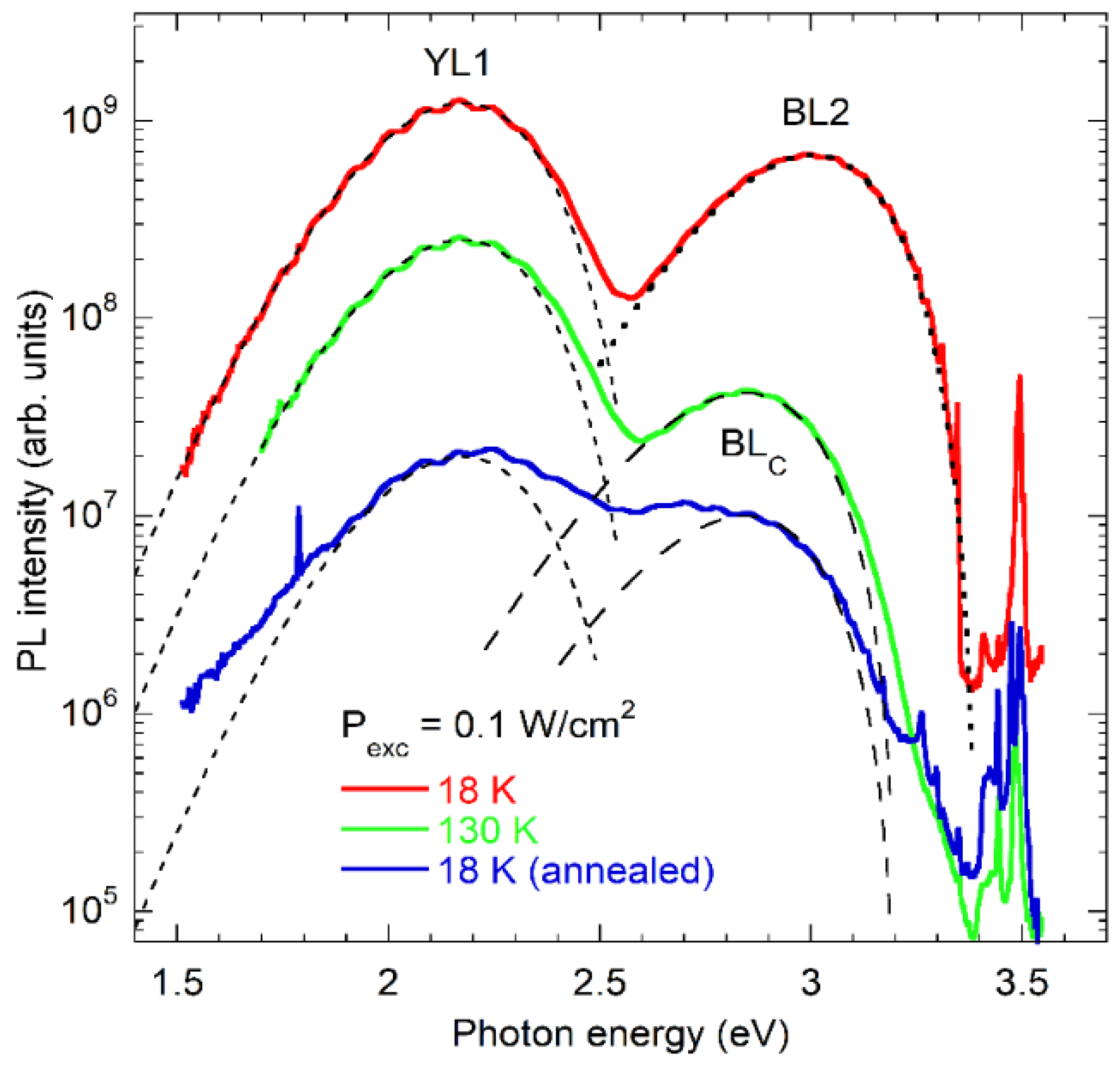
Figure 1 shows PL spectra measured at 18 and 130 K at relatively low excitation intensity (Pexc ≈ 0.1 W/cm2). In the as-grown sample, the YL1 and BL2 bands, attributed to the CN acceptor and CNHi donor, respectively, are very strong at T = 18 K [7,9]. To deconvolute the PL spectra, we simulated shapes of the broad PL bands with the following expression [18].
Here, Se is the Huang–Rhys factor, = E0 + 0.5 ħΩe, E0 is the ZPL energy, dgFC = − ħωmax is the Frank–Condon shift, ħΩe is the effective phonon mode energy, and ħω and ħωmax are the photon energy and PL band maximum, respectively. The Δ is a possible minor shift of the PL band maximum due to reasons, such as strain in GaN layers grown on foreign substrates. The shapes of PL bands are reproducible in different samples, and the parameters used in this work are the same as those published before [3].
With increasing temperature, the BL2 band is quenched above 100 K with the activation energy of 0.15 eV and completely disappears at 130 K. The BLC band with a maximum at 2.85 eV, well-resolved at 130 K, is attributed to transitions via the 0/+ level of the CN defect [9]. It is difficult to study the BLC band in as-grown GaN:C at low temperatures because of the much stronger BL2 band. However, after annealing in N2 ambient at 800 °C, the BL2 band disappears due to the removal of hydrogen from the sample [7], and the BLC band can be observed at 18 K (Figure 1).
The BLC band’s shape and fine structure can be better resolved at high excitation intensity when the YL1 band is saturated due to its much longer lifetime. In particular, the decay of the YL1 band in the studied samples is nonexponential at T = 18 K, and it persists for milliseconds, whereas the PL lifetime of the BLC band is about 1 ns [3]. Figure 2 shows the PL spectrum obtained with a focused laser beam (Pexc ≈ 100 W/cm2).
The inset to this figure depicts the high-energy part of the spectrum. Resonance Raman scattering lines (R4 and R5) are observed at 3.352 and 3.344 eV at distances from the HeCd laser line (3.8135 eV) multiple of the LO phonon energy in GaN (~92 meV). The donor-bound-exciton (DBE) line at 3.487 eV and the free exciton (FE) line at 3.494 eV have about the same intensity. Two LO phonon replicas of the FE line have a characteristic shape and support the assignment of the FE line [19]. The peak at 3.368 eV is likely an exciton bound to structural defects (the Y4 line at 3.35 eV in strain-free GaN) [2]. A weak peak at 3.277 eV is attributed to the donor–acceptor-pair component of the Mg-related UVL band [3]. A narrow line at 3.172 eV is the ZPL of the BLC band. The transformation of the PL spectrum with temperature (Figure 3) supports the above attributions.
From the positions of the BL2 band ZPL at 3.347 meV (before annealing), the DBE line at 3.487 eV, and the FE line at 3.494 eV (before and after annealing), we determine the strain-related blue shift as Δ = 17 meV and the bandgap Eg = 3.520 eV in the studied GaN:C. The ZPL of the BLC band is located at 3.172 eV (Figure 3). Assuming that all PL lines close to the bandgap are blue-shifted by 17 meV due to strain, we find that E0 = 3.155 eV in unstrained GaN. The ZPL does not shift with excitation intensity, as it is expected for an internal transition from an excited state of a deep donor to the ground state. With increasing temperature, the ZPL intensity decreases.
A shoulder at the high-energy side (indicated with the “+20 meV” arrow in Figure 3) emerges with increasing temperature from 30 to 80 K. The shoulder is attributed to transitions from the conduction band to the ground state of the CN+. Indeed, the ZPL of the BLC band, especially its high-energy side, broadens with increasing temperature much stronger than the excitonic lines or than is expected from thermal broadening. The transformation is similar to that for the CNHi donor responsible for the BL2 band [7]. By subtracting E0 + 0.02 eV from the bandgap, we obtain the 0/+ transition level of the CN defect at 0.33 ± 0.01 eV above the valence band in the limit of low temperatures. The ZPL at 3.17 eV and a peak at ~3.14 eV (labeled 1 in Figure 3) were observed in three GaN:C samples annealed at 800 °C.
4. Discussion
To study the phonon-related fine structure of the BLC band, we subtracted the smooth component described with Equation (1) with parameters for the BLC band shape. The obtained fine structure for two GaN:C samples is shown in Figure 4. A sharp line at 3.17 eV is identified as the ZPL of the BLC band. The FWHM of this line is about 3 meV when the monochromator slit is small enough. Replicas of the ZPL line at energies multiple of 91.2 meV are the crystal LO phonon replicas with phonon energy ħΩLO. A set of lines with ħΩ1 = 34.3 meV is attributed to a pseudo-local phonon mode.
Earlier [9], we explained the exponential decay of the BLC band after a laser pulse, with PL lifetime shorter than 1 ns in degenerate n-type GaN:C, Si samples and 2.5 ns in high-resistivity GaN:C samples, with the assumption that transitions from an excited state close to the conduction band to the ground 0/+ level and transitions from the conduction band to the same level have similar lifetimes and cannot be resolved. The evolution of the PL spectrum with temperature (Figure 3) agrees with the explanation of electron transitions given in Ref. [9] and indicates that the excited state is located at about 0.02 eV below the conduction band.
5. Conclusions
We studied carbon-doped GaN annealed at 800 °C. The CN-related BLC band in these samples revealed the zero-phonon line at 3.17 eV and the phonon-related fine structure caused by LO phonons and a pseudo-local phonon with the energy of 34 meV. The 0/+ transition level of the CN defect was found at 0.33 ± 0.01 eV above the valence band. The BLC band with a maximum at 2.85 eV was caused by electron transitions from an excited state at about 0.02 eV below the conduction band to the 0/+ level of the CN defect.
Funding
This research was funded by National Science Foundation, grant number DMR-1904861 and by the VCU PeRQ award.
Data Availability Statement
The data that support the findings of this study are available from the corresponding author upon reasonable request.
Acknowledgments
The author would like to thank Strittmatter (Institute für Physik, Magdeburg, Germany) for providing GaN:C samples and Ye (VCU, USA) for annealing these samples.
Conflicts of Interest
The author declares no conflict of interest.
Sample Availability
Samples of the compounds are available from the authors.
References
- Morkoç, H. Handbook of Nitride Semiconductors and Devices; Wiley: New York, NY, USA, 2008. [Google Scholar]
- Reshchikov, M.A.; Morkoç, H. Luminescence properties of defects in GaN. J. Appl. Phys. 2005, 97, 061301. [Google Scholar] [CrossRef]
- Reshchikov, M.A. Measurement and analysis of photoluminescence in GaN. J. Appl. Phys. 2021, 129, 121101. [Google Scholar] [CrossRef]
- Lyons, J.L.; Wickramaratne, D.; Van de Walle, C.G. A first-principles understanding of point defects and impurities in GaN. J. Appl. Phys. 2021, 129, 111101. [Google Scholar] [CrossRef]
- Demchenko, D.O.; Reshchikov, M.A. Blue luminescence and Zn acceptor in GaN. Phys. Rev. B 2013, 88, 115204. [Google Scholar] [CrossRef] [Green Version]
- Reshchikov, M.A.; McNamara, J.D.; Zhang, F.; Monavarian, M.; Usikov, A.; Helava, H.; Makarov, Y.; Morkoç, H. Zero-phonon line and fine structure of the yellow luminescence band in GaN. Phys. Rev. B 2016, 94, 035201. [Google Scholar] [CrossRef] [Green Version]
- Reshchikov, M.A.; Andrieiev, O.; Vorobiov, M.; McEwen, B.; Shahedipour-Sandvik, F.; Ye, D.; Demchenko, D.O. Stability of the CNHi complex and the BL2 luminescence band in GaN. Phys. Stat. Sol. 2021, 2100392. [Google Scholar] [CrossRef]
- Ogino, T.; Aoki, M. Mechanism of Yellow Luminescence in GaN. Jpn. J. Appl. Phys. 1980, 19, 2395–2405. [Google Scholar] [CrossRef]
- Reshchikov, M.A.; Vorobiov, M.; Demchenko, D.O.; Özgür, Ü.; Morkoç, H.; Lesnik, A.; Hoffmann, M.P.; Hörich, F.; Dadgar, A.; Strittmatter, A. Two charge states of the CN acceptor in GaN: Evidence from photoluminescence. Phys. Rev. B 2018, 98, 125207. [Google Scholar] [CrossRef] [Green Version]
- Lyons, J.L.; Janotti, A.; Van de Walle, C.G. Effects of carbon on the electrical and optical properties of InN, GaN, and AlN. Phys. Rev. B 2014, 89, 035204. [Google Scholar] [CrossRef]
- Matsubara, M.; Belotti, E. A first-principles study of carbon-related energy levels in GaN. I. Complexes formed by substitutional/interstitial carbons and gallium/nitrogen vacancies. J. Appl. Phys. 2017, 121, 195701. [Google Scholar] [CrossRef] [Green Version]
- Zhang, H.-S.; Shi, L.; Yang, X.-B.; Zhao, Y.-J.; Xu, K.; Wang, L.-W. First-principles calculations of quantum efficiency for point defects in semiconductors: The example of Yellow luminescence by GaN:CN + ON and GaN:CN. Adv. Opt. Mater. 2017, 5, 1700404. [Google Scholar] [CrossRef]
- Deak, P.; Lorke, M.; Aradi, B.; Frauenheim, T. Carbon in GaN: Calculations with an optimized hybrid functional. Phys. Rev. B 2019, 99, 085206. [Google Scholar] [CrossRef]
- Narita, T.; Tomita, K.; Tokuda, Y.; Kogiso, T.; Horita, M.; Kachi, T. The origin of carbon-related carrier compensation in p-type GaN grown by MOVPE. J. Appl. Phys. 2018, 124, 215701. [Google Scholar] [CrossRef]
- Reshchikov, M.A. Point defects in GaN. In Semiconductors and Semimetals: Defects in Semiconductors; Jagadish, C., Privitera, V., Romano, L., Eds.; Academic Press: Burlington, UK, 2015; Volume 91, pp. 315–367. ISBN 978-0-12-801935-1. [Google Scholar]
- Wickramaratne, D.; Dreyer, C.E.; Monserrat, B.; Shen, J.-X.; Lyons, J.L.; Alkauskas, A.; Van de Walle, C.G. Defect identification based on first-principles calculations for deep level transient spectroscopy. Appl. Phys. Lett. 2018, 113, 192106. [Google Scholar] [CrossRef] [Green Version]
- Lesnik, A.; Hoffmann, M.P.; Fariza, A.; Bläsing, J.; Witte, H.; Veit, P.; Hörich, F.; Berger, C.; Hennig, J.; Dadgar, A.; et al. Properties of C-doped GaN. Phys. Stat. Sol. 2016, 254, 1600708. [Google Scholar] [CrossRef]
- Reshchikov, M.A.; Demchenko, D.O.; McNamara, J.D.; Fernández-Garrido, S.; Calarco, R. Green luminescence in Mg-doped GaN. Phys. Rev. B 2014, 90, 035207. [Google Scholar] [CrossRef] [Green Version]
- Kovalev, D.; Averboukh, B.; Volm, D.; Meyer, B.K. Free exciton emission in GaN. Phys. Rev. B 1996, 54, 2518–2522. [Google Scholar] [CrossRef] [PubMed]
Figure 1.
PL spectra at 18 and 130 K for as-grown GaN:C and at 18 K after annealing at Tann = 800 °C. The BL2 band is completely quenched at 130 K, revealing the BLC band. In the annealed sample, the BL2 band is not found even at 18 K. The dashed lines are calculated using Equation (1) with the following parameters: Se = 7.7, = 2.67 eV and dgFC = 0.50 eV (YL1 band); Se = 4.4, = 3.38 eV and dgFC = 0.38 eV (BL2 band); and Se = 3.5, = 3.2 eV and dgFC = 0.35 eV (BLC band). Δ = 0.01 eV. A sharp line at 1.79 eV is caused by an internal transition in Cr3+ ions in the sapphire substrate, which becomes noticeable when the PL signal from GaN is weak.

Figure 2.
PL spectrum at 18 K and Pexc = 100 W/cm2 from GaN:C annealed at Tann = 800 °C. The dashed lines are calculated using Equation (1) with the same parameters as in Figure 1. The inset zooms in the high-energy part of the spectrum.
Figure 2.
PL spectrum at 18 K and Pexc = 100 W/cm2 from GaN:C annealed at Tann = 800 °C. The dashed lines are calculated using Equation (1) with the same parameters as in Figure 1. The inset zooms in the high-energy part of the spectrum.

Figure 3.
Transformation of PL spectrum with temperature (Pexc = 100 W/cm2). The ZPL of the BLC band at 3.172 eV decreases, and a shoulder indicated with the arrow “+20 meV” increases with temperature.
Figure 3.
Transformation of PL spectrum with temperature (Pexc = 100 W/cm2). The ZPL of the BLC band at 3.172 eV decreases, and a shoulder indicated with the arrow “+20 meV” increases with temperature.

Figure 4.
PL spectra from two GaN:C samples (MD56 and MD146) after subtracting the dependence calculated using Equation (1) with parameters in Figure 1 for the BLC band. Pexc = 100 W/cm2. Two LO phonon replicas of the ZPL line at distances integer of ħΩLO = 91.2 meV and several pseudo-local phonon replicas (labeled with n = 1, 2 and 3) with ħΩ1 = 34.3 meV are indicated.

Publisher’s Note: MDPI stays neutral with regard to jurisdictional claims in published maps and institutional affiliations. |
© 2022 by the author. Licensee MDPI, Basel, Switzerland. This article is an open access article distributed under the terms and conditions of the Creative Commons Attribution (CC BY) license (https://creativecommons.org/licenses/by/4.0/).
Share and Cite
MDPI and ACS Style
Reshchikov, M.A. Fine Structure of the Carbon-Related Blue Luminescence Band in GaN. Solids 2022, 3, 231-236. https://0-doi-org.brum.beds.ac.uk/10.3390/solids3020016
AMA Style
Reshchikov MA. Fine Structure of the Carbon-Related Blue Luminescence Band in GaN. Solids. 2022; 3(2):231-236. https://0-doi-org.brum.beds.ac.uk/10.3390/solids3020016
Chicago/Turabian StyleReshchikov, Michael A. 2022. "Fine Structure of the Carbon-Related Blue Luminescence Band in GaN" Solids 3, no. 2: 231-236. https://0-doi-org.brum.beds.ac.uk/10.3390/solids3020016