
A New Design of a CMOS Vertical Hall Sensor with a Low Offset
by
 , ,
, ,
Fei Lyu
1 ,
,
Shuo Huang
1,
Chaoran Wu
1,
Xingcheng Liang
1,
Pengzhan Zhang
1,2,
Yuxuan Wang
2,
Hongbing Pan
2 and
Yu Wang
3,* 1
School of Electronics and Information Engineering, Jinling Institute of Technology, Nanjing 211169, China
2
School of Electronic Science and Engineering, Nanjing University, Nanjing 210023, China
3
School of Electronics Engineering, Nanjing Xiaozhuang University, Nanjing 211171, China
*
Author to whom correspondence should be addressed.
Sensors 2022, 22(15), 5734; https://0-doi-org.brum.beds.ac.uk/10.3390/s22155734
Submission received: 30 June 2022
/
Revised: 26 July 2022
/
Accepted: 29 July 2022
/
Published: 31 July 2022
(This article belongs to the Special Issue Magnetic Sensor and Its Applications)
Abstract
:Vertical Hall sensors (VHSs), compatible with complementary metal oxide semiconductor (CMOS) technology, are used to detect magnetic fields in the plane of the sensor. In previous studies, their performance was limited by a large offset. This paper reports on a novel CMOS seven-contact VHS (7CVHS), which is formed by adding two additional contacts to a traditional five-contact VHS (5CVHS) to alleviate the offset. The offset voltage and offset magnetic field of the 7CVHS are reduced by 90.20% and 88.31% of those of the 5CVHS, respectively, with a 16.16% current-related sensitivity loss. Moreover, the size and positions of the contacts are optimized in standard GLOBALFOUNDRIES 0.18 μm BCDliteTM technology by scanning parameters using FEM simulations. The simulation data are analyzed in groups to study the influence of the size and contact positions on the current-related sensitivity, offset voltage, and offset magnetic field.
1. Introduction
Magnetic sensors have been widely used for applications in current sensing [1,2,3], biosensors [4], and consumer devices [5,6]. Hall effect sensors, which can be integrated into signal conditioning circuits using complementary metal oxide semiconductor (CMOS) technology, have the largest market share among all kinds of magnetic sensors [7]. Horizontal Hall sensors (HHSs), which are used to detect the magnetic field orthogonal to its surface, can meet the requirements of most application scenarios [8]. However, a three-dimensional (3D) Hall sensor is necessary in some applications, such as the measurement of a 3D magnetic field [9] and a space angle [10,11,12]. The most straightforward and promising way to implement 3D Hall sensors is to arrange multiple HHSs and vertical Hall sensors (VHSs) to detect magnetic fields orthogonal and parallel to the surface, respectively. VHSs with low sensitivity and especially large offsets are a weakness of the implementation of 3D Hall sensors [13,14,15].
After the development of the five-contact VHS (5CVHS) in [16], several variations have been proposed to improve the performance of VHSs, such as the four-contact VHS (4CVHS) [17,18], six-contact VHS (6CVHS) [19], and eight-contact circular vertical Hall devices (8CCVHD) [20]. The 5CVHS is a research hotspot to improve its performance [13,14,15], and variations have been proposed to reduce the offset by a large loss of sensitivity to accommodate low-voltage CMOS technology [21,22]. A symmetric four-folded and three-contact VHS (4F-3CVHS) has been proposed to reduce offset [23,24,25,26]. 4F-3CVHS, which has four active regions connected by additional wires, effectively improves VHS performance by increasing VHS complexity.
In this paper, we propose a new design for a seven-contact VHS (7CVHS) by adding two additional contacts in the body of a 5CVHS to reduce offset. The working principle of the 7CVHS and a contrastive analysis of the 5CVHS and 7CVHS are described in Section 2. The size and distances of contacts corresponding to the optimal performance of the 7CVHS are obtained by scanning parameters using FEM simulation, and the influence mechanism of the size and distances of contacts on the current-related sensitivity, offset voltage, and offset magnetic field are analyzed in detail in Section 3. Finally, Section 4 concludes this work.
2. From Five-Contact to Seven-Contact VHS
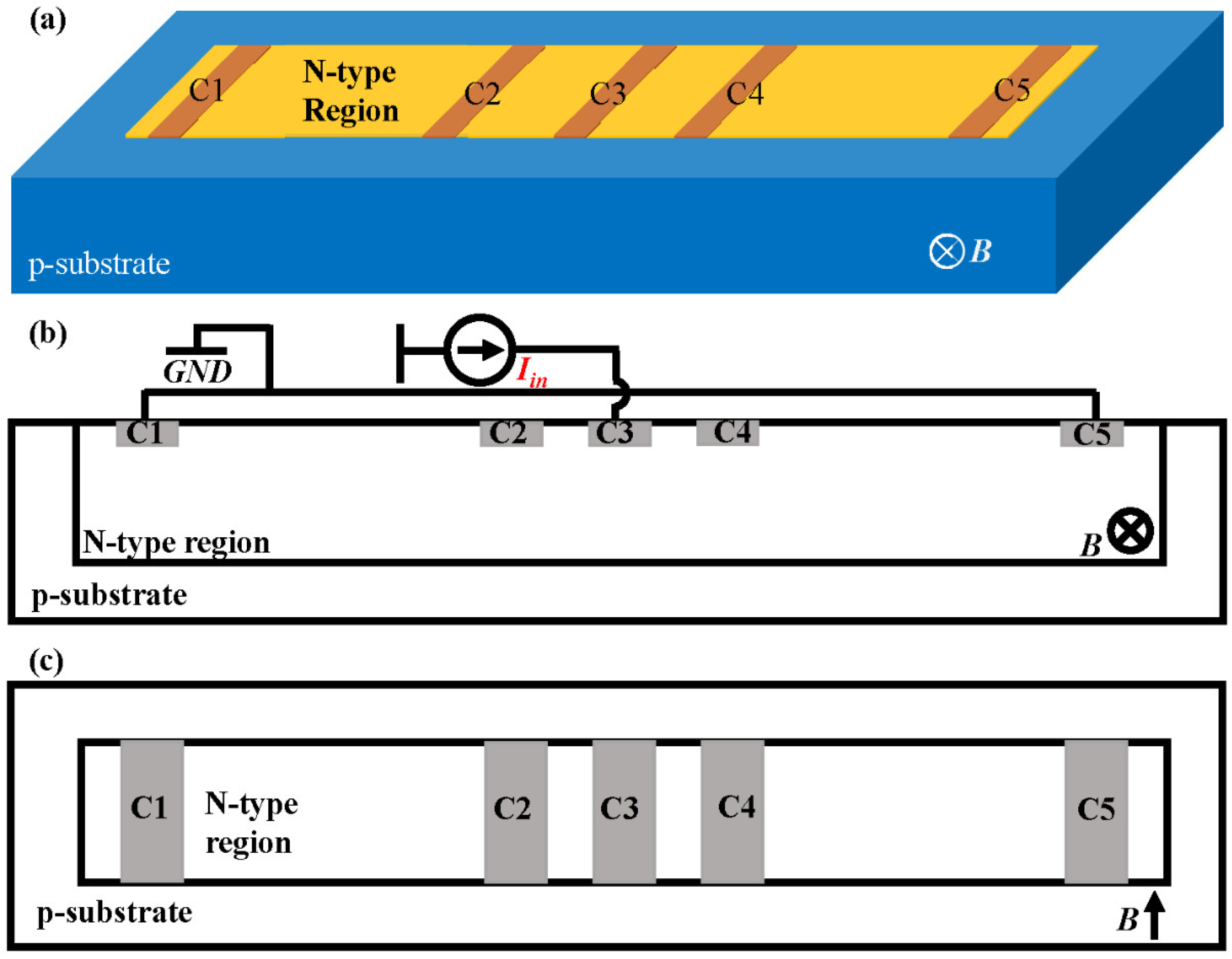
A 5CVHS, as shown in Figure 1, contains an N-type region in the p-substrate and five n+-diffusions serving as contacts from C1 to C5. The N-doped well, which works as an active region, largely determines the performance of 5CVHS. When the 5CVHS is working, the outer contacts, C1 and C5, are short-circuited, and a biasing current is applied between C3 and C1 (C5), as shown in Figure 1b. Obviously, the voltages of contacts C2 and C4 are equal because of the symmetry of the structure of 5CVHS. When the 5CVHS is placed in magnetic field B, the voltages of contacts C2 and C4 change because of the Hall effect. The Hall voltage is measured between C2 and C4. The Hall voltages of C2 and C4 have opposite directions, so the Hall voltage of the 5CVHS can be expressed as:
C2 and C4 serve as sensing contacts to obtain the Hall voltage of the 5CVHS. The voltage difference between them can be expressed as follows:
Combining Equations (1) and (2), we can obtain the expression
The main component of Vout is the Hall voltage, from which the magnetic field can be calculated by their relationship, as follows:
where SI is the current-related sensitivity of the 5CVHS, and Iin is the bias current applied between C3 and C1 (C5). The other part of Vout in Equation (3) is the voltage difference between C2 and C4 without a magnetic field, named the offset voltage Voff. The voltages of C2 and C4 should be equal in an ideal situation because of the symmetry structure of the 5CVHS on both sides of C3. However, offset voltage is unavoidable in engineering practice. The offset voltage can be converted to an offset magnetic field Boff, which is an important indicator of the sensor. Boff can be calculated using the following expression:
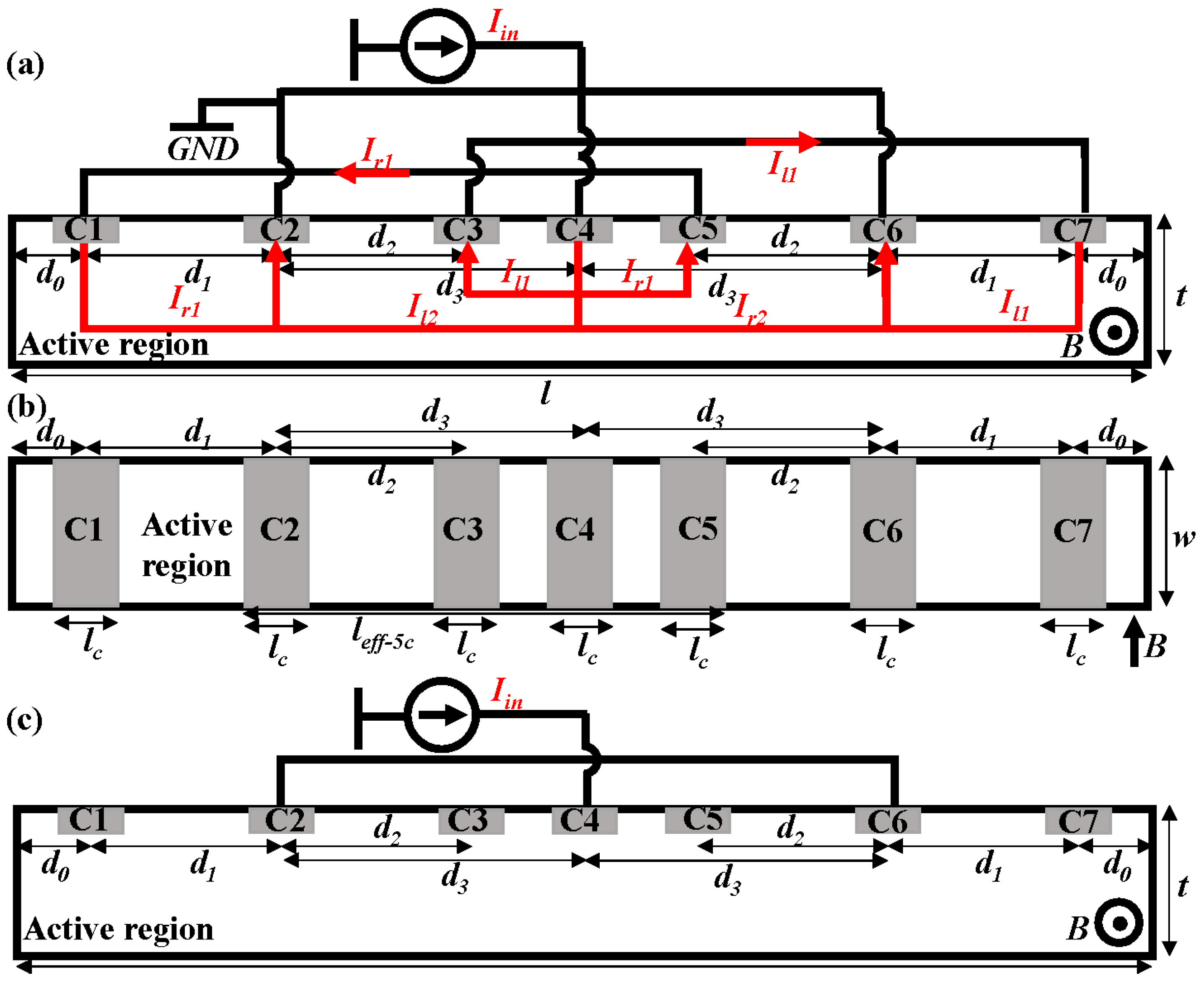
The offset is caused by asymmetry on both sides of C3 due to mask misalignment, the junction field effect (JFE), and piezoresistive effects. The new VHS, named the 7CVHS, shown in Figure 2a,b, introduces two connections on either side of C3 to neutralize the asymmetry and to lower the offset. The connections from C1 to C5 and C7 to C3, no doubt, lead to a decrease in the effective current of forming the Hall voltage. Thus, current-related sensitivity is reduced. The 7CVHS in the five-contact mode (7CVHS in 5C) in Figure 2c has the same characteristics as a 5CVHS. We compare a 7CVHS with the same size in the modes shown in Figure 2a,c to determine the advantage of the new VHS. Because the 7CVHS design is based on 5CVHS, it uses the same regions of technology. Additionally, 7CVHS is completely compatible with CMOS technology and contains an N-type region in the p-substrate and seven n+-diffusions serving as contacts from C1 to C7. The N-doped well works as an active region. An MVNVT is an N-type region, which is the most suitable area to implement the active region of the 7CVHS in standard GLOBALFOUNDRIES 0.18 μm BCDliteTM technology [27]. The doping concentration and depth of the MVNVT are 1.413 × 1017 cm−3 and 1.018 μm, respectively.
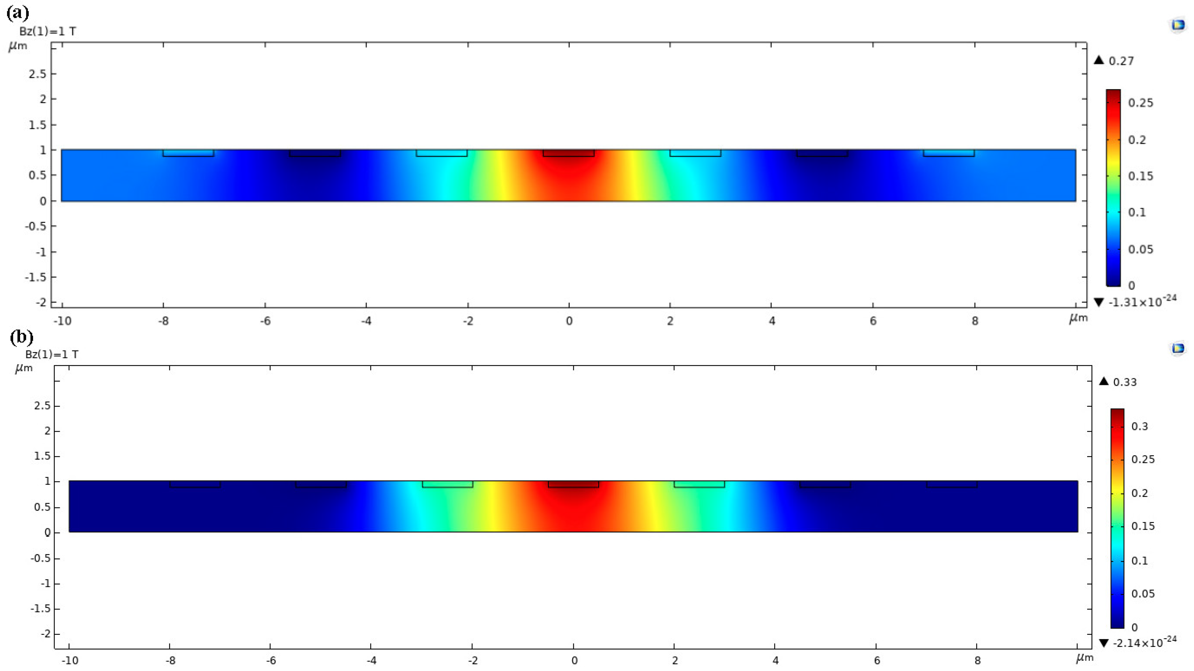
In the COMSOL model of 7CVHS, MVNVT is used as the active region. The models in COMSOL of two 7CVHS types and the voltage distributions on their surfaces are shown in Figure 3. The simulation setup parameters are given in Table 1. The size and performance comparisons of the model in Figure 2 are listed in Table 2. The offset magnetic field, expressed in Equation (5), is affected by the current-related sensitivity SI and the offset voltage Voff. The large current-related sensitivity, another important performance indicator of a VHS, is beneficial for suppressing the offset magnetic field. The biasing current and the magnetic field are set to 1 mA and 1 T, respectively, in the simulations to obtain current-related sensitivity. First, d1 changes to make C1 and C5 move away from C2 and C6 toward the left side of the 7CVHS when l, d2 and d3 remain the same to fix the positions of C2, C3, C4, C5, and C6. Second, d2 changes to make C3 move away from C2 toward C4 and C5 move away from C6 toward C4. The first step is repeated in one of d2. Third, d3 changes to make C2 and C6 move away from C4 toward both sides of the 7CVHS, and the second step is repeated on d3. Finally, l changes from 20 to 100 μm, and the third step is repeated on l. The offset is introduced by cutting C6 of 0.01 μm, and the size of the 7CVHS varies by l, d1, d2 and d3 operated by the above four steps to obtain the offset voltage in different sizes. We choose the structure of 7CVHS with the smallest value of Boff and list it in Table 2. As illustrated in Table 2, the offset voltage and offset magnetic field of the 7CVHS are reduced by 90.20% and 88.31% of those of the 5CVHS, respectively, with a 16.16% current-related sensitivity loss. We also compare the 7CVHS with the design in [21]. As illustrated in Table 3, the offset voltage and offset magnetic field of the 7CVHS are reduced by 99.77% and 99.56% of those of the 5CVHS, respectively, with a 43.09% current-related sensitivity loss.
3. 7CVHS Optimization
The current flows are illustrated in Figure 2a. The bias current Iin is divided into two currents to the left Il and to the right Ir when passing contact C4. Then, Il has two current branches, Il1 from C4 to C3 and Il2 from C4 to C2. Il2 is the effective current for forming the Hall voltage of C3. Il1 introduced by the connection between C3 and C4 is beneficial to the suppression of the offset voltage. However, Il1, which has the same result as the short-circuit effect, reduces the effective current of the Hall voltage in C3. Thus, the introduction of Il1 reduces the Hall voltage of C3. Il1 flows from C3 to C7 through an external connection. Then, Il1 flows from C7 to the left and into C6. The current Ir flowing to the right of C4 has the same characteristics. The Hall voltage measured between C1 (C5) and C7 (C3) is determined by the voltage variation caused by the Hall effect in contacts C1 to C7 and C3 to C5.
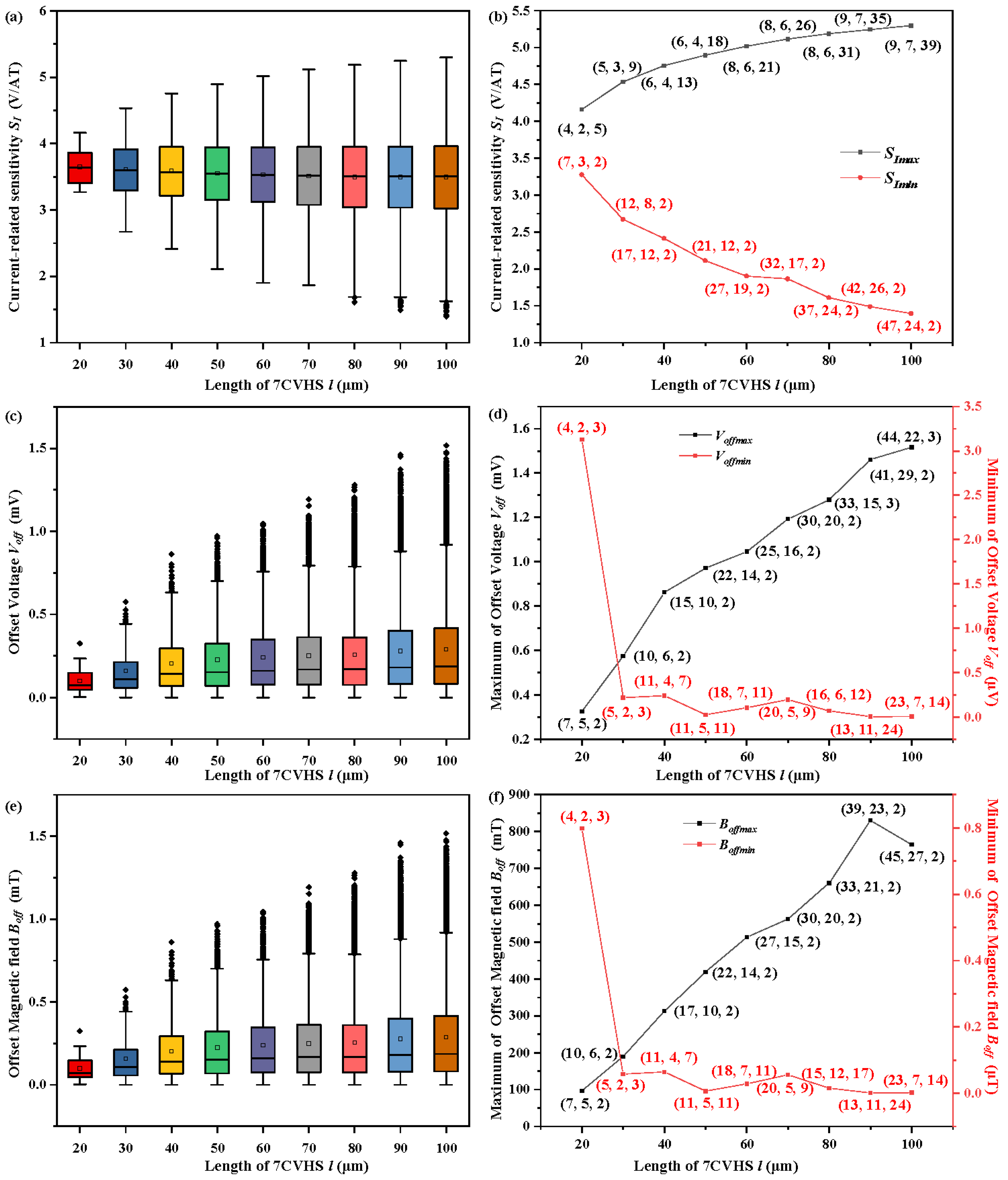
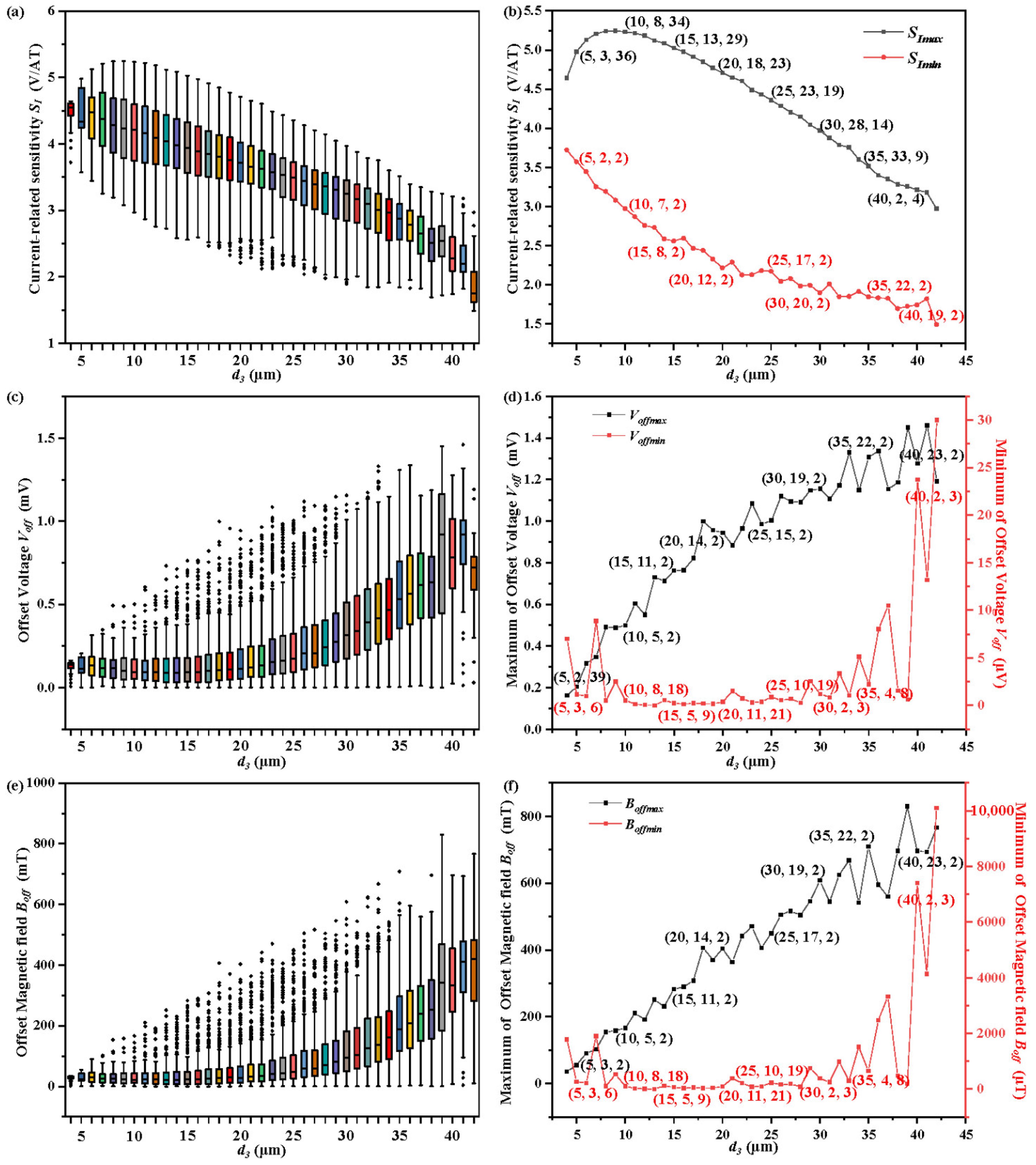
The current-related sensitivity SI of the 7CVHS of various lengths l are shown in Figure 4a. The maximum and minimum values of SI are extracted and shown in Figure 4b to clearly dictate the variation trend of SI. The other parameters d3, d2 and d1 corresponding to the maximum and minimum values of SI are marked by (d3, d2, d1) near the points in Figure 4b. The maximum value of SI increases due to its large length. The study and analysis in [27] confirm that the large length is beneficial to the increase in current-related sensitivity of the 5CVHS. The sensitivity of the 7CVHS, derived from the 5CVHS, is mainly determined by the Hall voltages of C3 and C5, which serve as sensing contacts in the 5CVHS. Thus, a large length contributes to the increase in the Hall voltages of C3 and C5. Although the large value of d3 makes the effective length of the 5CVHS in the 7CVHS containing C2, C3, C4, C5, and C6, the Hall voltages in C1 and C7 are weakened. However, the Hall voltage measured between C1 (C5) and C7 (C3) is determined by the voltage variation caused by the Hall effect in contacts C1 and C7, in addition to C3 and C5. Thus, the positions of C2 corresponding to the maximum values of SI are center-right between C4 and the left side of the 7CVHS to increase the Hall voltage in C1, and C7 and C5 are placed in the symmetrical position of C2 at the right side of C4. Moreover, the maximum values of SI correspond to the largest d2 to make C3 near C4. C3 has the largest Hall voltage when placed close to C4, as does C5. The last parameter d1 also should be the largest value to obtain the maximum values of SI. The large value of d1 makes C1 move away from C2 toward a lower Il1. However, the decrease in Il1 is beneficial to the increase in the Hall voltage in C5 and the measured Hall voltage. Moreover, Ir1 and Il1 obtain large growth spaces with large lengths. The minimum values of SI, as shown in Figure 4b with a red line, decrease with increasing length l of the 7CVHS. The values of d3 corresponding to the minimum values of SI are the largest to make C2 move away from C4. Meanwhile, there are few spaces to place C1, and d1 has no other alternative but is set as 2 μm. Thus, the Hall voltages in C1 and C7 are suppressed to make the measurement low. Moreover, the values of d2, which determine the locations of C3 and C5, have a large influence on the Hall voltage in C3 and C5. The large d2 making C3 move toward C4 is beneficial to the original Hall voltage of C3 but causes a large Ir1 and Il1 to lower the Hall voltage of C3. The values of d2 corresponding to the minimum values of SI make the C3 center-right balance the two above effects.
The offset voltages Voff of the 7CVHS of various lengths l are shown in Figure 4c. The maximum and minimum values of Voff are extracted and shown in Figure 4d to clearly reveal the variation trend of Voff. Almost all values of d1 corresponding to the maximum Voff are 2 μm to locate C1 near C2 and C7 near C6. The effective lengths of the 7CVHS from C1 to C7 are shortened in the above condition. A small effective length causes a large offset voltage [28]. The values of d2 and d3 are almost proportional to lowering the current Ir1 and Il1 and to enlarging the offset voltage Voff of the 7CVHS. The values of d1 corresponding to the minimum of Voff are large to make C1 move away from C2 and C7 move away from C6 and increase the effective length of the 7CVHS, but they are not the largest because Ir1 and Il1 decrease with increasing d1. Meanwhile, the values of d2 and d3 are set to make the current Ir1 and Il1 as large as possible.
The offset magnetic field Boff of the 7CVHS of various lengths l is shown in Figure 4e. The maximum and minimum values of Boff are extracted and shown in Figure 4f to clearly reveal the variation trend of Boff. Voff and Boff have almost the same relationship between the length of the 7CVHS l, and the values of d1, d2 and d3 corresponding to the maximum and minimum of Voff and Boff are almost the same. The offset voltage Voff has a large effect on the offset magnetic field Boff from the above comparison. The inflection point of the black line indicates that the current-related sensitivity SI of 7CVHS also affects the value of Boff. The smallest value of Boff is 0.8769 μT when the length of the 7CVHS is set to 90 μm.
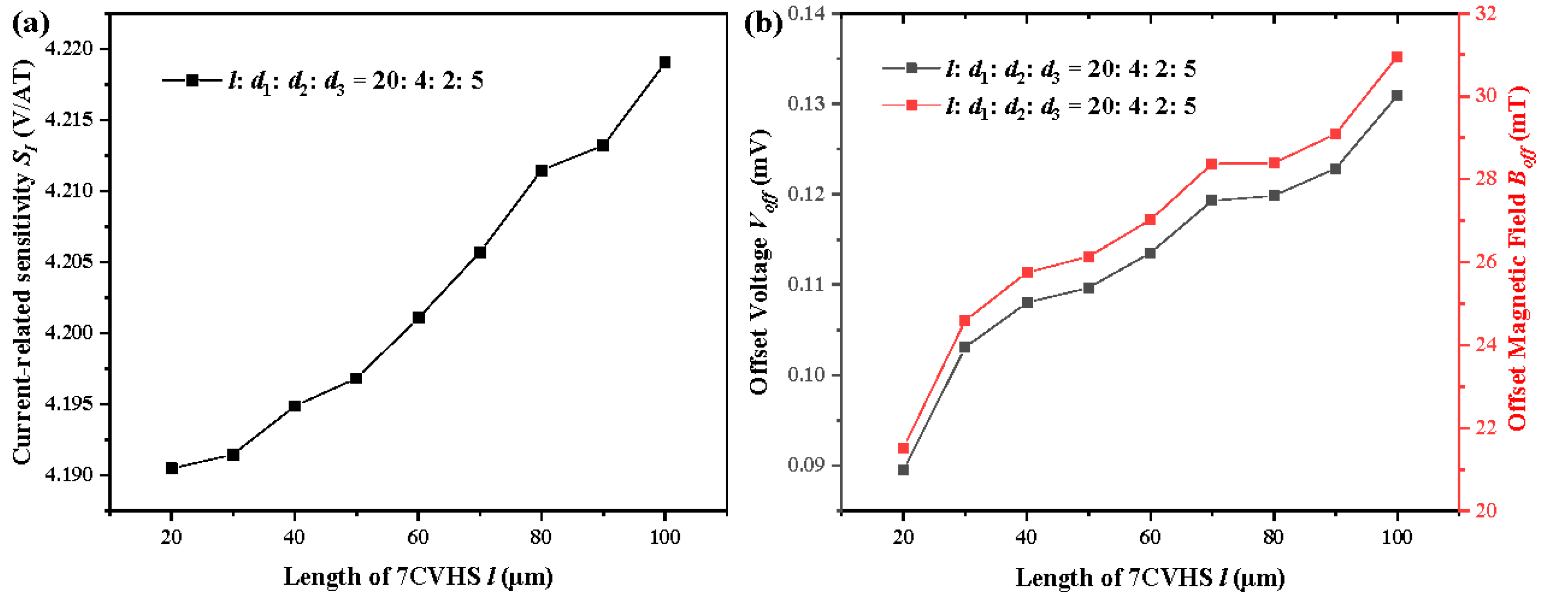
The variations in SI, Voff and Boff in Figure 4 depend not only on the variational values of l but also on the changes in d1, d2 and d3. To concentrate on the impacts of the length l on SI, Voff and Boff, the length l changes from 20 μm to 100 μm with the same ratio of values of l, d1, d2 and d3 as 20:4:2:5. The values of SI, Voff and Boff with l from 20 to 100 and the same ratio of values of l, d1, d2 and d3 are illustrated in Figure 5. As shown in Figure 5a, the values of SI increase with a large length. The same ratio of values of l, d1, d2 and d3 keeps the current allocation unchanged. That is, the currents Ir1, Ir2, Il1 and Il2 largely remain the same. However, the large length causes the proportions of the contacts to decrease. This reduces the short-circuit effect. As shown in Figure 5b, the values of Voff increase with a large length. A large length leads to a large resistance. In our design, a current source is used to bias the Hall sensor. Therefore, the supply voltage increases with a larger length, leading to a higher offset voltage. The gradient of SI is very small when compared with that of Voff. The impacts of the length on the offset magnetic field are basically in line with those on the offset voltage, as shown in Figure 5b.
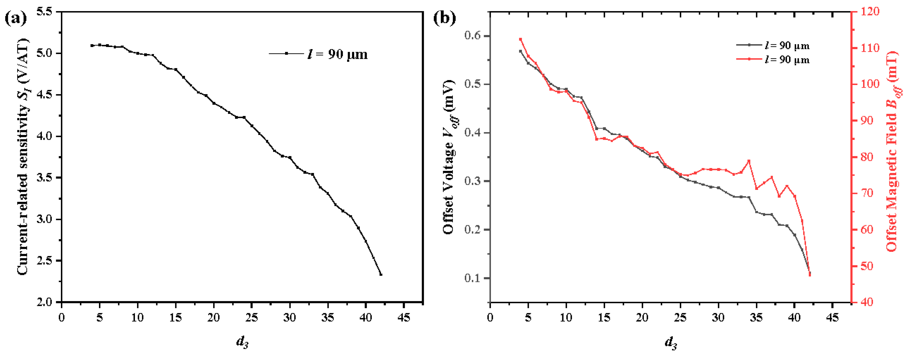
When the length l of the 7CVHS is set to 90 μm, the current-related sensitivities SI of various d3 from 4 to 42 μm in different d1 and d2 are obtained, as shown in Figure 6a. The maximum and minimum of the current-related sensitivity SImax and SImin of each d3 are extracted and shown in Figure 6b to study the relationship between SI and d3. The values of d1 of SImax are always large enough to lower the current Ir1 and Il1 to obtain the largest SI in a fixed d3. When d3 is small enough, leff-C5, the effective length of the 5CVHS in the 7CVHS, as shown in Figure 6b, is reduced, so the Hall voltages in contacts C3 and C5 are suppressed. SImax achieves short growth with an increase in d3 by enlarging leff-C5. However, SImax decreases as d3 continues to increase. Meanwhile, the increases in Ir1 and Il1 become the main factors that impact SImax and make SImax decrease with the increase in d3. Moreover, SImin is obtained with the smallest value of d1 to lower the currents Ir2 and Il2. The large d3 offers much space between C2 and C4 to place C3, and makes the current Ir2 and Il2 decrease. The large d3 causes a small SImax for this reason.
The offset voltage Voff of the same length 90 μm with various d3 from 4 to 42 μm in different d1 and d2 are obtained, as shown in Figure 6c. The maximum and minimum values of offset voltage Voffmax and Voffmin of each d3 are extracted, as shown in Figure 6b, to study the relationship between Voff and d3. The values of d1 are largely set as 2 μm to lower the currents Il1 and Ir1 and bring about the largest offset voltage Voffmax. Voffmax shows a rising trend overall with increasing d3 because a large d3 enlarges the bias voltage of the sensor. A large bias voltage increases the voltage of all parts of the sensor, including the offset voltages. Similar to the analysis in Figure 4c, almost all values of d1 corresponding to the maximum of Voff are 2 μm to move C1 near C2 and C7 near C6. The effective lengths of the 7CVHS from C1 to C7 are shortened in this condition to obtain a large offset voltage. The minimum values of the offset voltages appear with a large d1 to achieve a large effective length of 7CVHS.
The offset magnetic field Boff of the 7CVHS of various lengths d3 is shown in Figure 6e. The maximum and minimum values of Boff are extracted and shown in Figure 6f to clearly reveal the variation trend of Boff. Voff and Boff have almost the same relationship between d3, and the values of d1 and d2 corresponding to the maximum and minimum values of Voff and Boff are almost the same. The offset voltage Voff has a large effect on the offset magnetic field Boff from the above comparison. This point confirms the analysis and results shown in Figure 4.
To focus on the impacts of d3 on SI, Voff and Boff, we fix the distances of C3 to C4, C4 to C5, C1 to the left boundary, and C7 to the right boundary. In addition, the length of the 7CVHS is always set as 90 μm. Then, the value of d3 varies from 4 μm to 40.5 μm to simulate the values of SI, Voff and Boff. As shown in Figure 7a, the value of SI decreases with a large value of d3. With a large d3, the currents Ir2 and Il2 decrease because of the increase in their corresponding resistances. Thus, SI decreases because of the reduction in the effective current of the Hall voltage. Moreover, the currents Ir1 and Il1 increase because of the decrement of their corresponding resistances. Thus, the offset voltage decreases because of the large current needed to suppress the offset voltage, as shown in Figure 7b. The line of the offset magnetic field has a tendency similar to that of the offset voltage, as shown in Figure 7b. However, a small difference between them is derived from the variation in the value of SI.
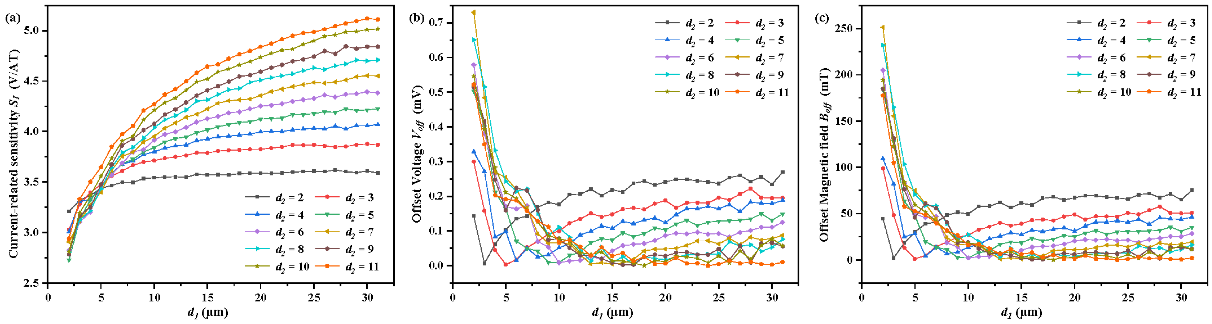
The relationship between the current-related sensitivity SI and d1 for various values of d2 is shown in Figure 8a. When d2 is unchanged, the growth of d1 is beneficial to the increase in SI by lowering the current Ir1 and Il1. When d1 is small enough, the small d2 also leads to a large SI by lowering the current Ir1 and Il1. When d1 becomes large, a large d2 brings about a large SI by making contacts C3 and C5 suitable to serve as sensing contacts with a large Hall voltage. The relationship between the offset voltage Voff with d1 for various values of d2 is shown in Figure 8b. When d2 is small, Voff decreases first with increasing d1 because a large d1 leads to low currents Il1 and Ir1. Then, the large d1 brings about the large effective length of the 7CVHS to make Voff. increase. When d2 is large, the increase in the effective length of the 7CVHS by enlarging the value of d1 always plays a leading role and determines the decrease in Voff. The relationship between the offset magnetic field Boff and d1 for various values of d2 is shown in Figure 8c. The values of d1 and d2 have the same effect on Voff and Boff, as seen by comparing Figure 8b,c. This point confirms the analysis and results shown in Figure 4 and Figure 6.
4. Conclusions
We have proposed a new design for a vertical Hall magnetic sensor with a low offset named 7CVHS. Two additional contacts are added to balance the asymmetry of the traditional 5CVHS. Comparing the 7CVHS with the 5CVHS shows that the offset voltage and the offset magnetic field are reduced by 90.20% and 88.31% of those of the 5CVHS, respectively, by a loss of 16.16% of the current-related sensitivity. Moreover, the length and distances of the contacts are optimized by scanning within the total coverage. When l, d3, d2, and d1 are set to 90, 13, 11, and 24 μm, respectively, the optimal performance of the 7CVHS is obtained, with the smallest offset magnetic field of 0.877 mT. In addition, the influence mechanisms of size and the distances of contacts on the current-related sensitivity, offset voltage, and offset magnetic field are studied by analyzing the data from different dimensions and perspectives.
Author Contributions
Data curation, S.H., C.W., X.L. and P.Z.; Formal analysis, Y.W. (Yuxuan Wang) and H.P.; Methodology, Y.W. (Yu Wang); Writing—original draft, F.L.; Writing—review & editing, F.L. and Y.W. (Yu Wang). All authors have read and agreed to the published version of the manuscript.
Funding
This work was supported by the Natural Science Foundation of the Jiangsu Higher Education Institutions of China under Grant 21KJB510012, the Scientific Research Foundation for the High-Level Talents of Jinling Institute of Technology under Grant jit-b-201907, the Scientific Research Incubation Foundation of Jinling Institute of Technology under Grant jit-fhxm-2007, and the Practice Innovation Training Program Projects for Jiangsu College Students under Grant 202213573086Y.
Conflicts of Interest
The authors declare no conflict of interest.
References
- Crescentini, M.; Marchesi, M.; Romani, A.; Tartagni, M.; Traverso, P.A. A Broadband, on-chip sensor based on hall effect for current measurements in smart power circuits. IEEE Trans. Instrum. Meas. 2018, 67, 1470–1485. [Google Scholar] [CrossRef]
- Weiss, R.; Itzke, A.; Reitenspieß, J.; Hoffmann, I.; Weigel, R. A novel closed loop current sensor based on a circular array of magnetic field sensors. IEEE Sens. J. 2019, 19, 2517–2524. [Google Scholar] [CrossRef]
- Mlejnek, P.; Ripka, P. Off-center error correction of AMR yokeless current transducer. J. Sens. 2017, 2017, 6057634. [Google Scholar] [CrossRef]
- Hall, D.A.; Gaster, R.S.; Makinwa, K.A.A.; Wang, S.X.; Murmann, B. A 256 Pixel magnetoresistive biosensor microarray in 0.18 µm CMOS. IEEE J. Solid-State Circuits 2013, 48, 1290–1301. [Google Scholar] [CrossRef] [PubMed]
- Ramsden, E. Hall-Effect Sensors: Theory and Application; Elsevier: Amsterdam, The Netherlands, 2011. [Google Scholar]
- Lenz, J.; Edelstein, S. Magnetic sensors and their applications. IEEE Sens. J. 2006, 6, 631–649. [Google Scholar] [CrossRef]
- Pan, H.; Yao, L.; He, S.; Li, W.; Li, L.; Sha, J. Single-chip integrated 3-d hall sensor. In Proceedings of the 2013 Third International Conference on Instrumentation, Measurement, Computer, Communication and Control, Shenyang, China, 21–23 September 2013; Volume 2013, pp. 252–255. [Google Scholar]
- Popovic, R.S. Hall Effect Devices; CRC Press: Boca Raton, FL, USA, 2003. [Google Scholar]
- Tomo, T.P.; Somlor, S.; Schmitz, A.; Jamone, L.; Huang, W.; Kristanto, H.; Sugano, S. Design and characterization of a three-axis hall effect-based soft skin sensor. Sensors 2016, 16, 491. [Google Scholar] [CrossRef]
- Schott, C.; Racz, R.; Huber, S. CMOS three axis Hall sensor and joystick application. In Proceedings of the Sensors, 2004 IEEE, Vienna, Austria, 24–27 October 2004; Volume 2, pp. 977–980. [Google Scholar]
- Jin, H.; Lu, H.; Cho, S.; Lee, J. Nonlinear compensation of a new noncontact joystick using the universal joint mechanism. IEEE/ASME Trans. Mechatron. 2007, 12, 549–556. [Google Scholar] [CrossRef]
- Jin, H.; Lu, H.; Cho, S.; Lee, J. Nonlinear compensation for non-contact electronic joystick with a single hall sensor. IET Sci. Meas. Technol. 2008, 2, 9–17. [Google Scholar] [CrossRef]
- Pascal, J.; Hébrard, L.; Frick, V.; Kammerer, J.-B.; Blondé, J.-P. Intrinsic limits of the sensitivity of CMOS integrated vertical Hall devices. Sens. Actuators A Phys. 2009, 152, 21–28. [Google Scholar] [CrossRef]
- Lyu, F.; Wang, Y. Current-related sensitivity optimization of CMOS five-contact vertical Hall sensor. J. Magn. Magn. Mater. 2020, 497, 166069. [Google Scholar] [CrossRef]
- Paul, O.; Raz, R.; Kaufmann, T. Analysis of the offset of semiconductor vertical Hall devices. Sens. Actuators A Phys. 2012, 174, 24–32. [Google Scholar] [CrossRef]
- Popovic, R.S. The vertical hall-effect device. IEEE Electron Device Lett. 1984, 5, 357–358. [Google Scholar] [CrossRef]
- Schott, C.; Besse, P.A.; Popovic, R.S. Planar hall effect in the vertical hall sensor. Sens. Actuators A Phys. 2000, 85, 111–115. [Google Scholar] [CrossRef]
- Falk, U. A symmetrical vertical hall-effect device. Sens. Actuators A Phys. 1990, 22, 751–753. [Google Scholar] [CrossRef]
- Schurig, E.; Schott, C.; Besse, P.A.; Demierre, M.; Popovic, R.S. 0.2 mT Residual offset of CMOS integrated vertical Hall sensors. Sens. Actuators A Phys. 2004, 110, 98–104. [Google Scholar] [CrossRef]
- Banjevic, M.; Furrer, B.; Blagojevic, M.; Popovic, R.S. High-speed CMOS magnetic angle sensor based on miniaturized circular vertical Hall devices. Sens. Actuators A Phys. 2012, 178, 64–75. [Google Scholar] [CrossRef]
- Pascal, J.; Hébrard, L.; Kammerer, J.-B.; Frick, V.; Blondé, J.-P. First vertical hall device in standard 0.35 μm cmos technology. Sens. Actuators A Phys. 2008, 147, 41–46. [Google Scholar] [CrossRef]
- Osberger, L.; Frick, V.; Hébrard, L. High resolution shallow vertical Hall sensor operated with four-phase bi-current spinning current. Sens. Actuators A Phys. 2016, 244, 270–276. [Google Scholar] [CrossRef]
- Sander, C.; Vecchi, M.-C.; Cornils, M.; Paul, O. From three-contact vertical hall elements to symmetrized vertical hall sensors with low offset. Sens. Actuators A Phys. 2016, 240, 92–102. [Google Scholar] [CrossRef]
- Sander, C.; Leube, C.; Paul, O. Compact two-dimensional CMOS Hall sensor based on switchable configurations of four three-contact elements. Sens. Actuators A Phys. 2016, 248, 281–289. [Google Scholar] [CrossRef]
- Sander, C.; Leube, C.; Paul, O. Novel compact two-dimensional cmos vertical hall sensor. In Proceedings of the 2015 Transducers-2015 18th International Conference on Solid-State Sensors, Actuators and Microsystems (TRANSDUCERS), Anchorage, AK, USA, 21–25 June 2015; pp. 1164–1167. [Google Scholar]
- Sander, C.; Raz, R.; Ruther, P.; Paul, O.; Kaufmann, T.; Cornils, M.; Vecchi, M.C. Fully symmetric vertical hall devices in CMOS technology. In Proceedings of the Sensors, 2013 IEEE, Baltimore, MD, USA, 3–6 November 2013; pp. 1–4. [Google Scholar]
- Lyu, F.; Zhang, Z.; Toh, E.-H.; Liu, X.; Ding, Y.; Pan, Y.; Li, C.; Li, L.; Sha, J.; Pan, H. Performance comparison of cross-like hall plates with different covering layers. Sensors 2014, 15, 672–686. [Google Scholar] [CrossRef] [PubMed] [Green Version]
- Lyu, F.; Zhang, Z.; Pan, Y.; Toh, E.H.; Liu, X.; Ding, Y.; Qing, Z.; He, S.; Li, L.; Pan, H. A mask-misalignment offset reduction method for design of cross-like cmos hall devices. In Proceedings of the 2016 Sixth International Conference on Instrumentation & Measurement, Computer, Communication and Control (IMCCC), Harbin, China, 21–23 July 2016; pp. 150–154. [Google Scholar]
Figure 1.
3D view (a), cross-section (b), and top view (c) of a 5CVHS implemented in CMOS technology.
Figure 1.
3D view (a), cross-section (b), and top view (c) of a 5CVHS implemented in CMOS technology.

Figure 2.
Cross-section (a) and top view (b) of the proposed 7CVHS. (c) 7CVHS in five-contact mode (5CVHS).
Figure 2.
Cross-section (a) and top view (b) of the proposed 7CVHS. (c) 7CVHS in five-contact mode (5CVHS).

Figure 3.
Models in COMSOL of 7CVHS (a) and 5CVHS (b), where the colors illustrate the voltage distributions.
Figure 3.
Models in COMSOL of 7CVHS (a) and 5CVHS (b), where the colors illustrate the voltage distributions.

Figure 4.
Current-related sensitivity SI (a), offset voltage Voff (c), and offset magnetic field Boff (e) of various lengths of the 7CVHS from 20 to 100 μm illustrated by boxplots. Maximum and minimum values of current-related sensitivity SImax and SImin (b), offset voltage Voffmax and Voffmin (d), and offset magnetic field Boffmax and Boffmin (f) in various lengths of the 7CVHS from 20 to 100 μm extracted from (a,c,d), respectively.

Figure 5.
Current-related sensitivity SI (a), offset voltage Voff and offset magnetic field Boff (b) of various lengths of the 7CVHS from 20 to 100 μm. The ratio of values of l, d1, d2 and d3 is always maintained at 20:4:2:5.
Figure 5.
Current-related sensitivity SI (a), offset voltage Voff and offset magnetic field Boff (b) of various lengths of the 7CVHS from 20 to 100 μm. The ratio of values of l, d1, d2 and d3 is always maintained at 20:4:2:5.

Figure 6.
Current-related sensitivity SI (a), offset voltage Voff (c), and offset magnetic field Boff (e) of d3 from 4 to 42 μm with the length l set to 90 μm illustrated by boxplots. Maximum and minimum values of current-related sensitivity SImax and SImin (b), offset voltage Voffmax and Voffmin (d), and offset magnetic field Boffmax and Boffmin (f) in d3 from 4 to 42 μm extracted from (a,c,d), respectively.

Figure 7.
Current-related sensitivity SI (a), offset voltage Voff and offset magnetic field Boff (b) of d3 from 4 to 42 μm with length l set to 90 μm. The distances of C3 to C4, C4 to C5, C1 to the left boundary, and C7 to the right boundary are fixed.
Figure 7.
Current-related sensitivity SI (a), offset voltage Voff and offset magnetic field Boff (b) of d3 from 4 to 42 μm with length l set to 90 μm. The distances of C3 to C4, C4 to C5, C1 to the left boundary, and C7 to the right boundary are fixed.

Figure 8.
Current-related sensitivity SI (a), offset voltage Voff (b), and offset magnetic field Boff (c) of d1 from 2 to 31 μm with the length l and d3 set to 90 μm and 24 μm, respectively.
Figure 8.
Current-related sensitivity SI (a), offset voltage Voff (b), and offset magnetic field Boff (c) of d1 from 2 to 31 μm with the length l and d3 set to 90 μm and 24 μm, respectively.


Table 1.
Simulation setup parameters.
| Symbol | Value | Description |
|---|---|---|
| q [C] | 1.602 × 10⁻¹⁹ | Electron charge |
| n [cm−3] | 1.413 × 10¹⁷ | Doping concentration |
| μ [cm2/Vsec] | 1000 | Electron mobility |
| B [T] | 1 | Magnetic field |
| t [m] | 1.018 × 10⁻⁶ | Depth of Hall sensor |
| w [m] | 3 × 10⁻⁶ | Width of Hall sensor |
| I [mA] | 1 | Bias current |
Table 2.
Size and performance comparison of the model in Figure 2.
Table 2.
Size and performance comparison of the model in Figure 2.
| Type of VHS | l (μm) | d1 (μm) | d2 (μm) | d3 (μm) | SI (V/AT) | Voff (mV) | Boff (mT) |
|---|---|---|---|---|---|---|---|
| 5CVHS | 90 | 13 | 11 | 24 | 5.94 | 4.45 × 10⁻² | 7.50 |
| 7CVHS | 4.98 | 4.36 × 10⁻³ | 0.877 | ||||
| −16.16% | −90.20% | −88.31% |
Table 3.
Performance comparison with the design in [21].
Publisher’s Note: MDPI stays neutral with regard to jurisdictional claims in published maps and institutional affiliations. |
© 2022 by the authors. Licensee MDPI, Basel, Switzerland. This article is an open access article distributed under the terms and conditions of the Creative Commons Attribution (CC BY) license (https://creativecommons.org/licenses/by/4.0/).
Share and Cite
MDPI and ACS Style
Lyu, F.; Huang, S.; Wu, C.; Liang, X.; Zhang, P.; Wang, Y.; Pan, H.; Wang, Y. A New Design of a CMOS Vertical Hall Sensor with a Low Offset. Sensors 2022, 22, 5734. https://0-doi-org.brum.beds.ac.uk/10.3390/s22155734
AMA Style
Lyu F, Huang S, Wu C, Liang X, Zhang P, Wang Y, Pan H, Wang Y. A New Design of a CMOS Vertical Hall Sensor with a Low Offset. Sensors. 2022; 22(15):5734. https://0-doi-org.brum.beds.ac.uk/10.3390/s22155734
Chicago/Turabian StyleLyu, Fei, Shuo Huang, Chaoran Wu, Xingcheng Liang, Pengzhan Zhang, Yuxuan Wang, Hongbing Pan, and Yu Wang. 2022. "A New Design of a CMOS Vertical Hall Sensor with a Low Offset" Sensors 22, no. 15: 5734. https://0-doi-org.brum.beds.ac.uk/10.3390/s22155734
Note that from the first issue of 2016, this journal uses article numbers instead of page numbers. See further details here.