1. Introduction
Three-level inverters are possible to generate five-level-step-shaped line to line voltage and three-level-step-shaped phase voltage. So the harmonics of the output voltage and current are reduced compared with conventional two-level inverters. Additionally, the emitter-collector voltage is only one half of that of conventional two-level inverters. Due to the low stress to switching devices, switching loss and switching noise are reduced [
1,
2,
3]. The topology of three-level inverters can be divided into three categories: cascade H-bridge (CHB) [
4], flying capacitor (FC) [
5], and neutral-point-clamped (NPC) [
6]. Among them, NPC three-level inverters are the most widely used in medium-voltage high-power industrial applications, such as traction drive, mine hoister, and wind power generation [
7,
8,
9].
The research of three-level inverter has been focused on output current ripple reduction [
10], neutral-point potential fluctuation restraint [
8,
11,
12], common mode voltage reduction [
13], switching loss suppression [
14], and low switching frequency operation [
15]. With these strategies, basic vectors used to synthesize the reference vector or dwell times of redundant switching states are changed to meet the requirement of a certain aspect of performance. When three-level inverters are applied in medium-voltage high-power motor drives, the output current ripple is increased because of the limitation of the switching frequency. Furthermore, with the increase of current harmonics and torque ripple, the additional loss and noise are introduced in both the inverter and the motor. As a result, how to evaluate and reduce the output current ripple of three-level inverters has been attracting attention from researchers all over the world.
In recent years, various evaluation methods, such as weighted total harmonic distortion (WTHD) [
15,
16], root-mean-square (RMS) value of stator flux ripple, [
17], and magnitude of the average current ripple vector [
10,
18], are proposed to evaluate the output ripple of the three-level inverter. If WTHD is regarded as the evaluation indicator of the output current ripple, the expression of each harmonic needs to be obtain by using a double-fourier transform of the output voltage. Unfortunately, the computational process is very complicated. And in most cases, it is convenient to compare PWM strategies based on the overall quality of output waveform rather than the individual harmonic produced by them. Thus, the RMS value of stator flux ripple and the magnitude of the average current ripple vector could be adopted to evaluate the output current ripple. Compared with WTHD, the computational burdens are lower.
Based on the above evaluation methods, lots of modulation strategies are presented to reduce the output current ripple of three-level inverters [
10,
16,
18], which can be divided into CPWM strategies and DPWM strategies. In reference [
18], the magnitude of the average current ripple vector is used as the indicator, and the dwell times of the two redundant switching states in continuous switching sequences are redistributed to reduce the output current ripple. DPWM methods for three-level inverters are proposed in reference [
16], and WTHD of the output voltage for both the CPWM and DPWM strategies are compared with each other. The concept of stator flux ripple is proposed in reference [
17], and the closed-form expressions of stator flux ripple for different switching sequences are obtained, and then the output performance of different switching sequences are compared with each other.
According to the above modulation strategies, it can be concluded that the current ripple of CPWM strategies is lower than that of DPWM strategies under a lower modulation index condition, while the conclusion is reversed under a higher modulation index condition. Thus, CPWM and DPWM strategies are both adopted in this paper. The closed-form expressions of the average current ripple vector for both the continuous and discontinuous switching sequences are derived. The sub-regions of different switching sequences are determined on the basis of the minimum value of magnitude of the average current ripple vector. Then a sector subdivision based SVPWM strategy with a reduced current ripple can be obtained.
2. Analysis of Switching Sequence in Space Vector Modulation Strategies
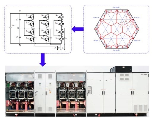
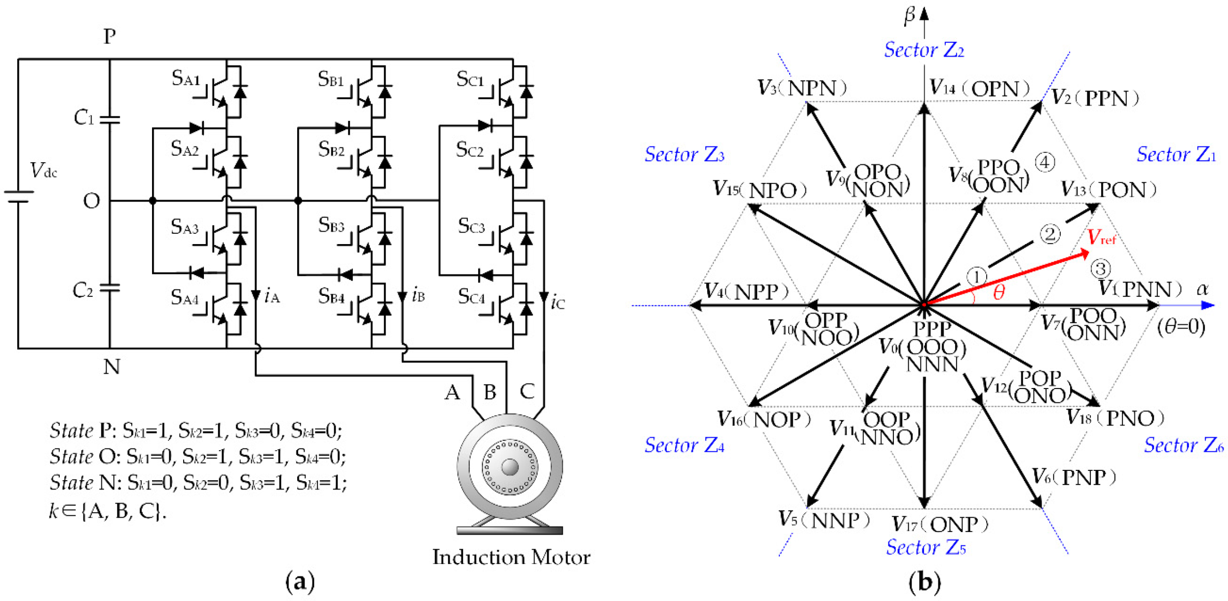
The topology of the NPC three-level inverter is shown in
Figure 1a. Each of three phases (A, B, and C) has three switching states (P, O, and N), so there are 3
3 = 27 switching state combinations for the three-level inverter. According to Park transformation in Equation (1), each combination can be represented by a basic space voltage vector
Vj,
j = 0, 1, 2, …, 18, as shown in
Figure 1b.
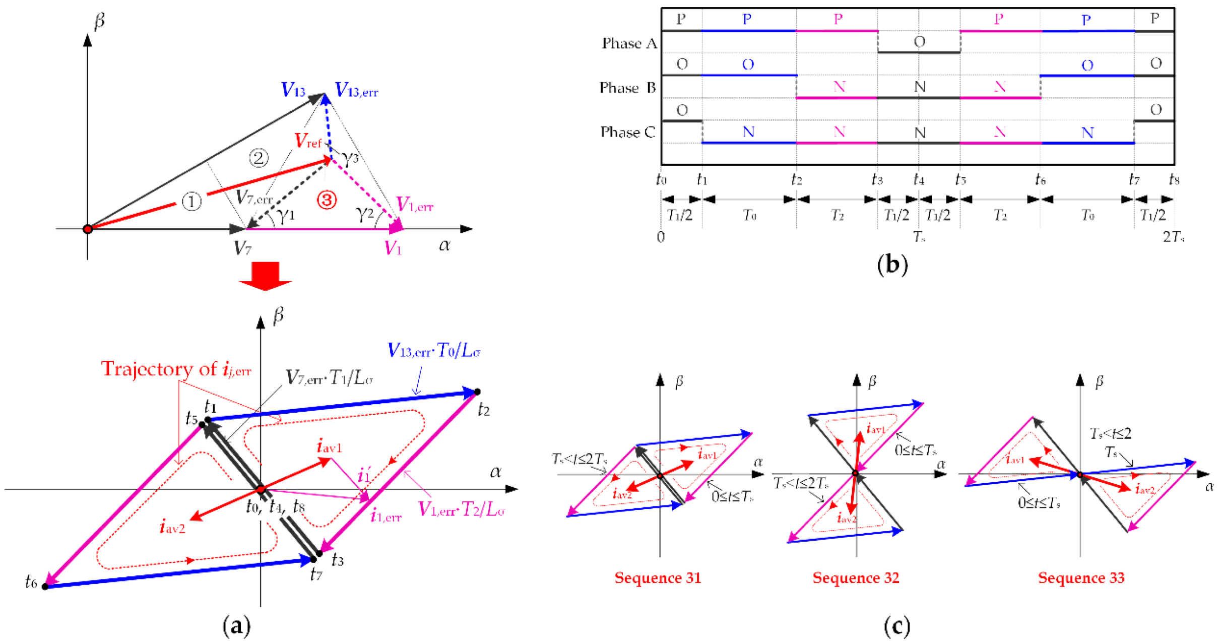
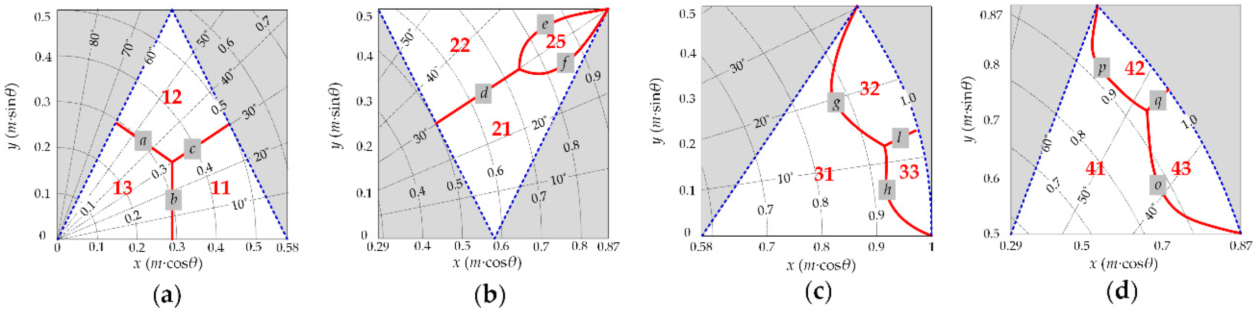
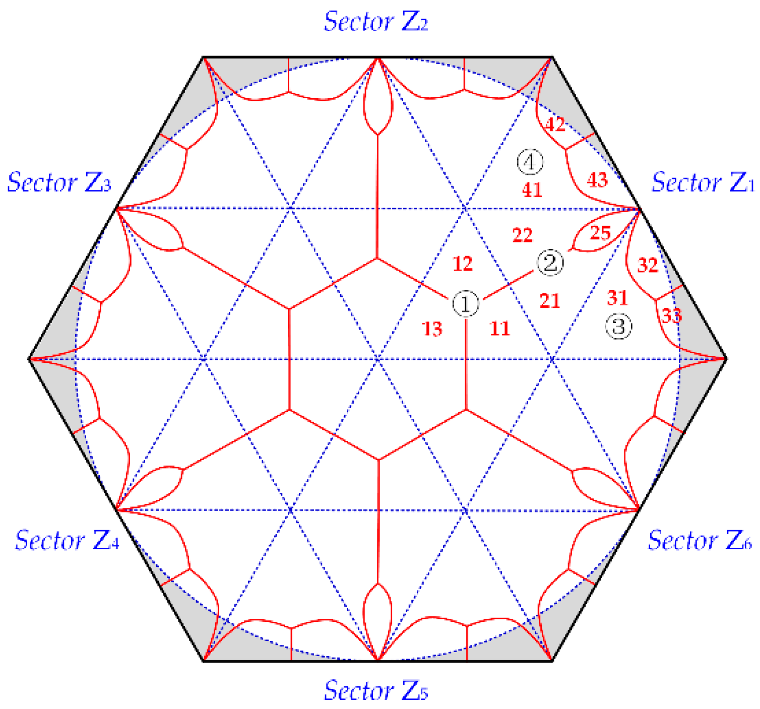
Based on the vector’s magnitude, 19 basic vectors can be divided into four categories, which are zero-voltage, small-voltage, medium-voltage and large-voltage. Zero vector V0 corresponds to three combinations, and each of small vectors V7 ~ V12 corresponds to two combinations. Different switching state combinations corresponding to the same voltage vector are defied as redundant switching states in this paper. The space vector hexagon could be symmetrically divided into six sectors Z1 ~ Z6, and every sector could be further divided into four triangles ① to ④.
The nearest three vectors are usually adopted to synthesize the reference voltage vector
Vref in three-level space vector PWM strategies. The dwell time of each vector can be solved by the principle of voltage-second balance. For example, when
Vref locates in triangle ③ of sector Z
1, yields
where
T1,
T2, and
T0 represent the dwell times of basic vector
V7,
V1, and
V13 in each sample period
Ts, respectively. The reference voltage vector
Vref can be synthesized by using various switching sequences. That is because each switching state can be arranged at any arbitrary time interval of each sample period and there are redundant switching states for basic voltage vectors
V0 and
V7 ~
V12.
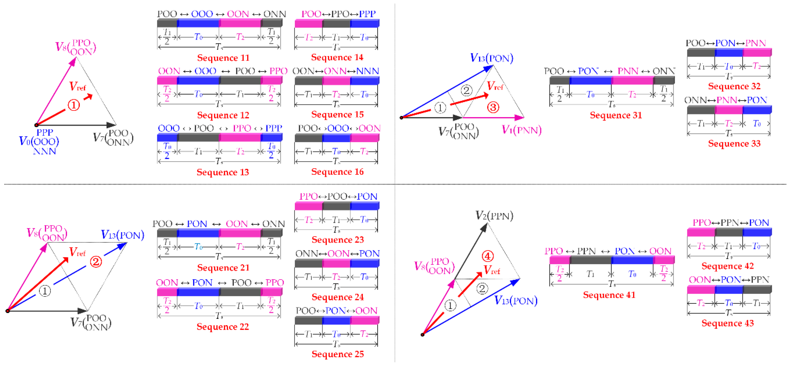
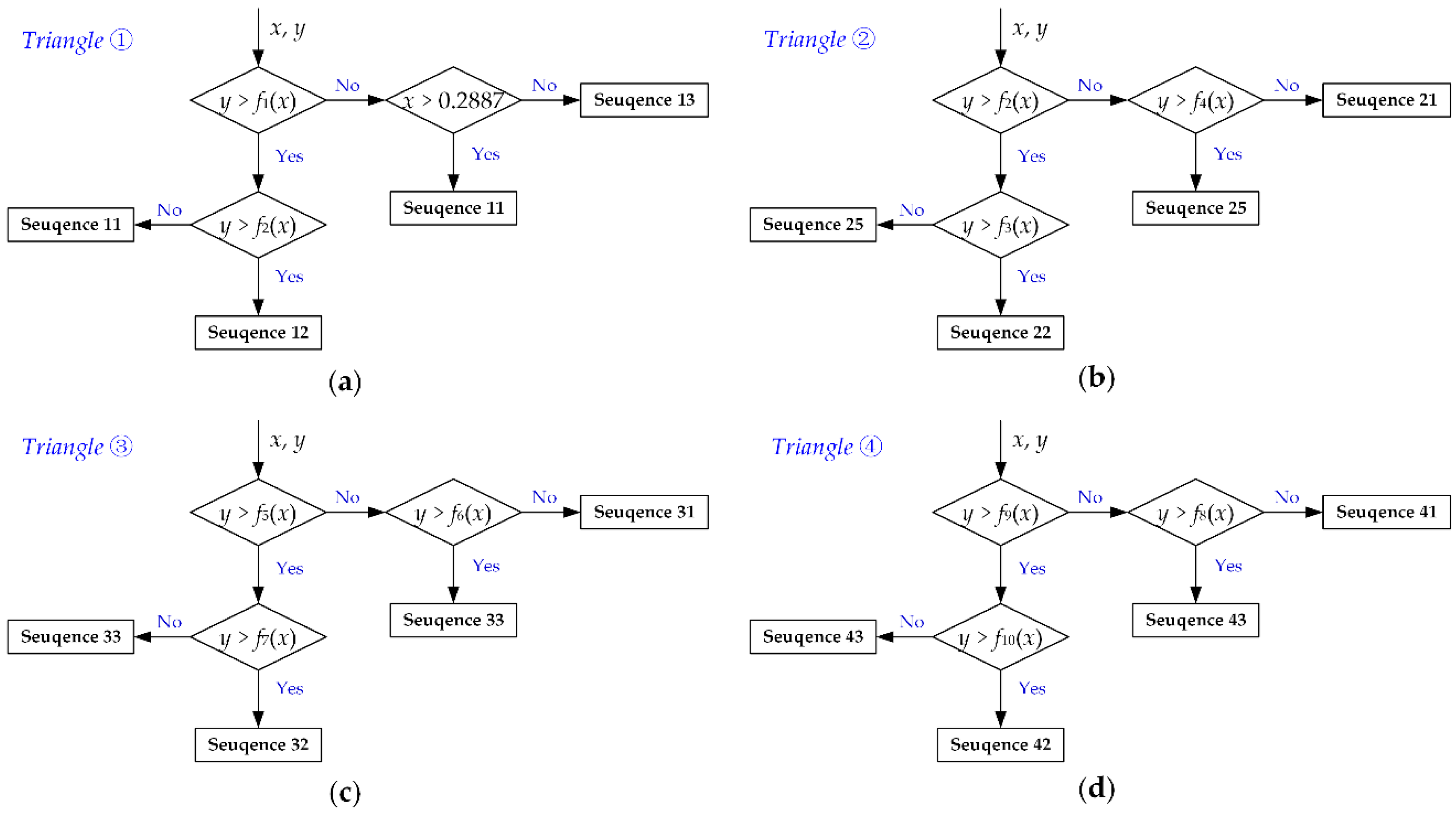
All the possible switching sequences synthesized the reference voltage vector
Vref in triangle ①–④ of sector Z
1 are shown in
Figure 2. The conditions that keep the switching loss as low as possible are listed as follows [
17]:
Based on the number of switching in each sample period, the switching sequences can be categorized into continuous switching sequences (Sequence 11, 12, 13, 21, 22, 31, and 41) and discontinuous switching sequences (Sequence 14, 15, 16, 23, 24, 25, 32, 33, 42, and 43). For discontinuous switching sequences, the switching only appears in two phase legs. Meanwhile for continuous switching sequences, the switching appears in all the three phase legs.
The switching sequences of space vector PWM strategies must be arranged symmetrically on both sides so that the switching sequence in a certain sample period is reversed in the next sample period. For example, if the switching sequence in one sample period is POO→PON→PNN→ONN, the sequence in the next sample period will be ONN→PNN→PON→POO, as shown in
Figure 3b.
Different arrangements of the switching sequence will inherently offer different behavior with regard to the performance indicators that can be used to assess the quality of the output waveform. Output current ripple of three-level inverters is used as the evaluation indicator and is analyzed in the next section.
3. Analysis of the Output Current Ripple
At any arbitrary instant in each sample period, there is always an error between the applied voltage and the reference voltage vector according to the principle of space vector PWM. The vector difference between
Vj and
Vref is defined as the voltage ripple vector
Vj,err. As shown in
Figure 3a, when
Vref is located in triangle ③ of sector Z
1, voltage ripple vectors corresponding to
V7,
V1, and
V13 are
V7,err,
V1,err, and
V13,err, respectively.
When the motor is driven by the voltage source inverter and the stator and rotor resistances are neglected, the voltage ripple vector
Vj,err will generate the current ripple vector
ij,err in the motor. The relationship of voltage and current ripple vectors in each
Ts can be indicated as follows
where
Lσ is the equivalent inductance of the motor. Take Sequence 31 as an example, as shown in
Figure 3a, when
t ∈ [0,
T1/2], the switching state POO is applied, the start point of
i7,err is at
t0. The direction of current ripple vector
ij,err lag the direction of voltage ripple vector
Vj,err by π/2 so that the end point of
i7,err travels from
t0 to
t1. When
t =
T1/2, |
i7,err| equals to |
V7,err·
T1/2
Lσ|. Similarly, the amplitude of current ripple vector are |
V13,err·
T0/
Lσ|, |
V1,err·
T2/
Lσ|, and |
V7,err·
T1/2
Lσ| when the switching state PON, PNN, and ONN are applied alternatively. The instants
t0~
t8 shown in
Figure 3a are corresponding to the instants shown in
Figure 3b. The trajectory of
ij,err during (0,
Ts] is triangle
t1–
t2–
t3–
t1. And the trajectory during (
Ts, 2
Ts] is triangle
t5–
t6–
t7–
t5. The lengths of three sides are
V7,err·
T1/
Lσ,
V1,err·
T2/
Lσ, and
V13,err·
T0/
Lσ, respectively.
The average current ripple vector in sample period (0,
Ts] and (
Ts, 2
Ts] are defined as follows
As shown in
Figure 3c, the shapes of triangle
t1–
t2–
t3–
t1 and
t5–
t6–
t7–
t5 are the same and are symmetrical about the origin. So
iav1 and
iav2 are equal in magnitude but opposite in direction. The conclusions derived in reference [
18] are as follows:
Conclusion 1. The terminal of the average current ripple vector is the mass center of the current ripple triangle.
In
Figure 3b, point G and G′ are the mass center of triangle
t1–
t2–
t3–
t1 and
t5–
t6–
t7–
t5, respectively. So the terminals of
iav1 and
iav2 are point G and G′. The square RMS value of the output current ripple is normally introduced to estimate the performance of the inverter, which is defined as follows
In sample period (0,
Ts], the current ripple vector can be divided into two parts
where auxiliary vector is the vector error between the current ripple vector
ij,err and the average current ripple vector
iav1. In time interval (0,
Ts], averaging Equation (6), yields
Substituting Equations (6) and (7) into Equation (5), yields
The trajectories of current ripple vector during (0, 2
Ts] corresponding to Sequence 31, 32, and 33 are shown in
Figure 3c. As can be seen, for different switching sequences, the relative positions of the mass center and the origin are different from each other, which means magnitudes of the average current ripple vectors are different. While shapes of current ripple triangles are the same. So the second item in the right side of Equation (8) is not changed. Then the following conclusion can be drawn:
Conclusion 2. The value of Irip_rms is determined by the value of |iav1|2. So the lower the value of |iav1|2 is, the better the output performance is.
4. The Expression of the Magnitude of the Average Current Ripple Vector
According to Conclusion 1 and Conclusion 2, the comparison of output performance for all the possible switching sequences can be replaced by the comparison of the distance between the mass center of current ripple triangle and the origin.
The modulation index
m is defined as
where
Vref is the amplitude of reference voltage vector,
Vdc is the amplitude of dc-link voltage. As shown in
Figure 3, the magnitudes of voltage ripple vector
V7,err,
V1,err, and
V13,err can be derived as follows
where
θ is the reference vector angle. According to Equation (2), the dwell time
T1,
T2, and
T0 corresponding to
V7,
V1, and
V13 during each sample period can be derived as follows
Based on Equations (10) and (11), and the geometric relationship in
Figure 3c, the closed-form expression of |
iav1| are listed in
Table 1.
Similarly, the expressions of other switching sequences in
Figure 2 also can be derived out. According to Equations (10) and (11), and
Table 1, it can be concluded that expressions of the magnitude of the average current ripple vector are functions of variable
Vdc,
Ts,
Lσ,
m and
θ. By developing expressions in
Table 1, it can be deduced that
VdcTs/
Lσ is the common item so that expressions can be considered as a function of
m and
θ (The detailed derivation process of |
iav1| is presented in
Appendix A).
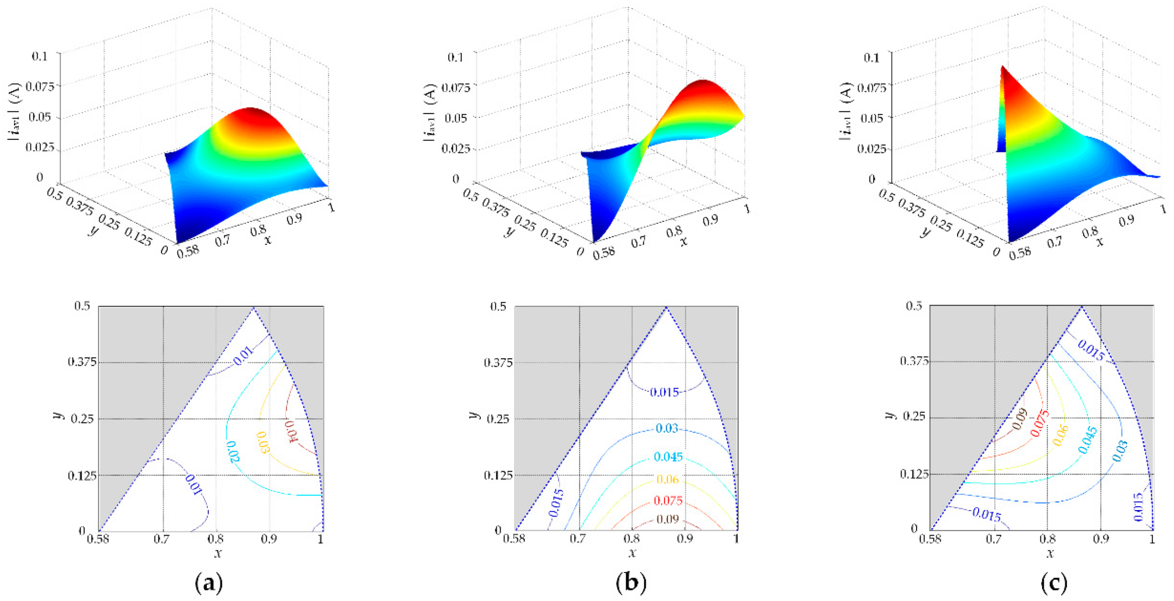
Let
x and
y to be
m·cos
θ and
m·sin
θ, respectively. The magnitude of the average current ripple vector |
iav1| of sector Z
1 in
x-
y rectangle coordinate system and the contour lines of |
iav1| in
x-
y plane corresponding to Sequence 31–33 are shown in
Figure 4. From
Figure 4, variation trends of |
iav1| corresponding to different sequences are not the same. If the switching sequence with the lowest |
iav1| is adopted at any arbitrary position, the output current ripple of the inverter will be minimized.
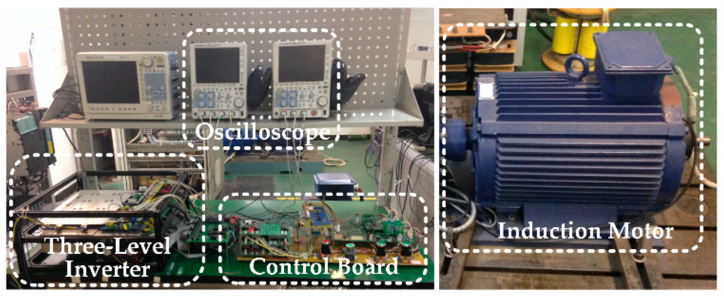
6. Experimental Verification
The proposed strategy, CPWM [
19] and DPWM3 (with the lowest distortion among DPWM0–DPWM3) [
20] are tested on the experimental prototype of three-level inverter fed induction motor shown in
Figure 8. Parameters of the experimental prototype are listed in
Table 2. The induction motor is driven with a constant
V/
f control.
6.1. The Proposed Sector Subdivision Based SVPWM Strategy
Instead of total harmonic distortion (THD), total demand distortion (TDD) is usually used as the output performance indicator of the inverter in a wide range of modulation index
m [
21], which is defined as follows
where
Ih is the
hth component of the output current and
IN is the rated current.
Ih and
IN are both RMS values.
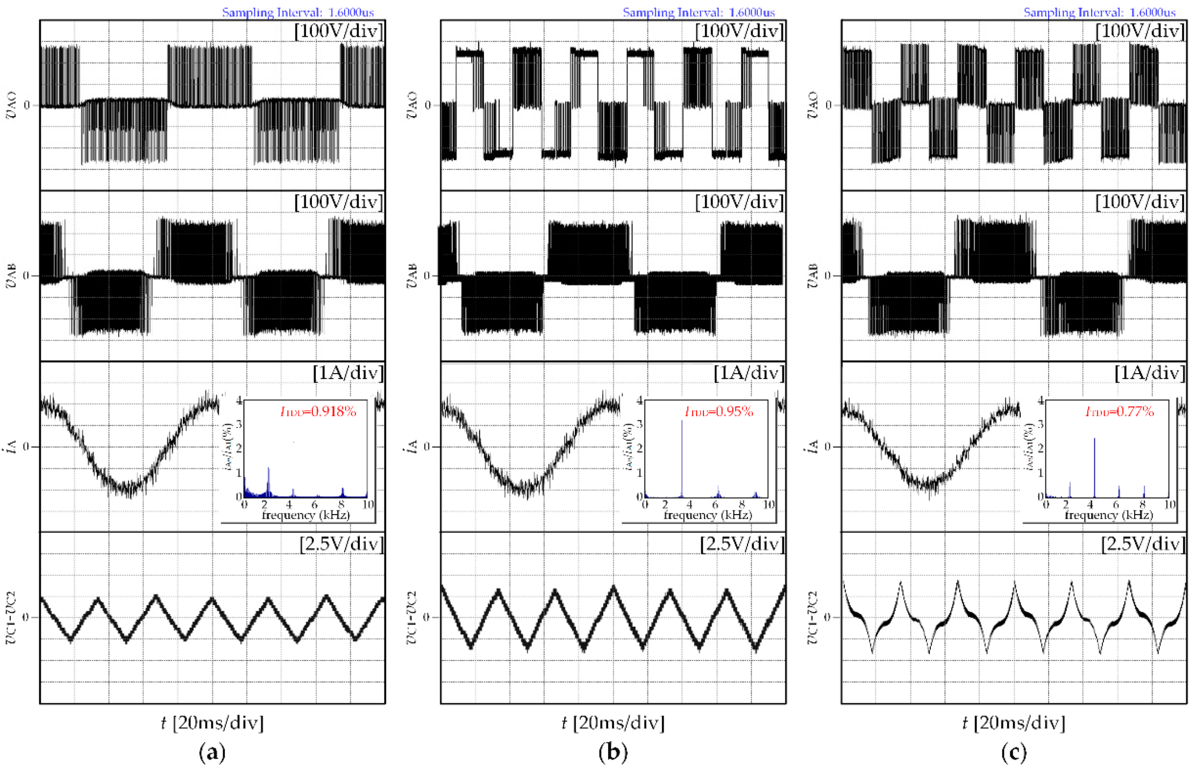
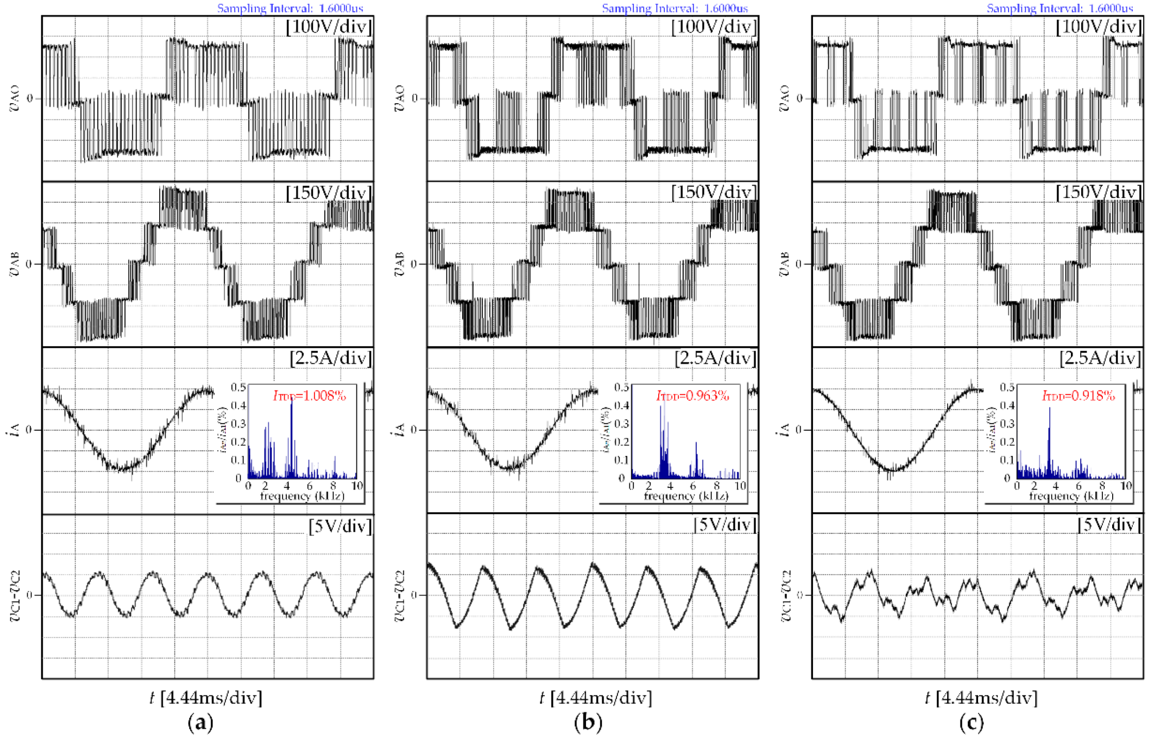
Experimental waveforms of output voltage
vAO and
vAB, output current
iA for CPWM, DPWM3, and the proposed strategy under conditions of
m = 0.2 and
m = 0.9 are presented in
Figure 9 and
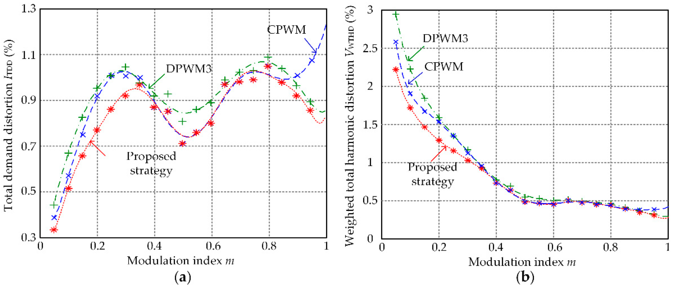
Figure 10, respectively. From
Figure 9 and
Figure 10,
ITDD of the proposed strategy is lower than that of CPWM and DPWM3.
According to experimental results, the fast fourier transformation (FFT) analysis tool in Matlab is used to calculate the
ITDD and
VWTHD under different modulation index conditions. Then variations of
ITDD and
VWTHD with the change of modulation index
m for CPWM, DPWM3, and the proposed strategy can be obtained, which is illustrated in
Figure 11a,b.
The weighted total harmonic distortion of output voltage
VWTHD is defined as
where
V1 and
Vh are the rms value of fundamental and
hth component of output voltage.
As shown in
Figure 11a, for the modulation index
m < 0.38 and
m ≥ 0.8,
ITDD of the proposed strategy is lower than that of CPWM and DPWM3. For the modulation index 0.38 ≤
m < 0.8, output waveform quality of the proposed strategy and CPWM are the same, which is still better than that of DPWM3. The same conclusion can be obtained from
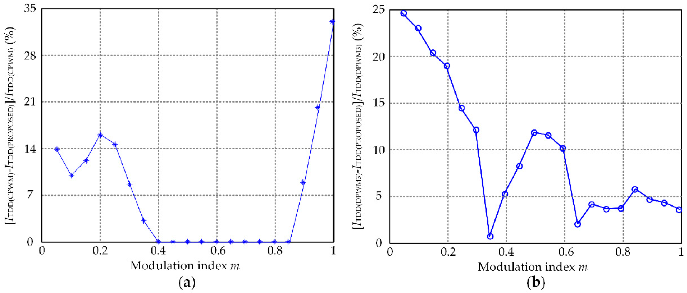
Figure 11b. The percentage improvement of proposed strategy versus CPWM and DPWM3 is shown in
Figure 12.
At the rated frequency (modulation index m = 1), ITDD of the proposed strategy drops 33% and 3.5%, respectively, compared with CPWM and DPWM3. Thus, the output waveform quality of the proposed strategy is improved.
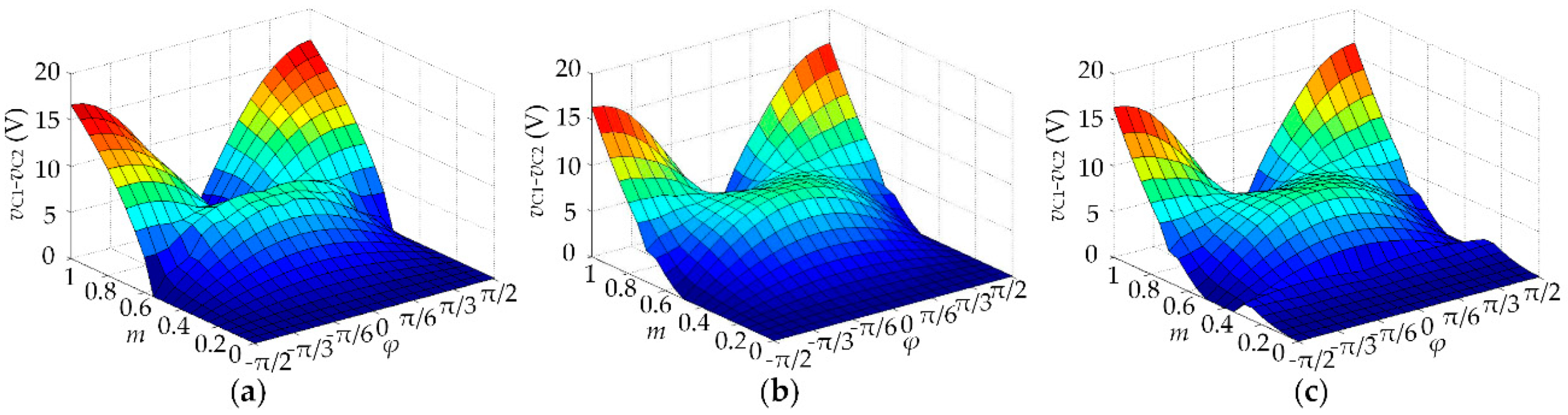
It is worth mentioning that the output waveform quality is also affected by the low frequency ripple in the neutral-point potential, as can be seen in
Figure 9 and
Figure 10. The dependence of neutral-point potential ripple
vC1-
vC2 on
m and power factor angle
φ for CPWM, DPWM3, and the proposed strategy can be calculated according to reference [
22], as shown in
Figure 13. The neutral-point potential ripple
vC1-
vC2 for CPWM, DPWM3, and the proposed strategy are approximately the same, so their effect on the output current ripple are the same, too.
6.2. Comparison of Power Losses
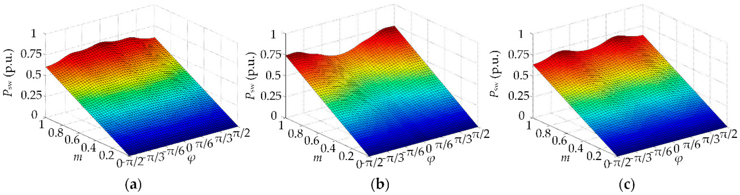
The switching losses of CPWM, DPWM3 and proposed strategy are calculated according to the method in reference [
23], and the dependence of switching loss on
m and power factor angle
φ are shown in
Figure 14.
As can be seen, when the power factor is close to 1, the switching loss of proposed strategy is lower than CPWM and a little bit higher than DPWM3. However in other cases, the switching losses of these three strategies are approximately the same.
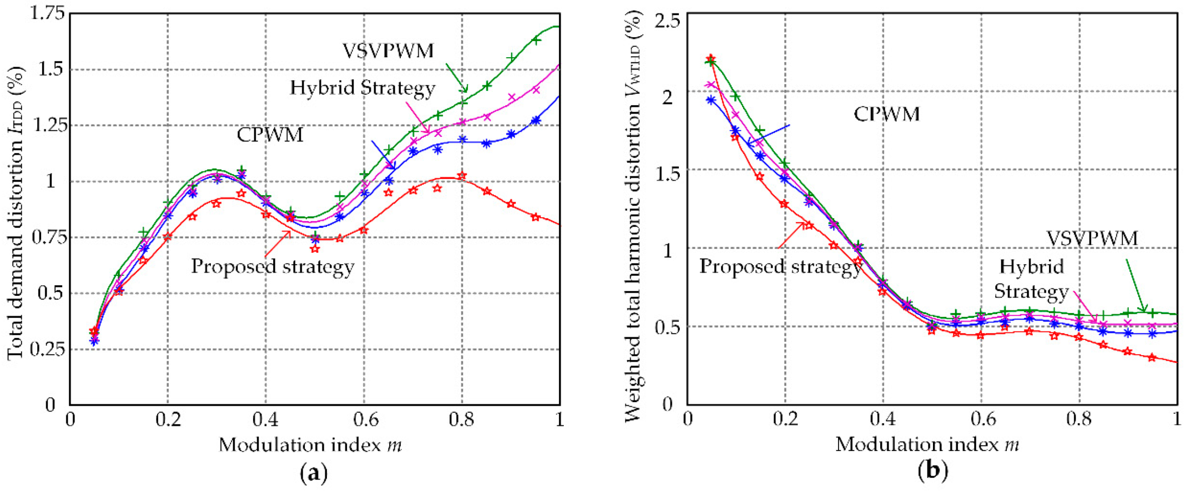
6.3. Comparison with Neutral Point Balancing Strategies
The dependence of
ITDD and
VWTHD on modulation index
m for CPWM with a neutral-point balancing control [
8], a virtual SVPWM (VSVPWM) [
11], a hybrid strategy of these two methods [
12] and the proposed method are shown in
Figure 15. As can be seen, when the modulation index
m > 0.1,
ITDD and
VWTHD of the proposed strategy is lower than the other three strategies. It can be concluded that the output performance of the proposed method is better than usual-adopted SVPWM with neutral-point potential balancing strategy and VSVPWM.


