1. Introduction
Recently, global problems such as population concentration in metropolitan areas, environmental pollution and global warming have led to the spread of renewable energy around the world. New and renewable energy sources are generally classified as distributed generation (DG) because they are small in capacity and distributed close to cities. When the DGs are connected into the grid, grid code parameters such as total harmonic distortion (THD) and reliability must be satisfied. The fault ride-through (FRT) regulation is one of the representative grid codes that define these requirements. According to the FRT regulation, the voltage dip of the grid should be suppressed by supplying reactive power when the DG is connected into the grid.
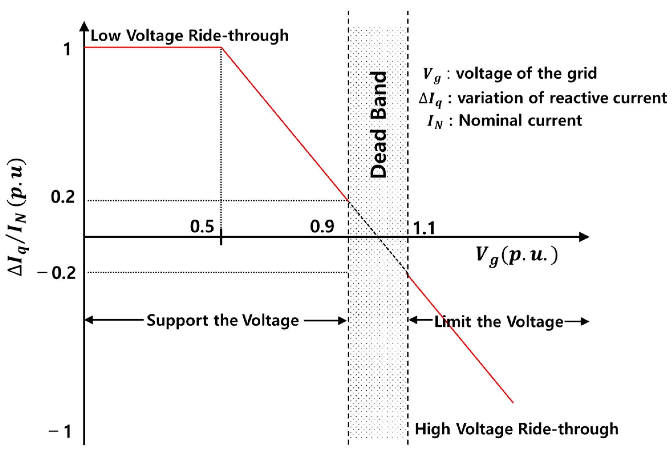
Figure 1 shows a graphical representation of the reactive current that is needed according to the grid voltage’s variation. When the grid voltage is between 0.9 and 1.1, it is called a dead band and the DG does not have to supply reactive current or reactive power into the grid. However, in regions other than the dead band, the reactive current from the DG between 0.2 and 1 p.u. according to the grid voltage should be supplied into the grid [
1].
The grid code that the reactive power should be supplied according to grid voltage is especially called as low or high voltage ride-through (LVRT, HVRT) regulation. As a method of suppressing the voltage-dip of the grid, a solution applying a superconducting fault current limiter (SFCL) has been reported [
2,
3,
4,
5]. The larger impedance of the SFCL is expected to provide a more effective suppression of the grid voltage. Another feature of the application of SFCLs is the reduction of the fault current, which can affect the operating time of the over-current relay (OCR). The OCR, which determines the trip time according to the magnitude of the fault current, sends the delayed trip signal to the circuit breaker because of the decrease of fault current. This trip delay interrupts the proper operation of the circuit breaker, which affects the protection coordination between the protective relays such as the OCR. Therefore, the resetting of the OCRs considering the application of the SFCL is required to keep the coordination time interval (CTI) between the OCRs [
6,
7,
8].
A SFCL with lower impedance can avoid affecting the trip delay of the OCR, however, the lower impedance of the SFCL can allow a larger reactive power to be supplied to the grid according to the LVRT regulation. Due to the characteristics of the converter, the increase of the reactive power supply causes a decrease in the active power supply. Reduction of the active power supply results in an unbalance between the input and output active powers in the DC link comprising the voltage source converter (VSC) system. This active power unbalance is a major cause for the rise of DC links’ voltage. In order to suppress the rise of the DC links’ voltage, the balanced operation of both the input and the output active powers in the DC link is needed. Previous solutions such as the deloading method and the installation of a chopper resistor have been suggested to suppress the DC links’ voltage rise due to this unbalance [
9,
10,
11,
12,
13].
The deloading method is a technique that reduces the active power into the DC link by reducing the active power through torque control of the DG [
9,
10,
11]. The deloading method should reduce the active power of the converter on the DG side at the same time as the torque control. However, this is only possible if the torque from the DG and the voltage from the converter are exchanged with each other instantaneously. For this purpose, an optical or wireless communication system considering the distance between the converter system and the DG is required, which is a financial burden for the system operator using this deloading method. Another method is where any excessive active power input into the DC link is dissipated through a chopper resistor installed on the DC link in parallel [
12,
13]. It is considered as the effective alternative because it is installed directly on the DC link and the transient response is much better than that obtained with the deloading method. However, the additional chopper resistor also needs to be installed directly on the DC link.
In this paper, as the method to suppress the voltage-dip of the grid, the application of SFCLs was considered and the FRT regulation due to the impedance of the SFCL was examined. In addition, to alleviate the rise of the DC-links’ voltage in the VSC due to the SFCL application, the active power tracking control (APTC) method was suggested. Through power system computer-aided design/ electromagnetic transient design and control (PSCAD/ EMTDC; Manitoba Hydro International, Winnipeg, Manitoba, Canada) simulation, the FRT capability of the power distribution system linked by the DG was confirmed to be enhanced by using the suggested APTC method considering the application of SFCLs.
2. Construction and Modeling
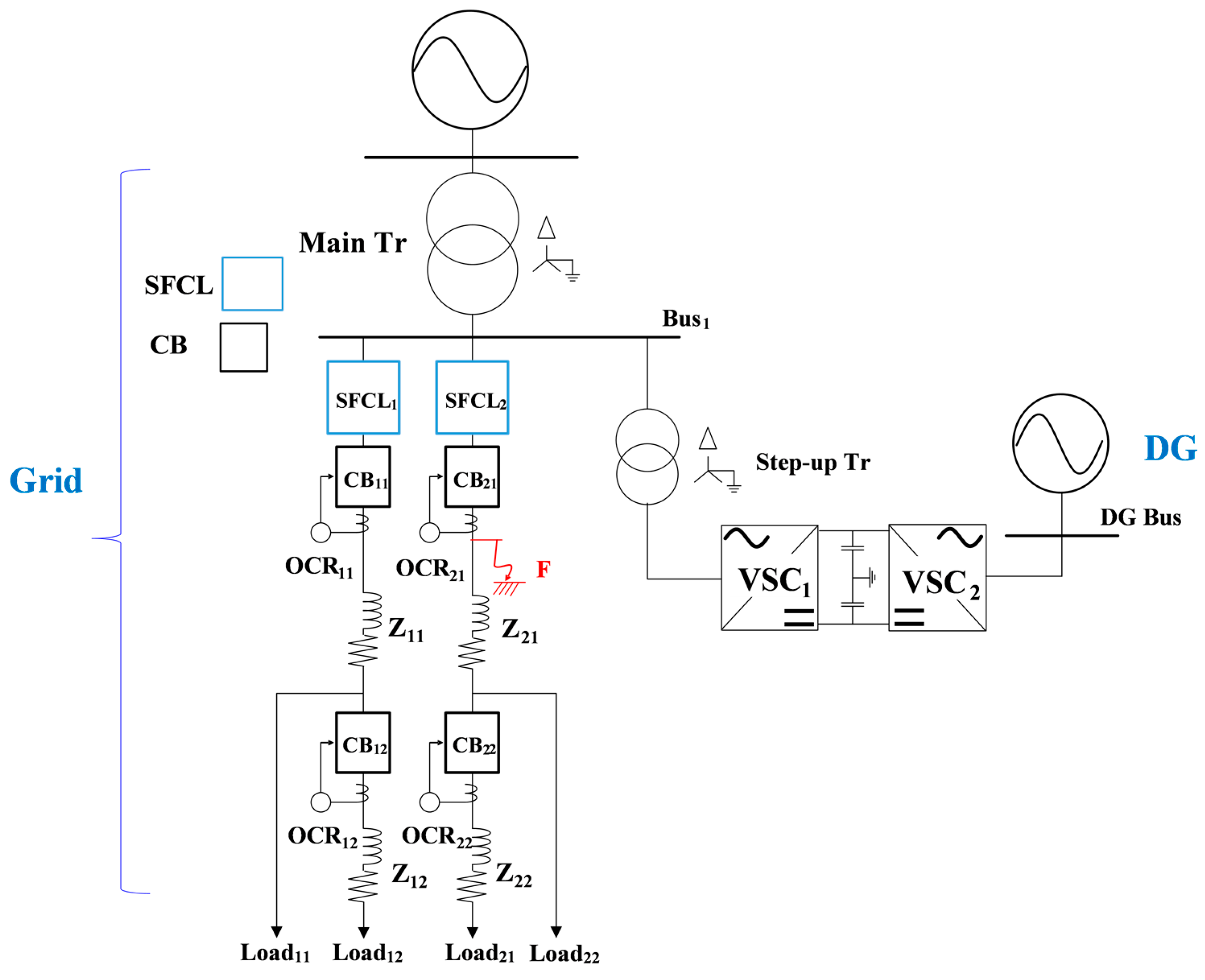
The construction of the power distribution system, examined in this paper, is similar to one connected with DG such as a wind farm through a DC link of more than 100 kV voltage except for the scale of the system voltage [
14,
15,
16,
17].
Figure 2 shows the configuration of the grid linked by the DG through the DC link of VSC systems. The grid consists of a power source and two feeders via a main transformer (Main Tr). Each feeder was constructed to be protected by the CBs, operated by OCR. In the output terminal of each feeder, the SFCL was installed to limit the fault current and to suppress the voltage-dip of the main bus line from the short circuit occurrence within the grid.
The DG is connected with the main bus line (Bus1) of the grid through the step-up transformer and the VSCs system. The DC link is the middle point between two VSCs, which converts AC voltage from the DG into DC voltage and then is converted to the AC voltage of the grid. Normally, the active power from the DG is transmitted into the grid through the control of the VSCs. With the consideration for each component’s operation, modelling of the VSCs, the SFCL and the OCR were performed. A short circuit fault was simulated at point F of the grid and the voltage drop of the grid was observed in the main bus line, which was the connection point of the DG with the grid. Additionally, the operations of the OCR due to the application of the SFCL were examined.
2.1. Modeling of VSC
The voltage of the DC-link in middle point between two VSCs needs to be a constant value. In other words, any increased or decreased voltage in the DC-link, which is related with the unbalance of the active power on either side of the VSC, must be kept to constant by the controlling the VSC. The global trend is aimed at using a multi-DC terminal where multiple AC/DC converters are connected to one another. Since the current source converter (CSC) system using the silicon controlled rectifier (SCR) has an inherent problem that it cannot control the reactive power and the active power independently, the VSC system using the insulated gate bipolar transistor (IGBT) or the gate turn-off thyristor (GTO) that independently control the reactive power and the active power has received more attention all over the world. These VSCs can selectively control the active power and the reactive power. "Selectively" means that the active power is physically related with the DC voltage and that the reactive power is physically related with the AC voltage. Therefore, one of them can be taken as the reference value to adjust the desired value [
18,
19,
20,
21].
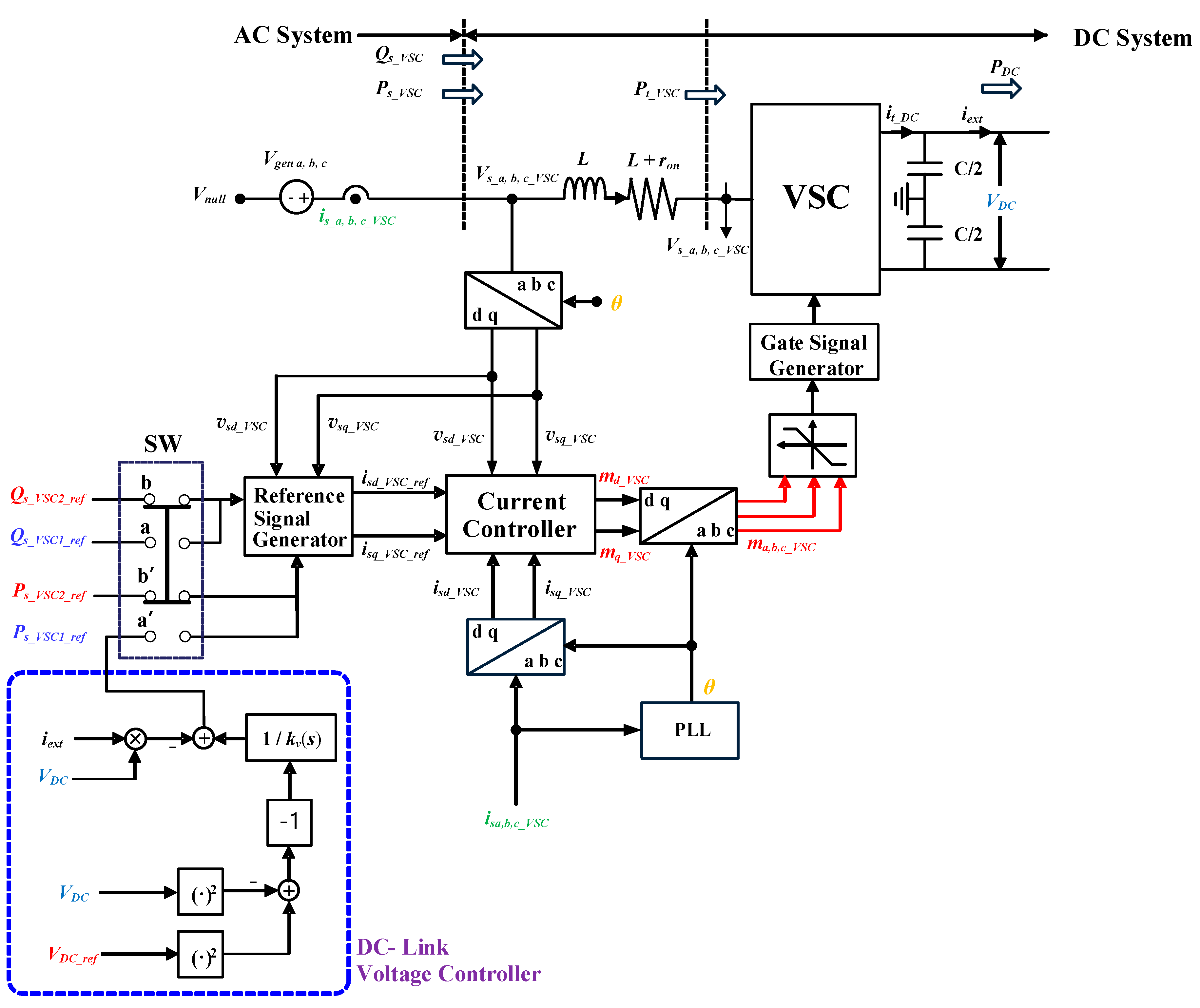
In the case of the VSC
1 in
Figure 2, the DC voltage (
VDC-Ref) for the active power (
PS_VSC1-Ref) and the reactive power (
QS_VSC1-Ref) are selected as the references as displayed in
Figure 3. The VSC
1 is controlled to supply the active power corresponding to the reference value of DC-link’s voltage into the grid. In the case of the VSC
2, the reference values (
PS_VSC2-Ref,
QS_VSC2-Ref) for the active power and the reactive power can be changed by SW as shown in
Figure 3. In
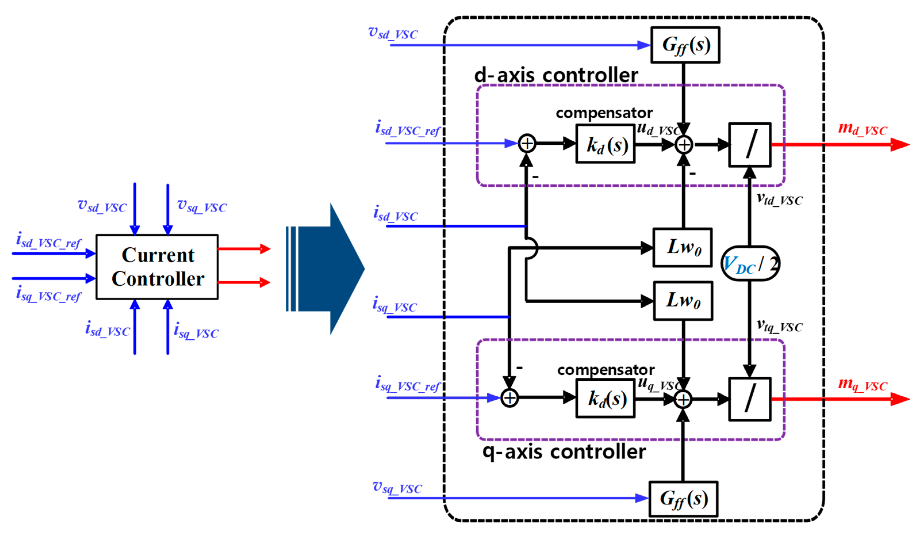
Figure 4, the internal circuit of the ‘Current Controller’ in
Figure 3 is designed.
As can be seen in
Figure 3, the input signal of the VSC (
ma,b,c_VSC) for the IGBT’s 3-phase pulse width modulation (PWM) is generated through the dq-abc frame-transform from
md_VSC and
mq_VSC. In addition, the current controller receives the dq-axis currents (
isd_VSC,
isq_VSC) and the dq-axis voltages (
vsd_VSC,
vsq_VSC) together with the dq-axis current references (
isd_VSC_Ref,
isq_VSC_Ref) and outputs the modulating signal (
md_VSC,
mq_VSC).
In this process, the control in dq-frame has the feature of reducing the number of necessary control loops from three to two. Additionally, the reference, feedback, and feed-forward signals in abc frame have generally sinusoidal functions of time. Therefore, to satisfy the desired transient response and the small steady-state errors, the compensators may need to be high order and the closed-loop bandwidths must be adequately larger than the frequency of the reference values. Consequently, the compensator design is not a simple task, especially if the operating frequency is fluctuating. If the control is carried out in the dq-frame, a sinusoidal reference tracking operation is transformed to an equivalent DC reference tracking one. Hence, the proportional-integral (PI) compensators can be properly applied for the control [
18].
The following Equations (1) and (2) are the formulas for generating the modulating signal in dq-frame. These equations can be derived from the AC side voltage equation from
Figure 3 and can be represented by the control block diagrams as shown in
Figure 4. The transfer functions (
Kd(
s),
Kq(
s)) of the current controller is equal to Equation (3), and the proportional gain and the integral time constant are specified in
Table A1:
The dq-axis current references (
isd_VSC_Ref,
isq_VSC_Ref) are generated through the reference signal generator with the input values of both the active power (
PS_VSC_Ref) and the reactive power (
QS_VSC_Ref) as shown in
Figure 3. The relationship between the active power (or, the reactive power) and the d-axis current (or, the q-axis current) is expressed in equations (4) and (5). As mentioned for the LVRT regulation in the introduction part, the q-axis current can be controlled to adjust the reactive power as seen in Equation (5) in case that the dip in the bus line’s voltage of the grid happens due to the short-circuit occurrence in the grid:
From Equations (4) and (5), if the bus voltage of the grid (
vsd_VSC) is constant, it is analyzed that the reactive power and the active power can be controlled by the d-axis current and the q-axis current, respectively, which is confirmed that the reactive power and the active power can be controlled independently. In addition, the relation of the DC-link’s voltage and the active power can be derived using Equation (6). A seen in Equation (6), the difference (
) between the charged and the discharged active powers in the DC-link is expressed with the transfer function (
) for the difference
) between the square of the DC-link’s voltage and the square of the reference DC-link’s voltage:
where subscripts ~ represents small perturbation of the variables.
represents the magnitude of
.
2.2. Modeling of Superconducting Fault Current Limiter (SFCL)
In the past three decades, many studies on the application of the SFCL to power systems have been reported and real field projects with SFCLs have been carried out. As the application model of the SFCL into power system, the resistive type SFCL, which consists of only a superconducting module (SCM) without other additional device, has been mostly considered because of its simple and compact structure [
22,
23]. However, in real field systems, during fault occurrence, the continuous flow of the larger fault current into the SCM may damage the SCM and take a longer recovery time to reach the superconducting state after the fault current is removed. These problems are related to the economic and the protective coordination issues.
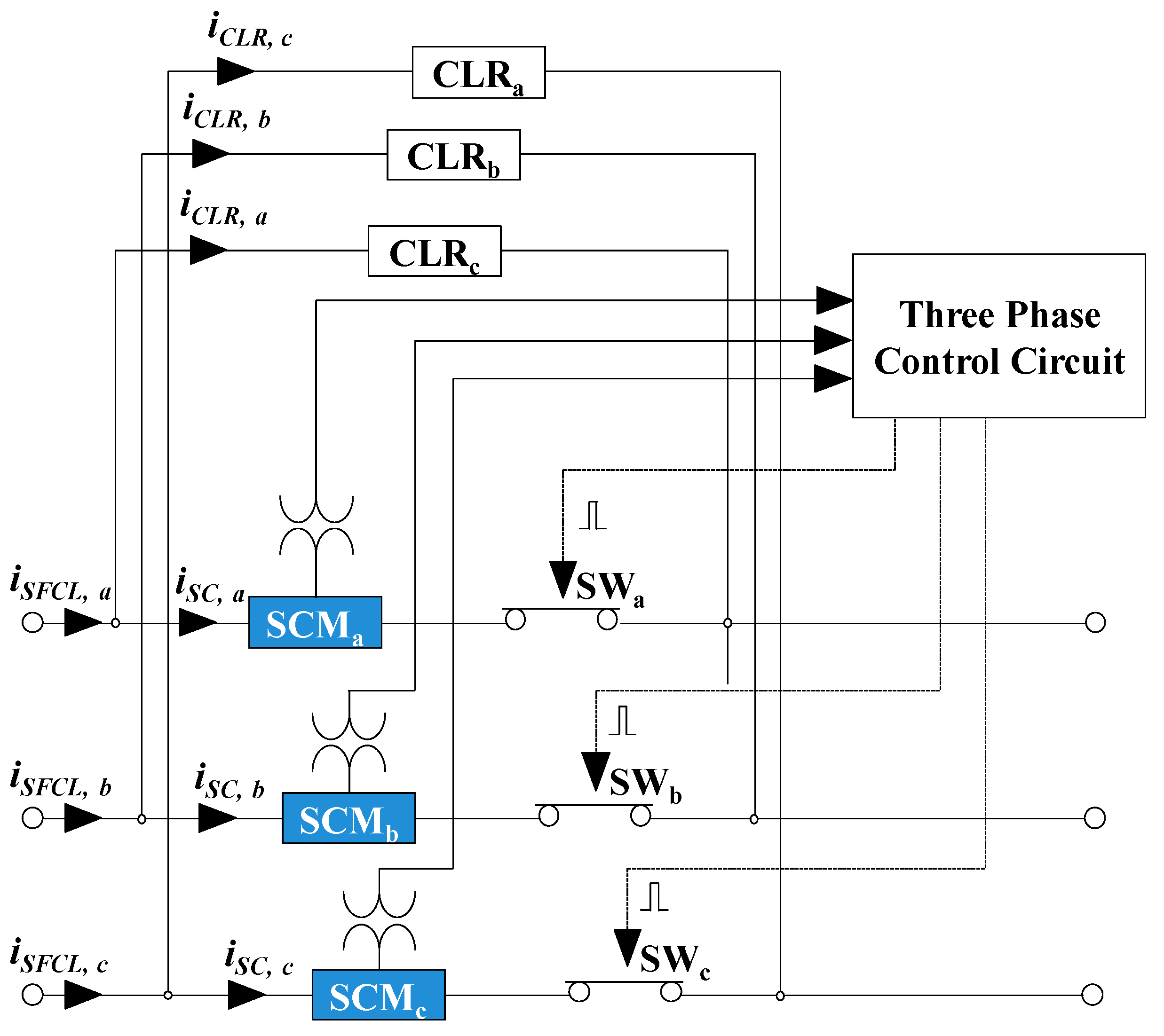
In this paper, as the SFCL model chosen to alleviate the above problems, a trigger type SFCL was considered. The trigger type SFCL consists of SCMs (SCM
a, SCM
b, SCM
c) connected in parallel with the current limiting impedances (CLR
a, CLR
b, CLR
c) and power switches (SW
a, SW
b, SW
c), such as the IGBT or the GTO, connected in series to the SCM as shown in
Figure 5. The control circuit in the trigger type SFCL sends the opening signal to the power switches if the induced voltages across the SCMs measured through the PTs exceed the setting voltage value and the SCMs can be separated from the fault current path.
Although the SCMs’ resistance generation comprising the trigger type SFCL is affected by the various physical parameters such as the magnetic field, the temperature and the current, the mathematical modeling of the SCMs’ resistance is performed with consideration for the current flowing into the SCM, as expressed in Equation (8), where
is the resistance that converges after the SCM is quenched, and
is the time constant [
24,
25]:
Since the current does not exceed the critical current of the SCM before the fault occurrence, the resistance of the SCM () is zero as expressed in Equation (8). However, in case that the exceeds the critical current of the SCM due to the short circuit occurrence, the SCM is quenched and changes into the normal state and the resistance of the SCM increases as described in Equation (8). As a result, the current is reduced and the is increased. If the voltage induced in the after the quench occurrence exceeds the voltage value which is set for the opening operation of the SW, the SW is opened by the opening signal from the control circuit. After the SW is finally opened, the fault currents flow into only the CLRs and the fault current is limited without the power burden of the SCMs by the CLRs.
2.3. Modeling of Over Current Relay (OCR)
The mathematical equation for the OCR’s operational characteristics was utilized by using Equation (9). In Equation (9), TD means time dial. A, B and p represent constant values to express the operational characteristics of the various OCRs. The M is a variable depending on the current (
through the OCR, measured by current transformer (CT) as expressed in Equation (10). The
is the presetting value that the OCR starts to calculate for its trip operation [
6]:
For the OCR to generate the trip signal at the Ttrip (trip time), calculated from Equations (9) and (10), the integration value (INT) is introduced in the operational modeling of the OCR. The definition of INT is equal to the sum of the reciprocal values of Ttrip in every sampling time. In case that the INT reaches ‘1’, the OCR sends the trip signal to the circuit breaker to open. As seen in Equation (9), Ttrip is determined by IP since all variables except for M are constants.
From Equations (9) and (10), it is expected that the operation of OCR can be delayed in case of the SFCL’s application due to its current limiting operation. To keep the original operational time of the OCR irrespective of the application of the SFCL, some methods such as the correction of the TD or the setting current (
) were proposed [
6,
7].
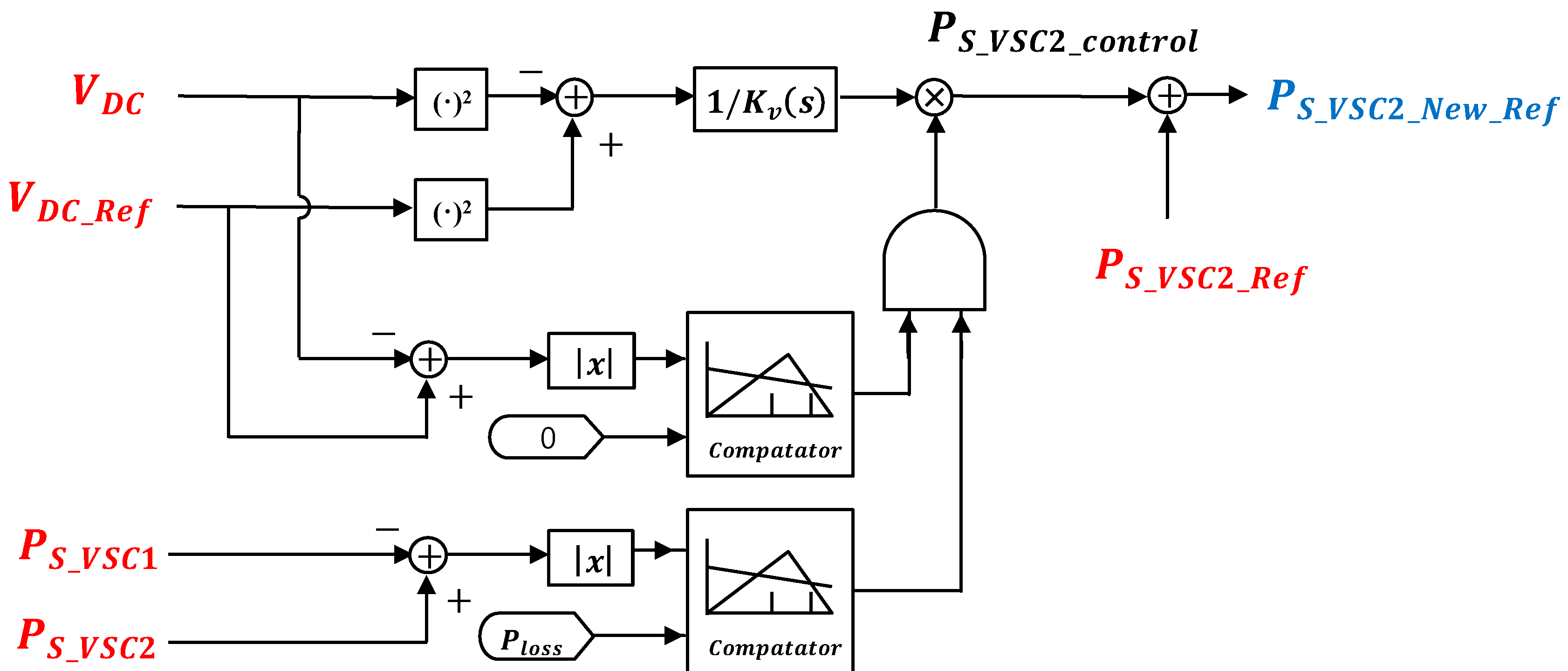
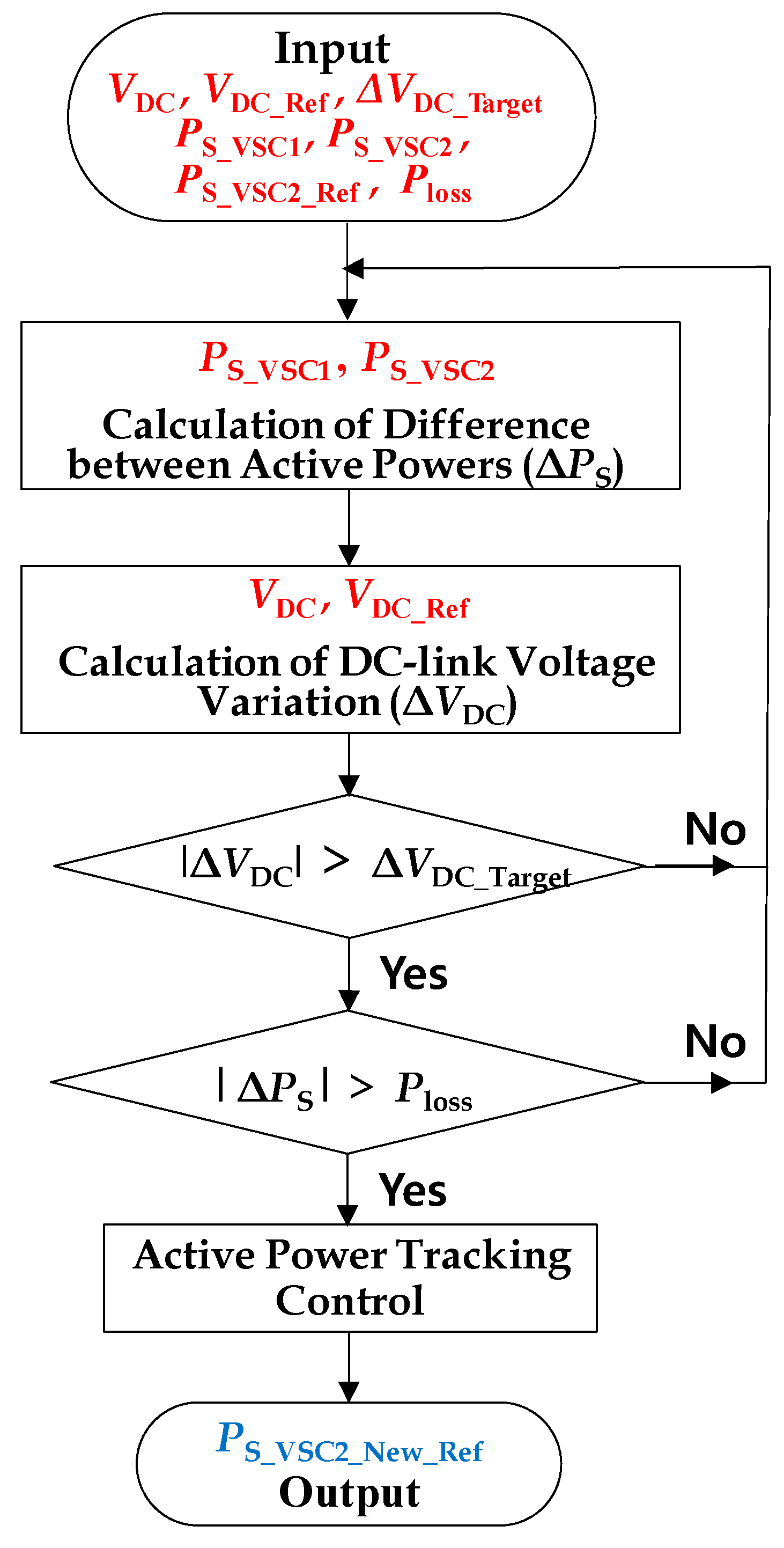
3. Active Power Tracking Control (APTC) for Suppression of DC-Links’ Voltage Rise
As explained in the Introduction, in case that an abnormal voltage occurs in the grid, the VSC system is required to supply or consume the reactive power according to the FRT regulation. Especially, in case that the short-circuit occurs in the grid, the VSC system linked by the DG through the DC link performs the supplying operation of the reactive power for the prevention of the grid’s voltage dip. On the other hand, the active power from the VSC system is less supplied and the power imbalance in DC-link results in the rise of its voltage.
Figure 6 is a block diagram of the proposed method, and its operation algorithm is shown in
Figure 7.
In this paper, as the method to suppress the voltage rising in DC-link due to the increase of the active power from the VSC system linked by the DG, the APTC method was suggested. In the APTC method, the new reference value of the active power (
) is generated by adding the active power’s control value (
) to the existing reference value of the active power (
) as shown in
Figure 6. The active power’s control value, which is calculated through the difference for the square calculation of both the DC-link’s voltage and the DC-link’s reference voltage, is only effective for the new reference value of the active power in both the cases; one is that the variation of DC-link’s voltage exceeds its preset variation. Another is that the difference of input/output active powers in the DC-link exceeds the power loss such as the cable and conversion loss. For the both cases, the VSC
2 system is operated to supply the decreased active power based on the APTC algorithm from the DG into the DC-link, which is contributed to suppress the rise of the DC-link’s voltage. The operational flowchart of the APTC algorithm, described in
Figure 6, is also shown in
Figure 7.
4. Results and Discussion
As a method of verifying the operation of APTC, we can use a simulation based on theoretical modeling. It is more accurate to construct experiment with hardware and an experimental grid and DG systems, but this is practically limited due to economic reasons.
In this study, a VSC
2 that operates APTC algorithm, connected to DG, was considered. The VSC
1 controls the DC voltage through the active power regardless of the fault, and the reactive power has the output of 0 [MVar] on normal state, but performs the FRT operation at the low voltage due to the fault. The FRT operation was modeled as shown in
Figure 1 LVRT region. As the voltage decreases by 0.1 p.u., the reactive current is supplied by 0.2 p.u.
The VSC2 controls the active power to 15 MW without any reactive power under un-fault state. However, when the voltage of the DC link rises due to the FRT operation of VSC1, the VSC2 performs the APTC operation. At the same time, the trigger type SFCL operates in the fault location of the power distribution system. If the fault continues, the circuit breaker is tripped by the OCR to remove the fault.
The simulation is divided into three parts to verify the proposed protection scheme. The cases are as follows:
with or without case about SFCL consisted of resistance CLR; 0.1–0.8 Ω
with or without case about SFCL consisted of inductance CLR; 0.1–0.8 Ω
case of APTC operation with SFCL
4.1. Simulation Setup
As indicated in
Figure 2, a three-phase short-circuit fault was simulated at location in F at 0.3 s. Simulation studies were carried out in EMTDC/PSCAD (Manitoba Hydro International, Winnipeg, Manitoba, Canada) and the parameters for simulation in a whole system are given in the
Appendix A. In the event of the fault, the voltage of the fault location (F) of the feeder drops to 0 V at 0.5 s. The current flowing through the feeder increases and the current through current transformer (CT) increases beyond pickup current of OCR. The modeling parameters for the SFCL and the OCR operation in the simulation are given in
Table A2.
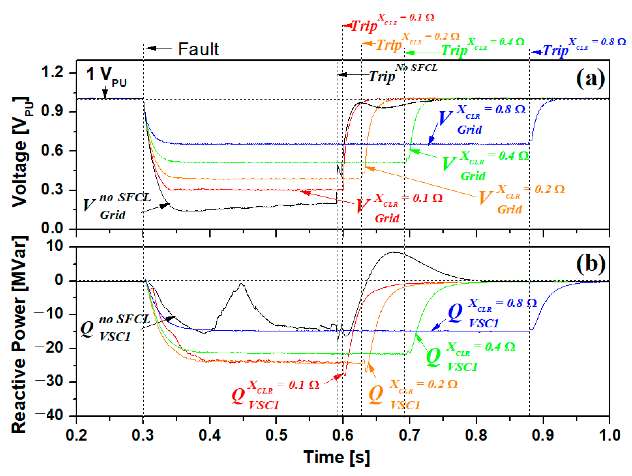
4.2. Protection of Distribution System (Operation of SFCL and FRT)
There is a 3-phase ground fault at the middle of the feeder, the voltage at the fault location becomes zero and the current increases greatly. The SFCL’s resistance is zero until the SCM is quenched, but when the SCM is quenched and SW is open, the SFCL’s resistance follows the set-up CLR impedance. In
Figure 8 and
Figure 9 below, the CLR impedance is changed from 0.1 to 0.8.
In
Figure 8 and
Figure 9, the grid bus voltage(
Vgrid,
Vsd_VSC1) is expressed in p.u. Also, the supplied reactive power(
Qs_VSC1) according to the grid bus voltage is shown separately as resistance CLR or inductance CLR. When the SFCL is not used, the operation of the VSC is abnormal because the grid bus voltage is excessively decreased. Therefore, it can be seen that reactive power has fluctuations. When a SFCL consisting of resistance CLR is applied, the reactive power also fluctuates but tracks the reference reactive power (
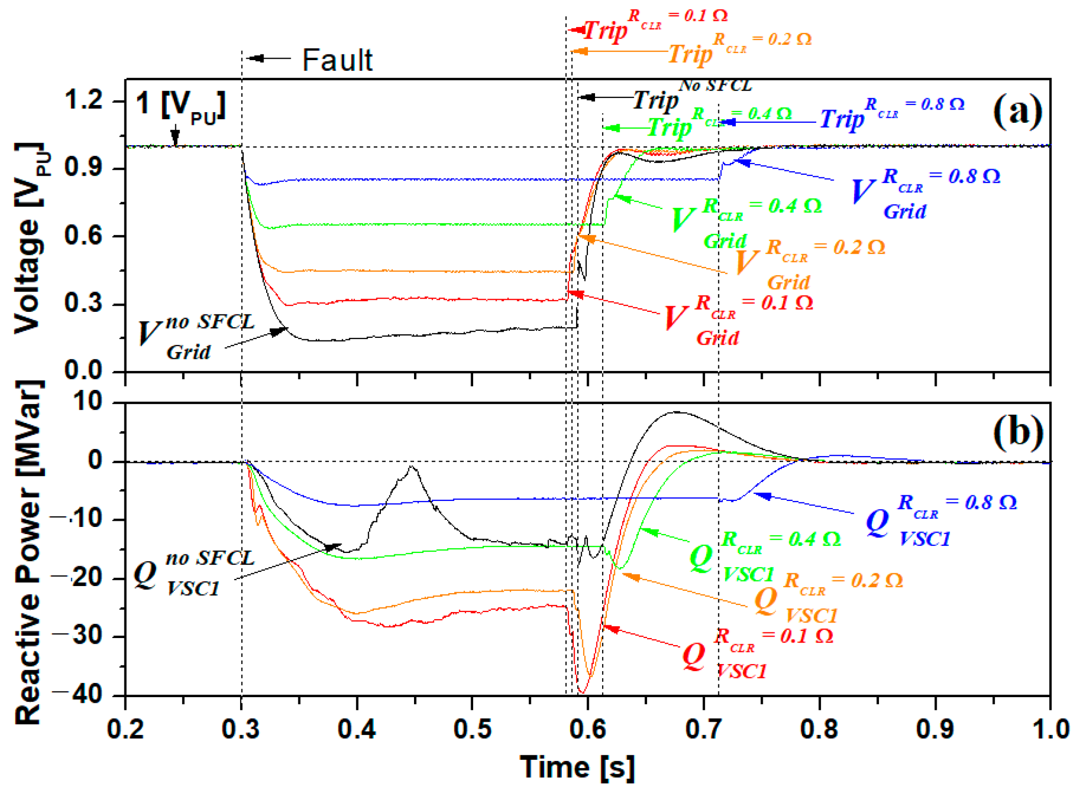
Qs_VSC1_ref). As the CLR impedance increases, the grid bus voltage-dip recovers, and less reactive power is supplied. However, if a SFCL consisting of inductance CLR is applied, it provides a stable supply with little reactive power fluttering. At this time, it can be seen that the longer the CLR impedance, the longer the trip time. The CLR inductance case was delayed more than the CLR resistance case.
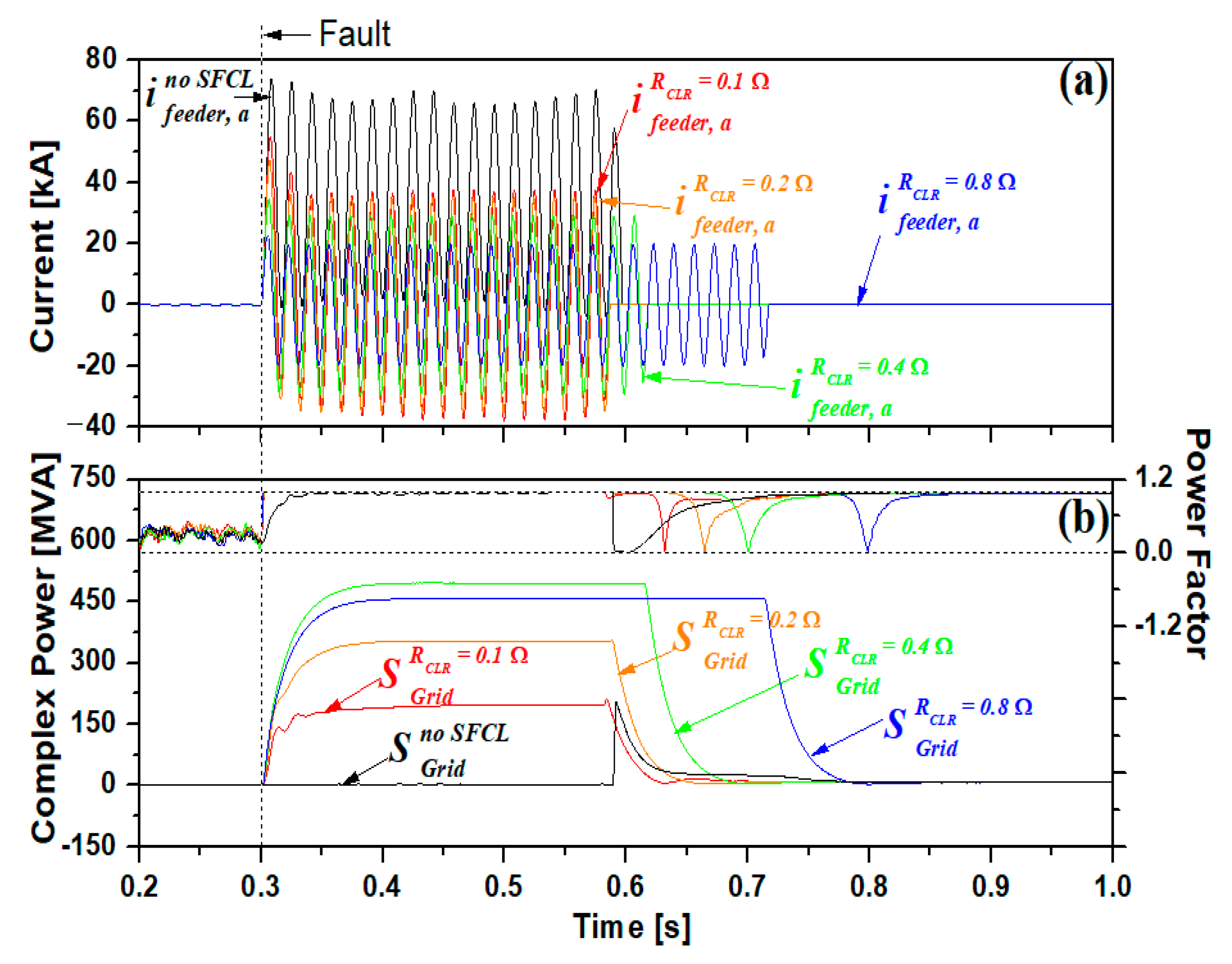
Figure 10 and
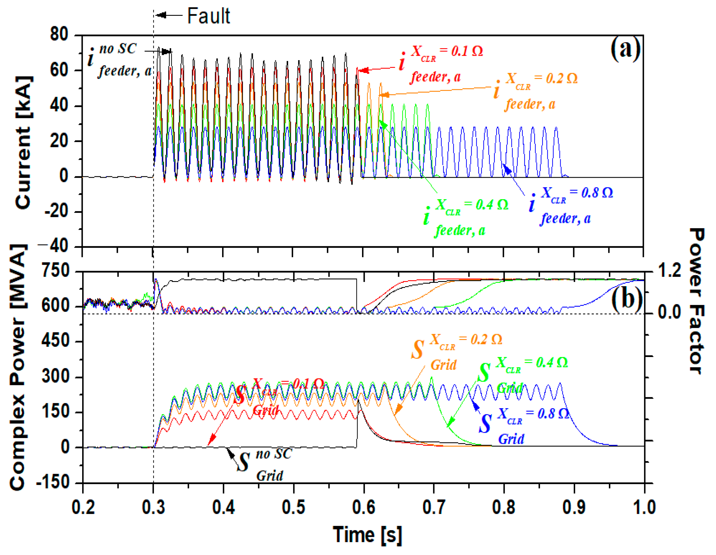
Figure 11 show the waveforms of current and complex power in the event of a fault in front of the feeder.
Figure 10 shows the CLR impedance of a trigger type superconducting fault current limiter (SFCL) with resistance.
Figure 11 is a graph where the CLR impedance consists of inductance. In the case of a resistance, it can be seen that the DC component of the current occurs and disappears at the beginning of the fault. It disappears when the fault continues because it is the DC component caused by the fault angle. However, when the CLR impedance is inductance, the current of the generated DC component is maintained. The peak value of the current is similar to that of the resistance, but it can be checked that the current does not fall below zero.
As shown in
Figure 8 and
Figure 9, the smaller the CLR impedance of the SFCL, the more reactive power the VSC1 was supplied. As the reactive power of VSC1 increases, the active power of VSC1 should decrease further. Because, converter has a limited amount capacity of complex power. When reactive power is supplied, if the amount of active power is not reduced, the VSC may be overloaded and the converter may be damaged.
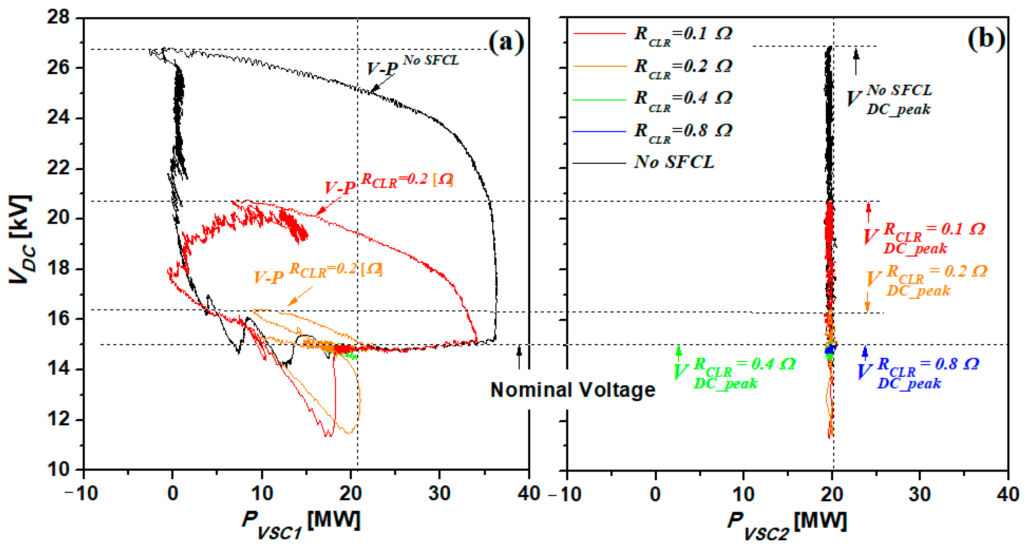
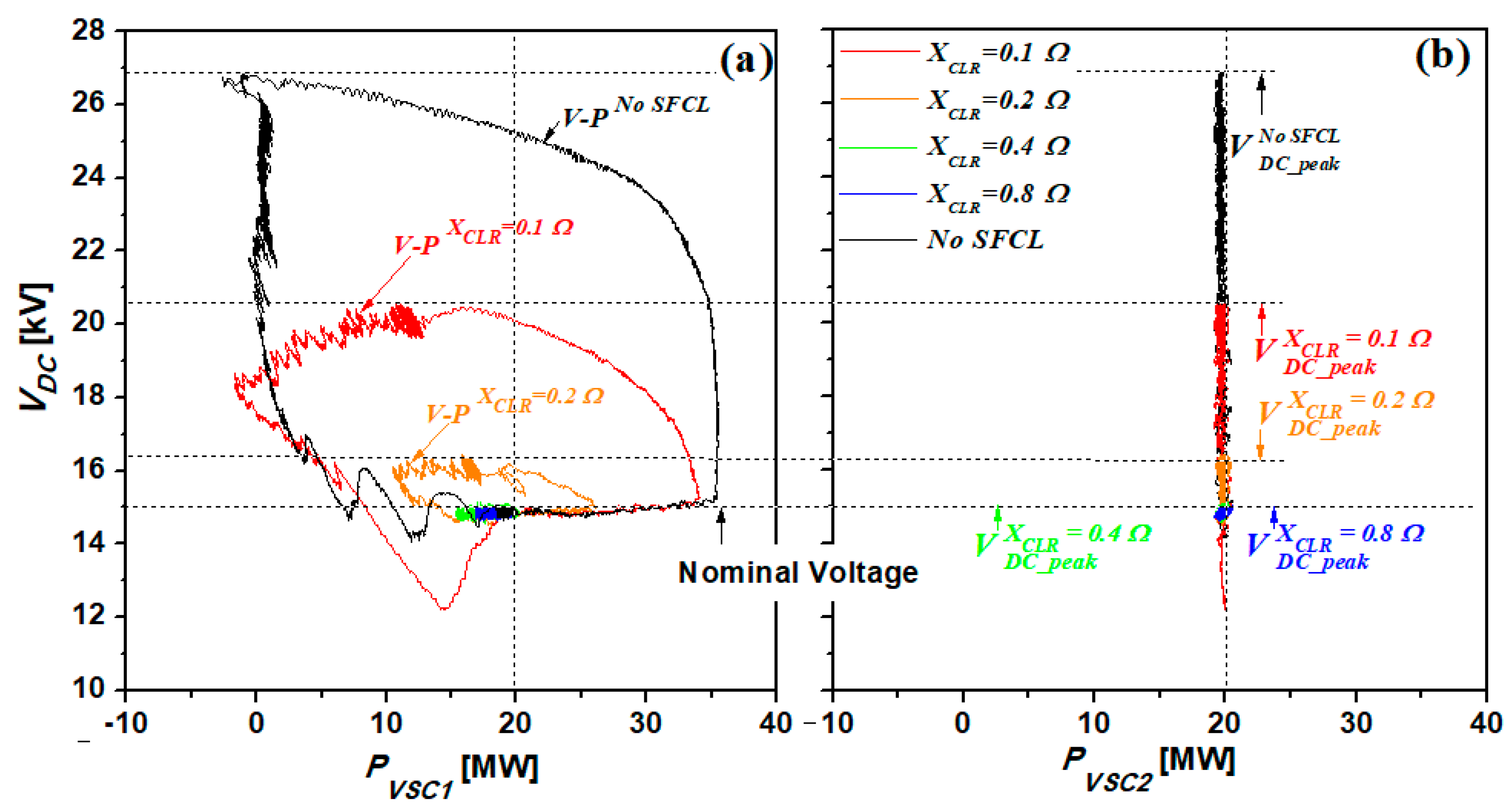
Figure 12 shows the P-V
dc curve when SFCL and FRT operation are applied. In
Figure 12a, the active power of VSC1 decreases when reactive power is supplied. In contrast, in (b), the active power of VSC2 is constant regardless of fault. Therefore, the smaller the CLR impedance, the higher the DC-link’s voltage. If the CLR impedance is an inductance, as shown in
Figure 13, the overall rise of the DC-link’s voltage is small.
4.3. APTC Operation
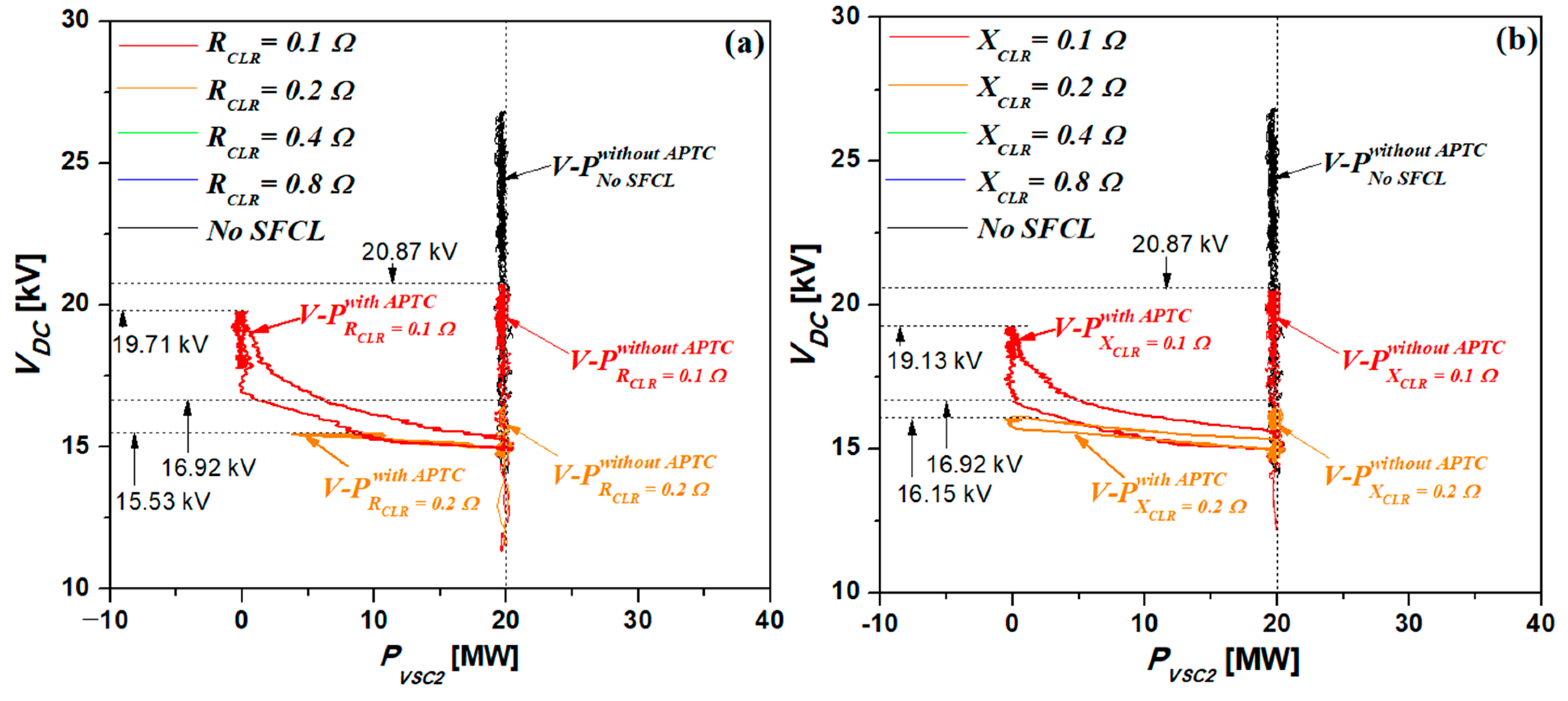
Previously, the smaller the CLR impedance, the higher the DC-link’s voltage.
Figure 14 shows the application of APTC. If APTC is not applied, it can be seen that the active power of VSC2 constant and DC-link’s voltage increases up to 20.87 kV. However, when APTC is applied, in resistance CLR case, the active power of VSC2 decreases rapidly to zero. The DC-link’s voltage rise is then suppressed to 19.71 kV or 15.53 kV, depending on the magnitude of the impedance. In the case of inductance CLR impedance, it is suppressed to 19.13 kV and 16.15 kV, respectively.
4.4. Discussion About Enhancement of FRT Capability
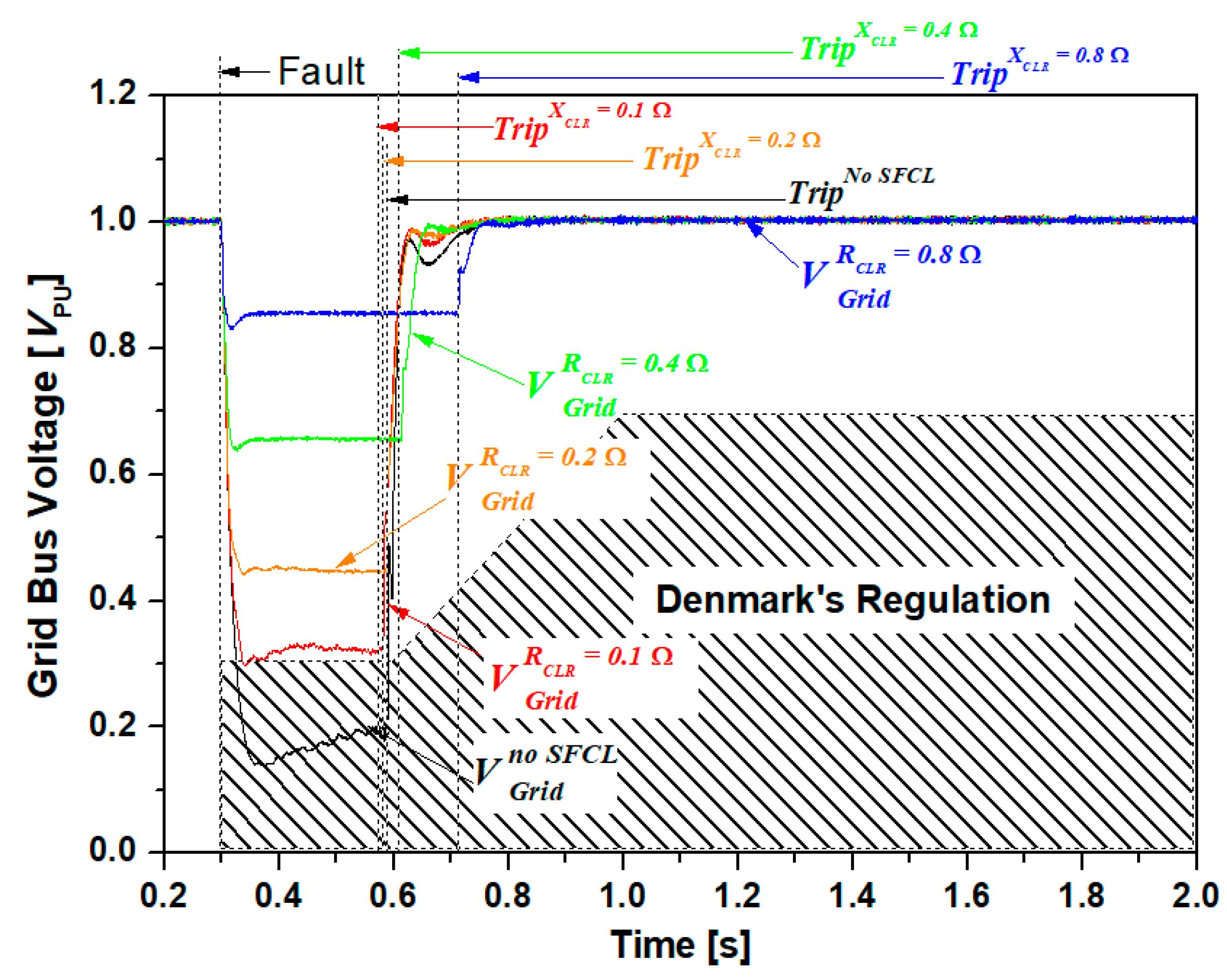
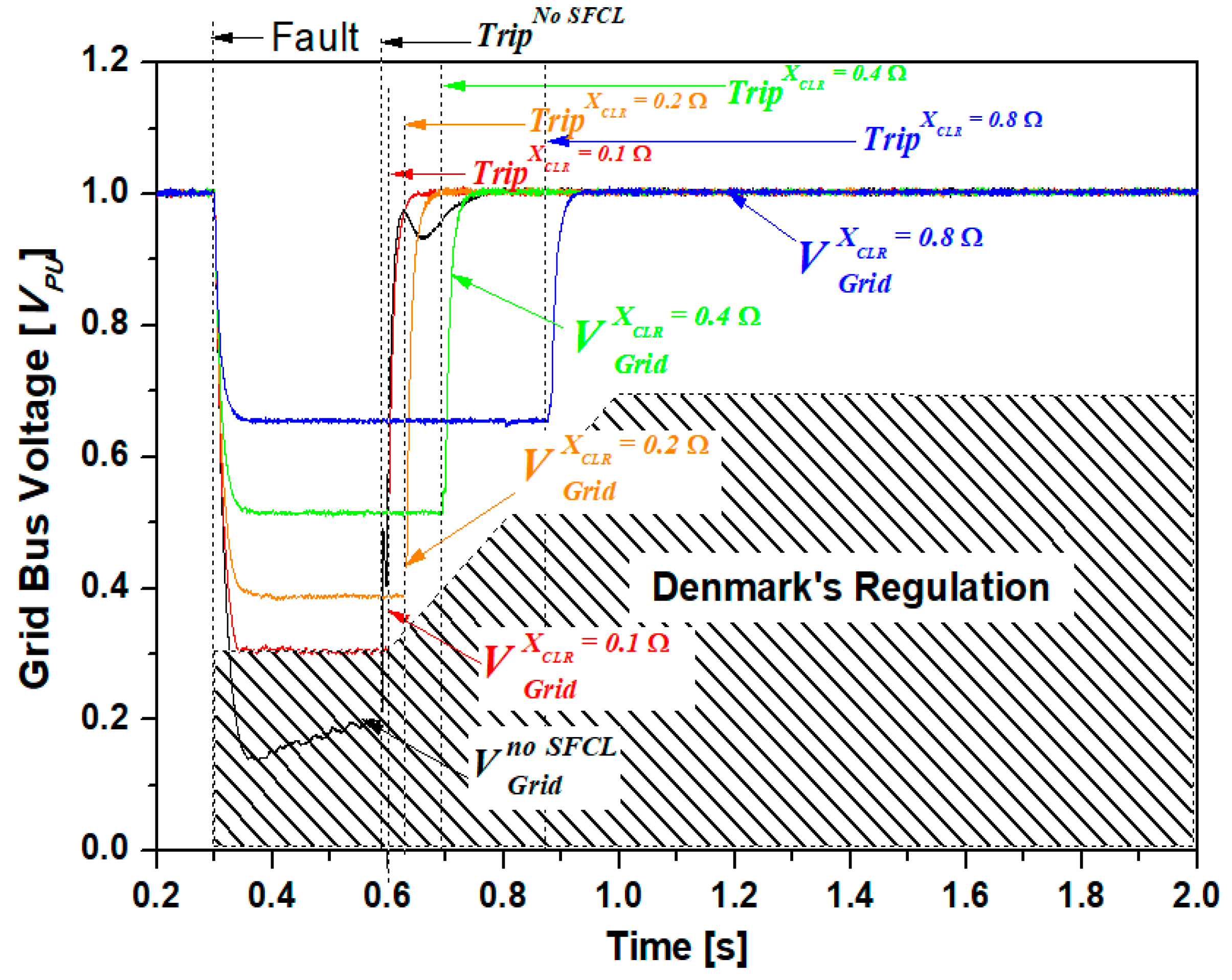
In the distribution system, the system protection proceeds using SFCL and OCR. And FRT operation is proceeded due to the grid bus voltage-dip in the VSC1. In
Figure 15 and
Figure 16, the grid bus voltages are plotted according to the type of CLR impedance. When the CLR impedance is a resistance, the grid bus voltage-dip can be effectively recovered with little trip delay even when the impedance is increased. In the case of not applying SFCL and applying SFCL with an impedance of 0.2, the grid bus voltage-dip recovered 0.33 V
p.u. and the trip delay was within 0.01 s. When the CLR impedance is inductance, the overall recovery of grid bus voltage-dip is small, and the trip delay is long. In case of applying SFCL with 0.2 impedance, voltage recovery was 0.28 V
p.u. and trip time delayed by 0.2 s. In each case, the DC-link’s voltage rose smaller when the CLR impedance was inductance than resistance case. However, when APTC was applied, it is effective about suppressing of DC-link’s voltage rise irregularly, regardless of the type of CLR impedance.
5. Conclusions
In this paper, the protection operation of power system in which DG and distribution system are connected via DC link is studied. When the fault occurred, the grid bus voltage-dip causes VSC1 to perform FRT operation, which caused the DC-link’s voltage to rise. At this time, if the SFCL is applied, the DC-link’s voltage rise is suppressed because the grid bus voltage-dip is recovered, and less reactive power is supplied through the FRT operation. The type and magnitude of CLR impedance were changed and APTC was applied to comprehensively examine the grid bus voltage-dip, trip delay and DC-link’s voltage rise. This paper analyzed the factors that reduce the system reliability when distributed power supply is connected to distribution system, and also analyzed the correlation between SFCL protecting AC system and control method protecting DC link. Therefore, this paper contributed to improving the reliability of AC / DC linkage power system. Following points are confirmed in this paper:
When designing the SFCL, it is hard to protect the superconducting element. Therefore, adding SW to the superconducting element and connecting the CLR in parallel with these, the superconducting element can be protected, and the limiting impedance can be increased.
Using the trigger-type SFCL, the FRT capability could be enhanced while protecting the SCM. As CLR impedance of SFCL increased, FRT capability improved but trip time delayed. When CLR impedance is resistance, FRT capability enhancement and trip delay performed best.
The APTC is effective at suppressing DC voltage rise. It is also more economical than other techniques because it does not require installation to suppress the DC-link’s voltage and long-distance communication devices.
Resistance CLR type SFCL was used and APTC technique was applied, FRT capability, trip delay and DC link suppression were effective.
Further consideration will be given when CLR impedance is used for both resistance and inductance. It will also be verified on an experimental system. On the other hand, the operation of the trigger type SFCL delayed the trip time of the overcurrent relay (OCR), and the OCR index correction is needed to solve this problem.


