Article

Compact Modeling of a 3.3 kV SiC MOSFET Power Module for Detailed Circuit-Level Electrothermal Simulations Including Parasitics

by
Ciro Scognamillo
1,
Antonio Pio Catalano
1,
Michele Riccio
1,
Vincenzo d’Alessandro
1,
Lorenzo Codecasa
2,
Alessandro Borghese
1,
Ravi Nath Tripathi
3,
Alberto Castellazzi
3,*,
Giovanni Breglio
1 and
Andrea Irace
1
1
Department of Electrical Engineering and Information Technology, University Federico II, 80125 Naples, Italy
2
Department of Electronics, Information and Bioengineering, Politecnico di Milano, 20133 Milan, Italy
3
SP2-Lab, Faculty of Engineering, Kyoto University of Advanced Science, Kyoto 6168577, Japan
*
Author to whom correspondence should be addressed.
Submission received: 26 June 2021 / Revised: 26 July 2021 / Accepted: 30 July 2021 / Published: 2 August 2021

Abstract

:
In this paper, an advanced electrothermal simulation strategy is applied to a 3.3 kV silicon carbide MOSFET power module. The approach is based on a full circuital representation of the module, where use is made of the thermal equivalent of the Ohm’s law. The individual transistors are described with subcircuits, while the dynamic power-temperature feedback is accounted for through an equivalent thermal network enriched with controlled sources enabling nonlinear thermal effects. A synchronous step-up DC-DC converter and a single-phase inverter, both incorporating the aforementioned power module, are simulated. Good accuracy was ensured by considering electromagnetic effects due to parasitics, which were experimentally extracted in a preliminary stage. Low CPU times are needed, and no convergence issues are encountered in spite of the high switching frequencies. The impact of some key parameters is effortlessly quantified. The analysis witnesses the efficiency and versatility of the approach, and suggests its adoption for design, analysis, and synthesis of high-frequency power converters in wide-band-gap semiconductor technology.

1. Introduction

The power electronics market is driving an exploding increase in demand for high-performance power circuits pervading fields like automotive [1], avionics [2], and renewable energies [3]. An increasing attention is attracted by wide-band-gap power devices, e.g., silicon carbide (SiC) MOSFETs, by virtue of their enhanced ratings in terms of switching speeds and frequencies, as well as higher operational temperature capability, as compared with e.g., silicon (Si) IGBTs [4,5]. In this scenario, most of the designers’ efforts have been oriented to develop advanced packaging techniques to follow the device-level progress [6]. This has led to the successful fabrication of multichip power modules (PMs) based on SiC MOSFETs, an example being presented in [7] for 3.3 kV VDMOS transistors; for this voltage class, the applications of which are the railway traction and wind power conversion, the replacement of Si with SiC is expected to have relevant benefits that allow justifying the higher technology cost. SiC PMs represent a breakthrough with respect to PCB-integrated power circuits [8] and are prone to be incorporated in any kind of converter topology; on the other hand, they require a careful design to efficiently handle (i) the considerable power density dissipated by devices and (ii) their high switching frequency [9]. Consequently, PM designers should pay attention to electrothermal (ET) effects and impact of parasitics [10,11].
In order to investigate the ET behavior of electronic devices/circuits, various approaches have been proposed in literature. Commonly-adopted strategies rely on the coupling of a SPICE-like circuit simulator and a 3-D thermal-only numerical software package (e.g., COMSOL Multiphysics, ANSYS) in a relaxation procedure [12,13,14]; however, this solution is onerous in terms of CPU time and memory storage, as well as prone to convergence problems. TCAD simulation tools (e.g., Sentaurus, ATLAS) allow simultaneously solving the semiconductor and heat flow equations within the same framework [15,16]; the huge computational burden required, however, makes their adoption only suitable for static device-level simulations [17].
As an alternative to methods based on numerical tools, we have developed an in-house approach based on a fully circuital representation of the whole device/circuit for self-consistent static and dynamic ET simulations with SPICE-like programs; considerable efficiency is gained with respect to [12,13,14] since the thermal problem is modeled with an equivalent thermal network derived through an advanced model-order reduction algorithm. The approach has been successfully used for devices/circuits in large variety of technologies, like an IGBT-based boost converter [18], a multicellular SiC power MOSFET operating under harsh conditions [19], and InGaP/GaAs HBT arrays for power amplifiers [20].
In [21], we have applied this advanced simulation strategy also to a 30 kW synchronous step-up DC-DC converter incorporating the 3.3 kV SiC MOSFET PM presented in [7]. Nonlinear thermal effects dictated by the high-power densities were accounted for; moreover, improved accuracy was ensured by the inclusion of parasitics, which were experimentally estimated through an electromagnetic characterization of the assembly. The circuit behavior was successfully described in spite of the high switching frequencies. In the light of the above considerations, this approach has the ambition of proposing itself as a valuable aid in the design flow of SiC-based PMs.
This paper is aimed to extend [21] in a four-fold way: (i) a deeper insight into the PM technology under analysis is presented; (ii) the architecture of the electrical subcircuit modeling the individual VDMOS transistor is explained, with emphasis on the temperature-dependent parameters; (iii) the inclusion of nonlinear thermal effects is thoroughly described; (iv) the suitability of the approach even for AC ET simulations is proven by applying it to a high-power inverter incorporating the PM under investigation.
The remainder of the paper is outlined as follows. In Section 2, the technology for the fabrication of the PM is described. Section 3 probes into the methodology adopted for the ET modeling and experimental characterization of the assembly; more specifically, details about (i) the parasitics extraction, (ii) the SPICE-compatible VDMOS electrical model with temperature-dependent parameters, and (iii) the thermal modeling of the assembly including nonlinear thermal effects are provided. In Section 4, the presented approach is applied to a step-up converter and a single-phase inverter, both embedding the PM under investigation. Simulation times, convergence capability, and suitability to parametric analyses are discussed. Conclusions are then drawn in Section 5.

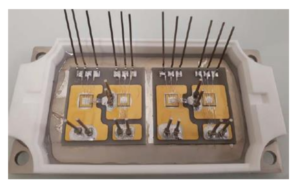
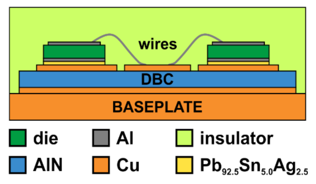
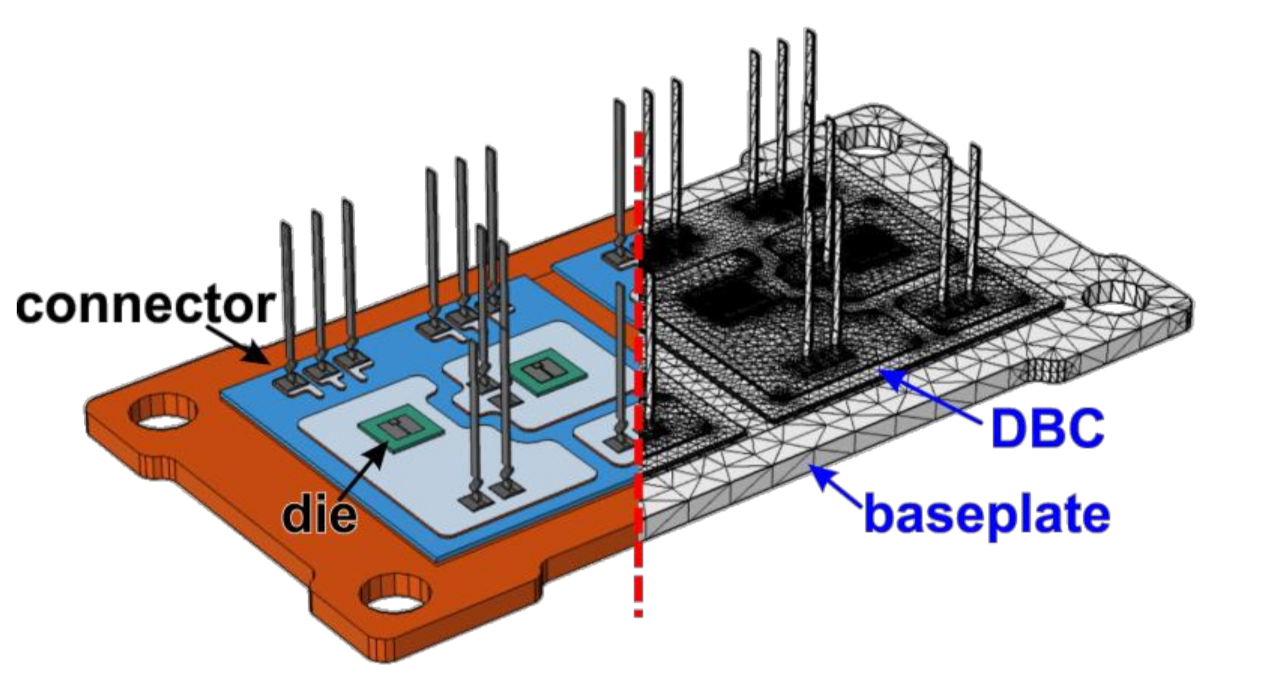
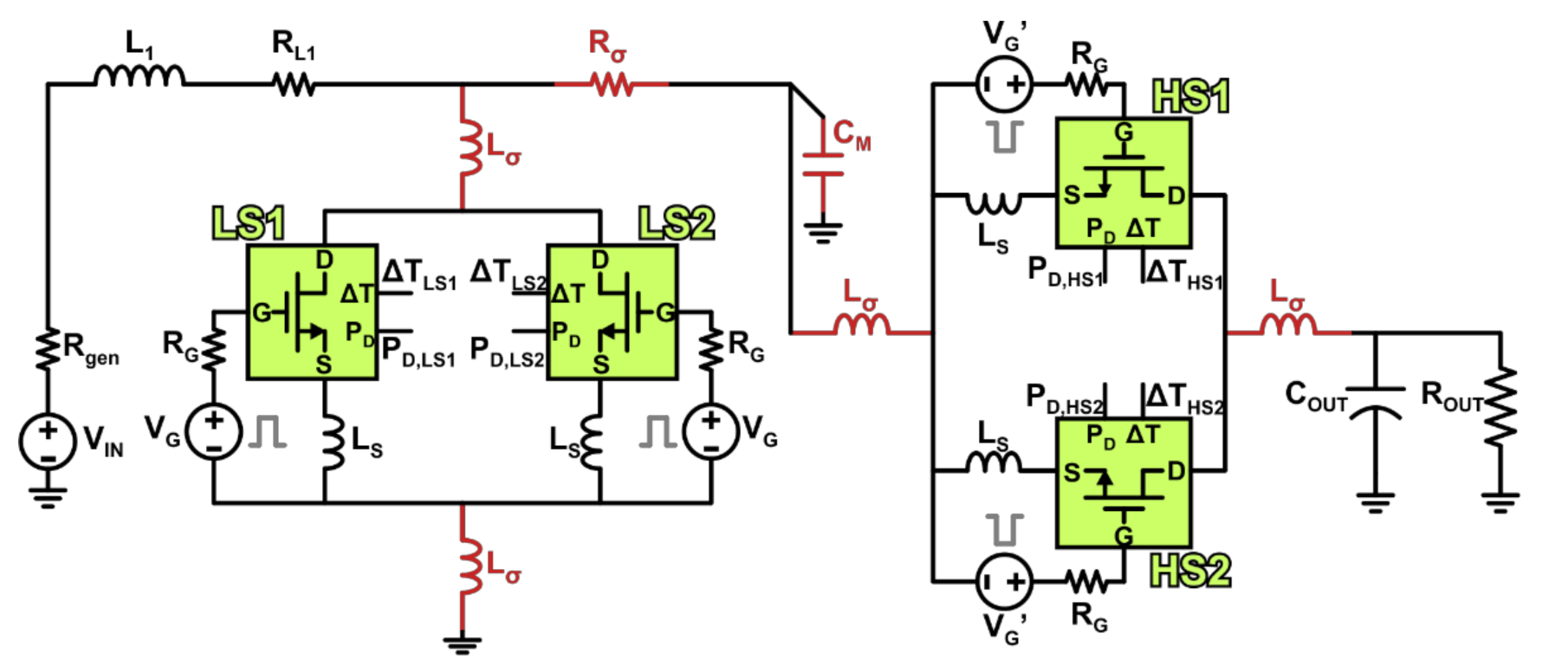
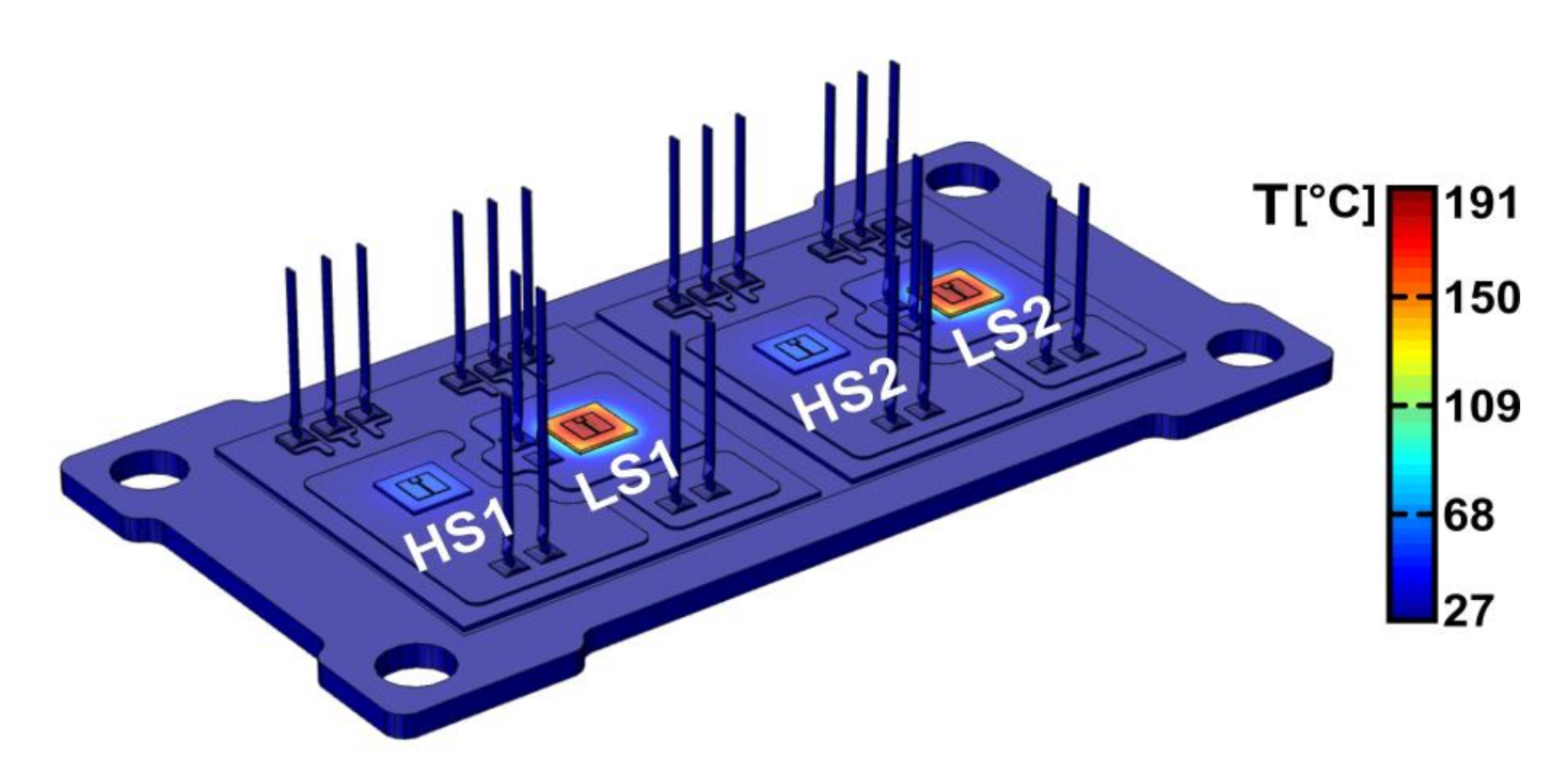
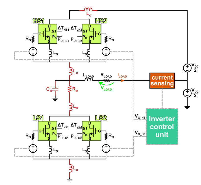
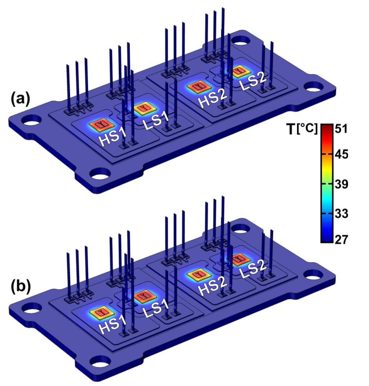
2. Power Module under Investigation

The general-purpose approach presented in this work is applied to a state-of-the-art PM characterized by two couples of SiC-based VDMOS transistors capable of withstanding up to 3.3 kV/50 A. Although the four devices can be used to realize a full H-bridge, here they are arranged in a half-bridge configuration with a doubled current rating. The assembly—compatible with standard PCB mounting processes [22]—is shown in Figure 1, while its schematic cross-section is represented in Figure 2. Each die is 7.2 × 7.2 mm2-large and 0.4 mm-thick and contains one transistor; the two VDMOS couples lie on two separate 40 × 40 mm2-large and 1.34 mm-thick direct-bonded copper (DBC) substrates. The DBC consists in a sandwich-like structure made of an electrical insulator sheet in between two copper (Cu) foils [23]. Many ceramic materials can in principle be adopted in the DBC manufacturing process. As shown in [23], the choice of the DBC technology has to be based on the application. For the PM under investigation, aluminum nitride (AlN) was chosen by virtue of its relatively high thermal conductivity and electrical resistivity. Concerning the Cu foils, the bottom one is kept plain to ensure a good thermal contact with the 3 mm-thick baseplate underneath (also made of Cu), while the layout of the top one is composed by metal islands in order to realize the circuit topology. The baseplate (i) provides mechanical stability to the assembly and (ii) improves the heat exchange between the devices and the cooling system placed underneath [9]. Electrical interconnections between Cu islands and devices are granted by aluminum (Al) wire bonds. An insulating gel is poured over the entire top surface in order (i) to increase the dielectric integrity and (ii) to avoid undesirable effects such as partial discharge and dielectric breakdown [24]. For the PM under analysis, a 5 mm-high silicon gel produced by Sylgard was considered [25]. Since the module PADs are covered by the insulating gel, Al vertical connectors are required to make them accessible.

3. Methodology

The simulation approach relies on the construction of a SPICE-compatible macrocircuit that models and fully couples the thermal and electrical behaviors of the PM under analysis. Such a macrocircuit also includes experimentally extracted parasitics. The individual VDMOS transistors are described with a behavioral subcircuit, the temperature-sensitive parameters of which are allowed to vary during the simulation run. The power-temperature feedback is accounted for with an equivalent thermal network extracted with low computational burden by means of a model-order reduction technique.

3.1. Parasitics Characterization of the Power Module

A preliminary study was devoted to the electromagnetic characterization of the PM parasitics. It consisted in the experimental evaluation of stray inductances, distributed resistances, and parasitic capacitances by varying frequency. To this aim, a Hioki IM3570 impedance analyzer [26] equipped with Hioki L2000 probes was exploited to measure the total loop parasitic inductance and resistance, as well as the common-mode capacitance. Results are shown in Table 1, which summarizes the values of the parasitics at the devices switching frequencies (fSW) of interest for the case-studies investigated in Section 4. It is worth noting that, during the parasitics measurements, the devices were fully-on (VGS = 20 V) and the total loop parasitic resistance was evaluated by subtracting the devices on-state resistance (~62 mΩ) from the measured value. The parasitic extraction did not take into account the coupling between inductance loops since the PM was designed so as to make such a mutual effect negligible [7].

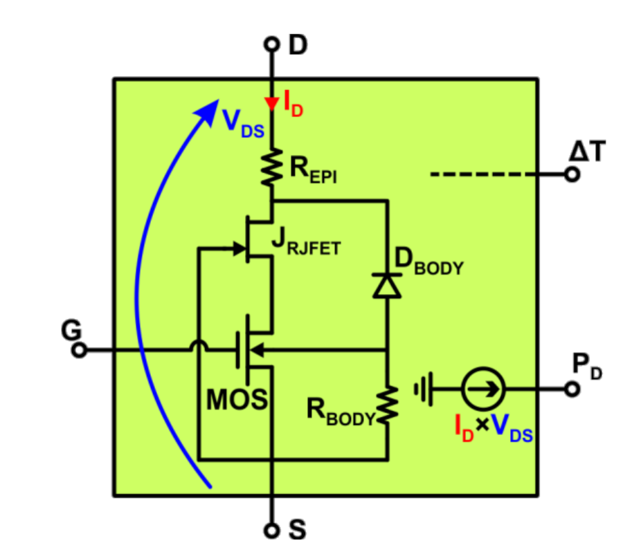
3.2. Electrical Model of SiC VDMOS Transistors

The compact electrical model adopted in this work for the individual VDMOS, reported in Figure 3, is a variant of the original version presented in [27,28], improved to enjoy higher efficiency and superior convergence properties [29]; these benefits are obtained by mainly using standard SPICE primitives instead of behavioral nonlinear voltage/current sources.
In addition to the three electrical terminals (gate, source, drain) there is an input thermal node ΔT = T − T0, where T and T0 are the temperature (assumed uniform) of the VDMOS and a reference temperature equal to 300 K, and an output node carrying the dissipated power PD.
The basic component is a standard MOSFET instance described with the SPICE LEVEL 3 model, which is used to emulate the channel region. The presented model makes also use of a primitive JFET component aimed at accounting for the nonlinear voltage-dependent resistance of the JFET region of the device. The use of the primitive represents the main improvement with respect to the model shown in our former paper [28], in which a temperature- and bias-dependent resistor was adopted. Replacing such a resistor with a SPICE primitive (i.e., the JFET component) provides better convergence and a more standard modeling platform. The JFET component is placed in series to the drain of the MOS and the gate connected to MOS source. A resistor located on the drain contact (REPI) to account for the epilayer ohmic behavior. The anode of the body diode (DBODY) is connected to the source terminal via a body resistor (RBODY), while the cathode coincides with the end of the JFET region. Given the very small reverse recovery time of SiC diodes, a standard diode model was used.
The dynamic behavior of the VDMOS is governed by the LEVEL 3 gate-to-source capacitance CGS, the voltage-dependent junction capacitance CJ of the drain-body diode DBODY, and the gate-to-drain capacitance CGD, the VGD dependence of which is described with [28]
C GD ( V GD ) = ( C GD 0 C GDmin ) [ 1 + 2 π arctan ( V GD V GD * ) ] + C GDmin
The temperature dependence of all the relevant parameters is accounted for by using the macromodeling technique, i.e., enriching the standard SPICE elements with controlled sources based on the thermal equivalent of the Ohm’s law (TEOL) [20,27,28,29,30]. The temperature sensitivity of the threshold voltage of both the MOSFET (the channel) and JFET is enabled by connecting a voltage source in series with their gate, which implements the following equation [27]
V T H ( T ) = V T H 0 α T Δ T
where αT is a temperature coefficient. Different values of VTH0 and αT are associated to the MOSFET and JFET. The linear VTH dependence on temperature provides fairly accurate results for simulations well within the safe operating area; if a very high temperature rise is expected, a more complex formulation can be enabled [20,28].
The channel mobility temperature dependence is accounted for through a nonlinear current source paralleled to the MOSFET, which implements the following power law [20,27,28]
μ C H ( T ) = μ C H 0 ( T T 0 ) α MOSFET ( T )
where
α MOSFET ( T ) = a m + ( a m + b m ) [ 1 c m exp ( d m T T 0 ) ]
am, bm, cm, dm being fitting parameters.
A similar strategy is used to model the JFET transconductance (βJFET), which is allowed to vary according to
β JFET ( T ) = β JFET 0 ( T T 0 ) α JFET
αJFET being a constant power factor, while the REPI temperature dependence is included by means of a nonlinear resistor along with a current-controlled voltage source as follows:
V EPI ( T ) = I MOS R EPI 0 ( T T 0 ) α R EPI
Impact ionization current can also be activated following the guidelines reported in [27,28]. To enable the ET feedback, an additional controlled current source was adopted to compute the power dissipated by the device (Figure 3), the value of which being given by the product between the drain current (ID) and the external drain-source voltage drop (VDS).
It must be noted that only few nonlinear behavioral sources are used to model the device under investigation when it is working within its safe operating area and in switching circuits. However, the proposed model is suitable to be extended with further controlled voltage and/or current sources in order to account for additional physical phenomena occurring in VDMOS devices. Among the physical effects disregarded in this work, the sub-threshold current and the temperature-dependent breakdown voltage could in principle be modeled according to the approaches shown in [31] and [20], respectively.
The proposed model is scalable and can easily be tuned on VDMOS transistors with different current and/or voltage ratings.

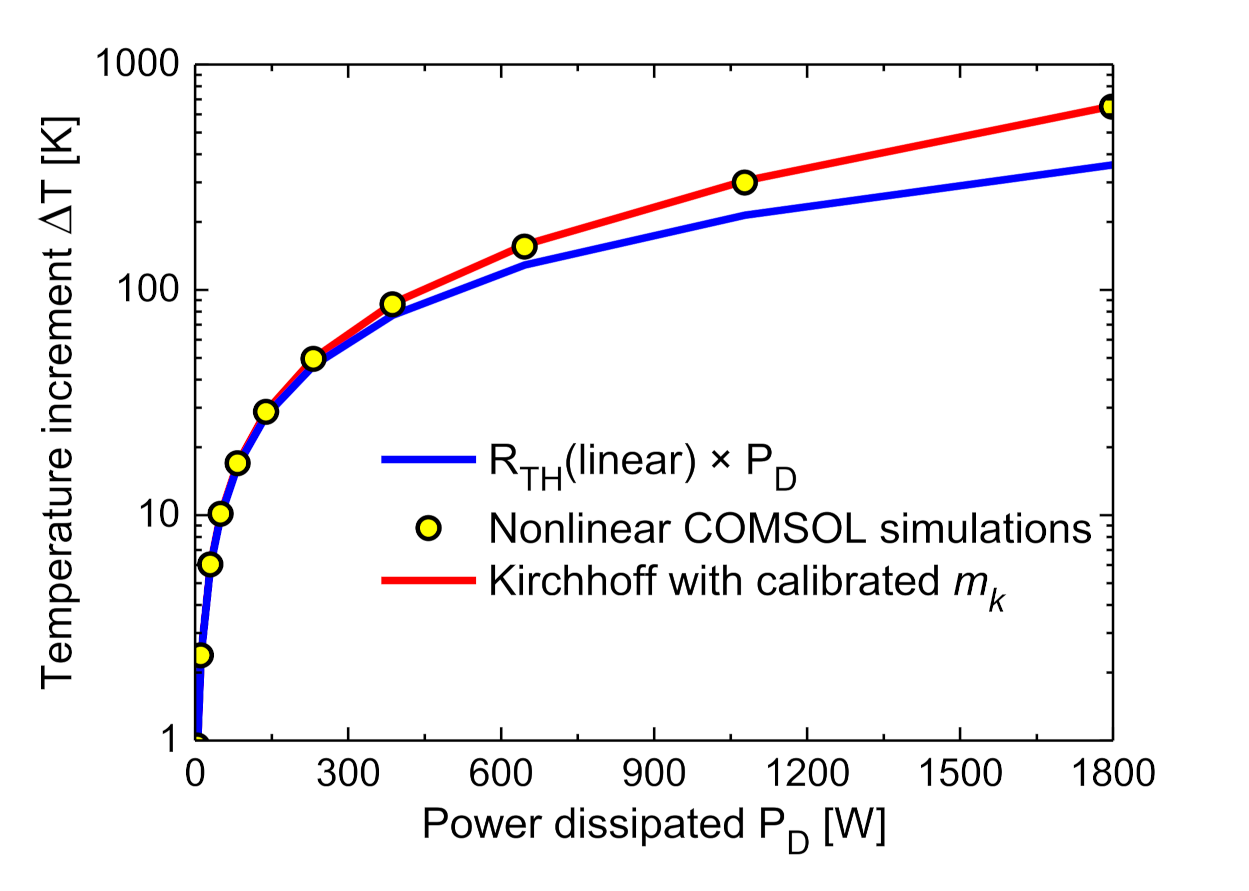
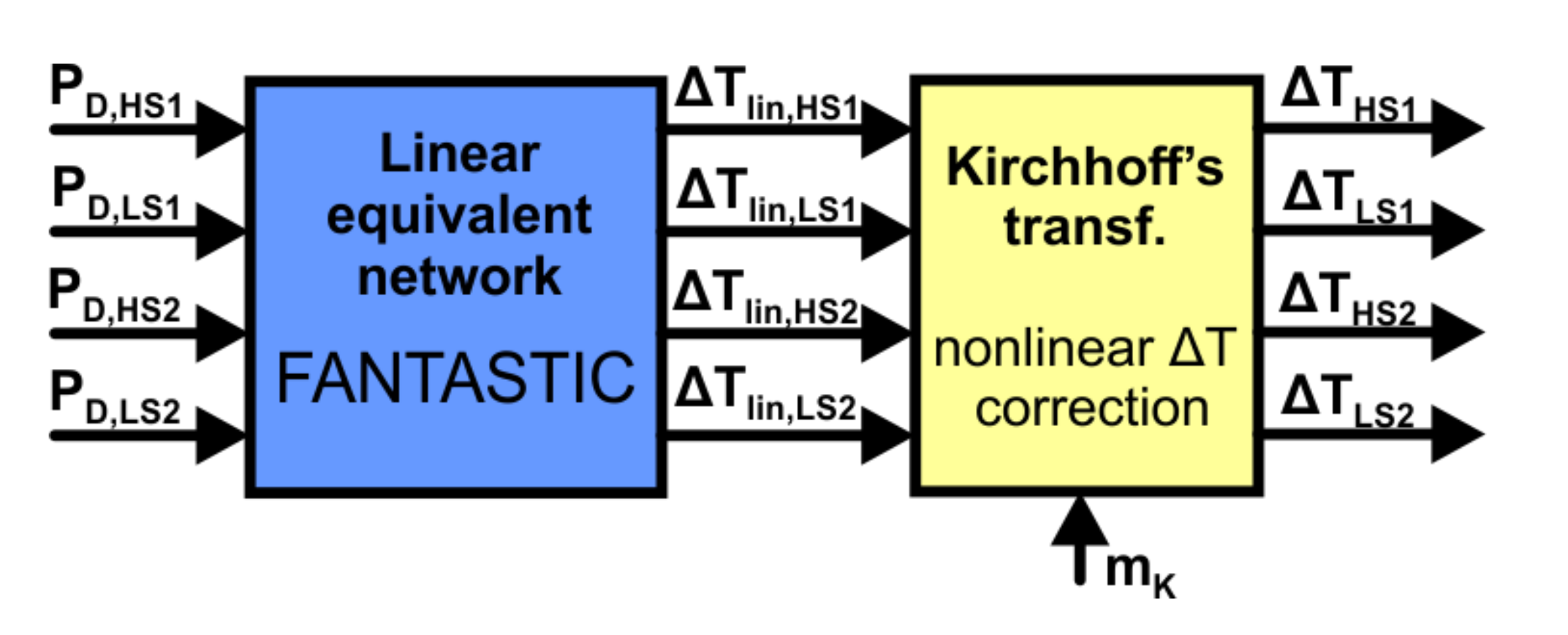
3.3. FANTASTIC-Based Thermal Modeling Including Nonlinear Effects

The power-temperature feedback is implemented by a thermal feedback block (TFB) comprising a linear equivalent network automatically extracted by FANTASTIC [32,33]. Differently from approaches based on Foster-like thermal networks [34], FANTASTIC relies on a model-order reduction technique and it does not require to perform thermal simulations in 3-D FEM software packages; it can be also adopted in multi-source thermal problems, typically making use of matrix-based approaches to account for the thermal coupling between devices [35]. It must be remarked that nonlinear thermal effects play a relevant role in typical applications of SiC devices [36]. While other techniques allow building thermal networks accounting for the temperature dependence of the thermal conductivity [37], in this work a nonlinear correction applied through the Kirchhoff’s transformation [38] was required. By exploiting the TEOL, the TFB can be employed in circuit simulators to enable the ET feedback. More specifically, the power nodes of the transistor subcircuits represent the TFB input currents, while the thermal ones are connected to its output voltages. The resulting macrocircuit (which completely describes the coupled electrical-thermal problem) can be solved by any SPICE-like program (like PSPICE, LTSPICE, Eldo, ADS, SIMetriX) in relatively short times without occurrence of convergence issues; in this work, the SIMetriX framework [39] was exploited.
The linear equivalent network extraction procedure is briefly explained in the following. First, an exceptionally detailed 3-D geometry is created from PM structural data in the finite-element method (FEM) environment of COMSOL Multiphysics [40], as shown in Figure 4; the building process is entirely automated by the in-house routine presented in [41], which relies on the livelink between COMSOL and MATLAB. Then, the domain is discretized into a tetrahedral grid; a smart meshing approach was conceived in order to make the grid finer in the surroundings of the dies (Figure 4). The mesh is in turn fed to FANTASTIC, which automatically builds a reduced-order model and extracts the corresponding equivalent network. Such a network associates the powers PD dissipated by the heat sources of the four VDMOS devices (inputs) to their temperature rises ΔTlin averaged on the channel regions located on the top surface (outputs) under linear thermal conditions.
The thermal problem was set as follows. Four heat sources (one for each device) were considered to coincide with the active region of the transistors located on the top surface of the dies. Adiabatic boundary conditions were defined on all external surfaces except for the bottom baseplate one, on which a convective heat transfer coefficient h = 3 × 10⁶ W/m2K was chosen to emulate the presence of a thermochuck (cold plate) [9]; it must be remarked that any h value can in principle be adopted to model the effect of different cooling solutions.
Nonlinear thermal effects are accounted for by means of the Kirchhoff’s transformation [34]
Δ T = T 0 [ m k + ( 1 m k ) Δ T lin + T 0 T 0 ] 1 1 m k T 0
where ΔT represents the nonlinear-corrected temperature increment and mk is a fitting parameter, strongly depending on (i) the geometry and materials of the assembly and (ii) the boundary conditions of the thermal problem. The calibration of mk was made through the following procedure. First, the self-heating thermal resistance (RTH) of an individual VDMOS transistor under linear conditions was evaluated in COMSOL as ΔTlin/PD. The temperature dependence of the thermal conductivities was then activated, and many COMSOL simulations were carried out with PD logarithmically spanning the wide 1.8–1800 W range; hence, the nonlinear temperature rise averaged on the channel region was obtained as a function of PD. As a final step, parameter mk was calibrated through a least-squares algorithm to achieve the best agreement between the temperature rises ΔT obtained through Equation (7) from ΔTlin = RTH × PD and those simulated by COMSOL under nonlinear conditions. Figure 5 shows the results of the fitting procedure, which demonstrate that the choice of the parameter mk = 0.9443 allows achieving an excellent agreement over a broad range of ΔT values (0–700 K).

4. Results

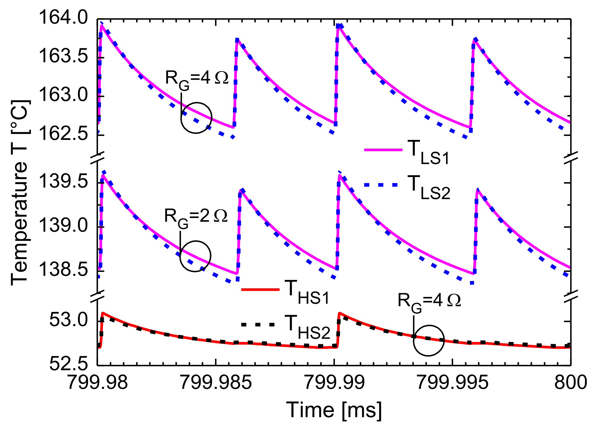
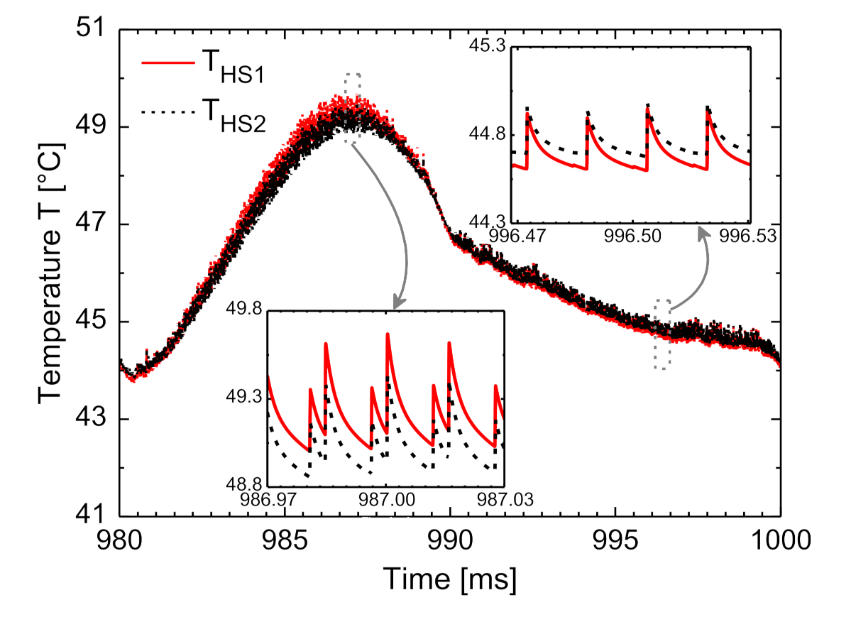
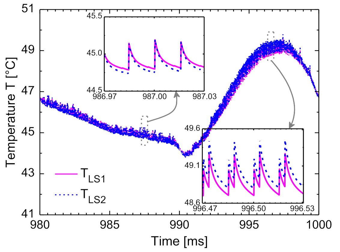
4.1. Case-Study #1: DC-DC Step-Up Converter

As a first case-study, the proposed simulation approach was applied to a 30 kW synchronous step-up DC-DC converter including the PM under analysis. Figure 6 illustrates the schematic with emphasis on device subcircuits and parasitics. The connections are designed to realize the circuit configuration with two parallel devices at the high side (HS) and two parallel devices at the low side (LS); the gate signals VG and VG’ were generated to control the LS and HS devices, respectively. A switching frequency fSW = 100 kHz was considered. A sketch of the TFB is depicted in Figure 7.
Table 2 summarizes the circuit parameters adopted in the ET simulations, chosen so as to respect the specifications on the output power. The parasitics were accounted for through the lumped elements Rσ, Lσ, and CM, the values of which at fSW = 100 kHz were obtained by elaborating the experimentally extracted total loop parasitic inductance and resistance, and common-mode capacitance shown in Table 1.
The efficiency of the step-up converter was computed to be η = 94.35% by elaborating the ET simulation results. Figure 8 shows the PD values of the four devices at the limit cycle, while their operating temperatures averaged on the channel regions are reported in Figure 9. The circuit configuration makes the LS devices dissipate much more power with respect to the HS ones, which results in a significant temperature difference between them (Figure 9). The small temperature ripple (~1%) is due to the slow thermal dynamic behavior induced by the large thermal capacitance associated with the thick Cu baseplate. After the dynamic ET simulation run, FANTASTIC, aided by a code to account for the Kirchhoff’s transformation, enables the reconstruction of the whole spatial temperature field in the PM at chosen time instants with negligible computational cost (e.g., [20]). This is a key option offered to designers, as the inspection of selected thermal maps represents a valuable support to estimate the PM reliability. Figure 10 depicts the PM temperature field extracted at t = 800 ms; an interesting finding it that the maximum temperature of the LS devices (~190 °C) is ~30 °C higher than the average one (Figure 9).
As proof of the suitability of the proposed approach in parametric analyses, additional exemplificative simulations were performed to quantify the converter performances by modifying circuit parameters. To this aim, the gate resistance RG and the switching frequency fSW were varied in the ranges 2–6 Ω and 90–105 kHz, respectively. While the RG range was chosen according to values typically adopted for SiC-based VDMOS, fSW values were selected in a narrow range to ensure the circuit working in continuous current mode given the passive components values (i.e., L1 = 5 mH and COUT = 10 µF); in principle, any value of fSW and RG can be adopted. As a figure of merit of the circuit, η was evaluated and reported in Table 3, while Figure 9 also shows the lower temperatures of the LS transistors obtained by reducing the gate resistance RG from 4 Ω down to 2 Ω.
The main findings can be summarized as follows:
  • higher RG values increase η; however, designers should also consider the detrimental effects on di/dt.
  • by reducing fSW, the losses due to the reactive components and PM parasitics are mitigated, thus leading to higher η values.
The six simulations performed for this analysis allowed offering further evidence of the excellent convergence properties and the low CPU time requirements (~2 h for a time window of 800 ms on a PC equipped by a single i7-4710HQ CPU and a 16 GB RAM).

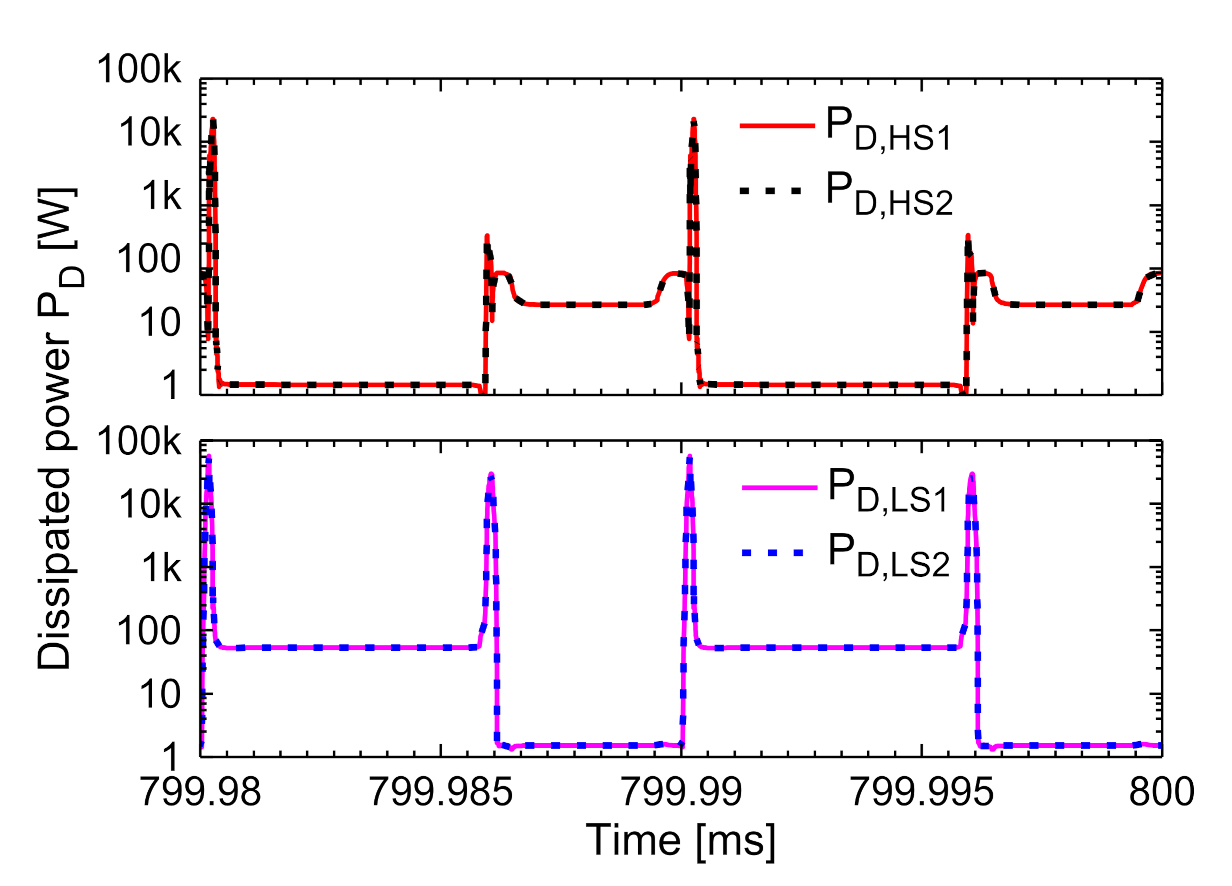
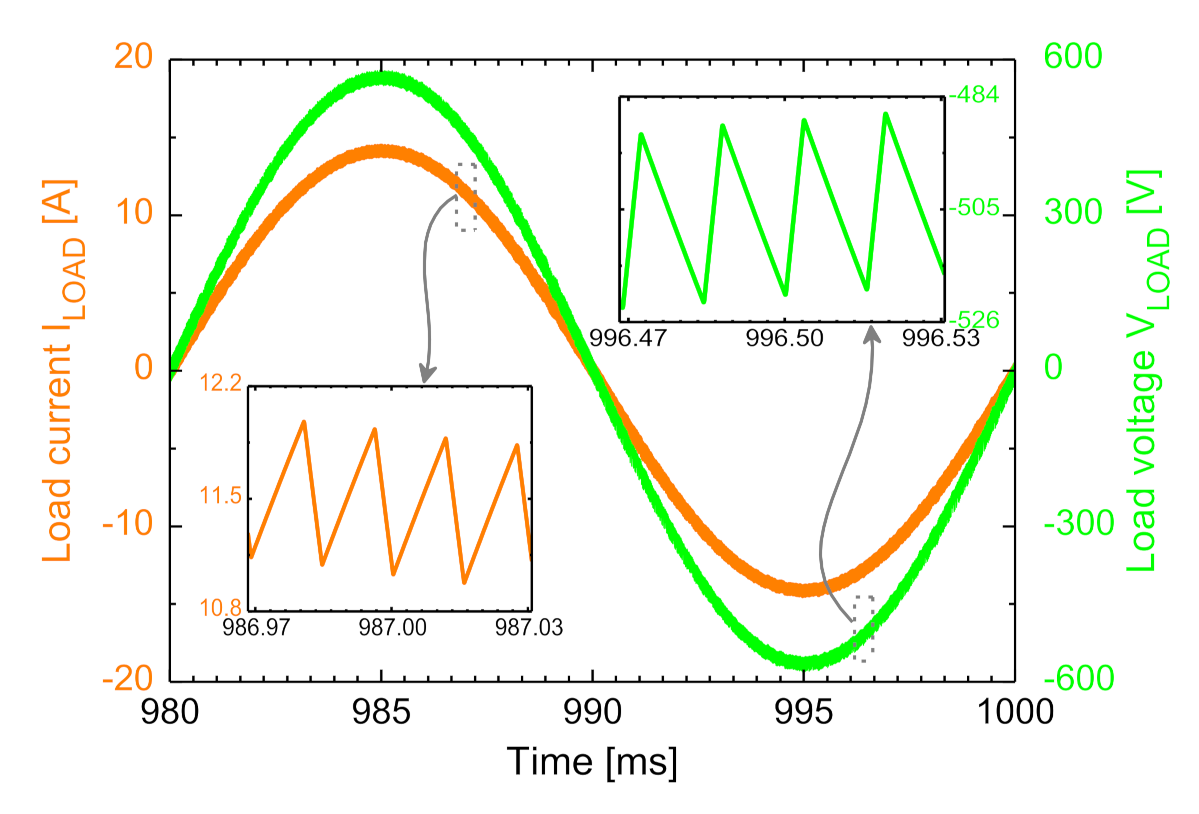
4.2. Case-Study #2: Single-Phase Inverter

ET simulations of a single-phase inverter were also performed; the approach was applied to the macrocircuit schematically depicted in Figure 11. The 50 Hz-400 V RMS inverter was designed to achieve a high efficiency value (~92%) providing a PLOAD = 4.5 kW RMS to RLOAD; such electrical rates respect European AC standards and are compatible with wind- and solar-energy conversion [42,43]. Furthermore, the circuit can be easily modified into a double-pulse tester, which is widely adopted in parametric switching characterization of transistors [44]. The circuit required the use of an inverter control unit (ICU). As the load current is detected by means of a current sensing, the ICU generates ad-hoc voltage signals (VG_LS and VG_HS) to be fed to the gate drivers of the transistors. The control is based on a duty-cycle modulation technique. While the SIMetriX macrocircuit includes the same lumped parasitic components used for the DC-DC converter simulations, their values were varied according to fSW (i.e., 64 kHz for the case study). Concerning the power-temperature feedback, the same approach shown in Section 4.1 was adopted (Figure 7). The parameters used in the inverter simulations are summarized in Table 4.
An ET simulation of 1 s required ~1 h on a standard PC. The efficiency of the inverter was evaluated to be η = 91.39%. The current and voltage waveforms on the resistive load are shown in Figure 12 over a 20 ms-wide time window at the limit cycle. The duty-cycle modulation technique leads the HS (LS) devices to dissipate more power in the first (second) half of the period. This is also confirmed by Figure 13 and Figure 14, which depict the average temperature of the HS and LS devices, respectively. It must be underlined that (i) the high efficiency, (ii) the good boundary conditions applied to the bottom of the Cu baseplate, and (iii) the high RLOAD value contribute to achieve low temperature increments (~30 °C) with respect to T0. As a main difference with the DC-DC converter, in which the LS devices turned out to be hotter than the HS ones, here the device temperatures are more evenly distributed. Again, the post-processing feature of FANTASTIC was exploited to extract the nonlinear-corrected temperature maps on the PM at the time instants t = 987.0 ms (Figure 15a) and t = 996.5 ms (Figure 15b).
As a last analysis, a parametric investigation (similar to the one carried out on the DC-DC converter) was conducted on the single-phase inverter. Table 5 shows the inverter efficiency η as a function of fSW and RG. The influence of such parameters was evaluated in a fast, yet trustworthy, simulation session that lasted ~4 h and proved the suitability of the approach even in parametric analyses of AC circuits.

5. Conclusions

An efficient and versatile strategy for fast and accurate dynamic electrothermal simulations has been applied to a state-of-the-art multichip power module including four 3.3 kV SiC VDMOS transistors arranged in a half-bridge configuration. The approach relies on a fully circuital representation of the whole module based on the thermal equivalent of the Ohm’s law. The individual devices are described with subcircuits implementing a behavioral model, the temperature-sensitive parameters of which are allowed to vary during the simulation run. The power-temperature feedback is included with an equivalent thermal network automatically extracted by FANTASTIC with an advanced model-order reduction technique applied to a 3-D COMSOL mesh representing a very accurate replica of the real module; such a network is in turn equipped with a numerically calibrated Kirchhoff’s transformation to account for nonlinear thermal effects.
The strategy has been exploited to simulate a synchronous step-up DC-DC converter and a single-phase inverter embedding the aforementioned power module. In both cases, circuit parasitics have been included, the values of which were calibrated on the basis of the total loop parasitic resistance/inductance and common-mode parasitic capacitance experimentally extracted in a preliminary stage. The SIMetriX software has been selected to perform electrothermal simulations of the converter and inverter macrocircuits, although any other SPICE-like circuit software packages could in principle be used. Despite the complexity of the problem, the high switching frequency, the high temperatures reached, and the long-time range analyzed, the simulations have been carried out in a relatively short time on a standard PC without convergence issues; more specifically, 1 h and 2 h were required to perform the 800 ms-long DC-DC converter and 1 s-long AC inverter ET simulations, respectively. This allowed for effortlessly conducting an illustrative study on the impact of key parameters on the circuits performance (i.e., in terms of efficiency). The analysis has shown that the proposed approach can be fruitfully used for the analysis and design of power conversion architectures in strategic domains of societal infrastructure, such as railway traction and renewable energy conversion.

Author Contributions

Conceptualization, C.S., A.P.C., M.R., V.d., L.C., A.C., G.B., and A.I.; methodology, L.C., A.B., R.N.T., A.C., G.B., and A.I.; validation, A.B.; formal analysis, M.R., L.C., and R.N.T.; investigation, C.S., A.P.C., and V.d.; resources, C.S., A.P.C., V.d., A.C., G.B., and A.I.; data curation, C.S., A.P.C., and M.R.; writing—original draft preparation, C.S., A.P.C., and V.d.; writing—review and editing, C.S., A.P.C., V.d., and A.B.; supervision, C.S., A.P.C., V.d., A.C., G.B., and A.I. All authors have read and agreed to the published version of the manuscript.

Funding

This research received no external funding.

Acknowledgments

The funding for the Ph.D. activity of Ciro Scognamillo was generously donated by the Rinaldi family in the memory of Niccolò Rinaldi, a bright Professor and Researcher of University of Naples Federico II, prematurely passed away in 2018.

Conflicts of Interest

The authors declare no conflict of interest.

References

  1. Dusmezand, S.; Khaligh, A. A charge-nonlinear-carrier-controlled reduced-part single-stage integrated power electronics interface for automotive applications. IEEE Trans. Veh. Technol. 2013, 63, 1091–1103. [Google Scholar] [CrossRef]
  2. Gu, C.; Yan, H.; Yang, J.; Sala, G.; De Gaetano, D.; Wang, X.; Galassini, A.; Degano, M.; Zhang, X.; Buticchi, G. A multiport power conversion system for the more electric aircraft. IEEE Trans. Transp. Electrif. 2020, 6, 1707–1720. [Google Scholar] [CrossRef]
  3. Abbasi, M.; Lam, J. A SiC-driven modular step-up converter with soft-switched module having 1:1 turns ratio multiphase transformer for wind systems. IEEE Trans. Ind. Electron. 2019, 66, 7055–7066. [Google Scholar] [CrossRef]
  4. Bindra, A. Wide-Bandgap-Based Power Devices: Reshaping the power electronics landscape. IEEE Power Electron. Mag. 2015, 2, 42–47. [Google Scholar] [CrossRef]
  5. Millán, J.; Godignon, P.; Perpiñà, X.; Pérez-Tomás, A.; Rebollo, J. A Survey of Wide Bandgap Power Semiconductor Devices. IEEE Trans. Power Electron. 2014, 29, 2155–2163. [Google Scholar] [CrossRef]
  6. Okumura, H. A roadmap for future wide bandgap semiconductor power electronics. MRS Bull. 2015, 40, 439–444. [Google Scholar] [CrossRef]
  7. Hussein, A.; Mouawad, B.; Castellazzi, A. Dynamic performance analysis of a 3.3 kV SiC MOSFET half-bridge module with parallel chips and body-diode freewheeling. In Proceedings of the 2018 IEEE 30th International Symposium on Power Semiconductor Devices and ICs (ISPSD), Chicago, IL, USA, 13–17 May 2018. [Google Scholar]
  8. Catalano, A.P.; Trani, R.; Scognamillo, C.; d’Alessandro, V.; Castellazzi, A. Optimization of thermal vias design in PCB-based power circuits. In Proceedings of the 2020 21st International Conference on Thermal, Mechanical and Multi-Physics Simulation and Experiments in Microelectronics and Microsystems (EuroSimE), Cracow, Poland, 5–8 July 2020. [Google Scholar]
  9. Catalano, A.P.; Scognamillo, C.; d’Alessandro, V.; Castellazzi, A. Numerical simulation and analytical modeling of the thermal behavior of single-and double-sided cooled power modules. IEEE Trans. Compon. Packag. Manuf. Technol. 2020, 10, 1446–1453. [Google Scholar] [CrossRef]
  10. Martin, C.; Schanen, J.L.; Guichon, J.M.; Pasterczyk, R. Analysis of electromagnetic coupling and current distribution inside a power module. IEEE Trans. Ind. Appl. 2007, 43, 893–901. [Google Scholar] [CrossRef]
  11. Bryant, A.; Parker-Allotey, N.A.; Hamilton, D.; Swan, I.; Mawby, P.A.; Ueta, T.; Nishijima, T.; Hamada, K. A Fast Loss and Temperature Simulation Method for Power Converters, Part I: Electrothermal Modeling and Validation. IEEE Trans. Power Electron. 2012, 27, 248–257. [Google Scholar] [CrossRef]
  12. Van Petegem, W.; Geeraertsk, B.; Sansen, W.; Graindourze, B. Electrothermal simulation and design of integrated circuits. IEEE J. Solid-State Circ. 1994, 29, 143–146. [Google Scholar] [CrossRef]
  13. Wünsche, S.; Clauß, C.; Schwarz, P.; Winkler, F. Electro-thermal circuit simulation using simulator coupling. IEEE Trans. Very Large Scale Integr. (VLSI) Syst. 1997, 5, 277–282. [Google Scholar] [CrossRef] [Green Version]
  14. Chvála, A.; Donoval, D.; Marek, J.; Príbytný, P.; Molnár, M.; Mikolášek, M. Fast 3-D electrothermal device/circuit simulation of power superjunction MOSFET based on SDevice and HSPICE interaction. IEEE Trans. Electron Devices 2014, 61, 1116–1122. [Google Scholar] [CrossRef]
  15. Breglio, G.; Irace, A.; Napoli, E.; Riccio, M.; Spirito, P. Experimental detection and numerical validation of different failure mechanisms in IGBTs during unclamped inductive switching. IEEE Trans. Electron Devices 2012, 60, 563–570. [Google Scholar] [CrossRef]
  16. Arvanitopoulos, A.; Lophitis, N.; Gyftakis, K.N.; Perkins, S.; Antoniou, M. Validated physical models and parameters of bulk 3C–SiC aiming for credible technology computer aided design (TCAD) simulation. Semicond. Sci. Technol. 2017, 32, 104009. [Google Scholar] [CrossRef] [Green Version]
  17. Romano, G.; Fayyaz, A.; Riccio, M.; Maresca, L.; Breglio, G.; Castellazzi, A.; Irace, A. A comprehensive study of short-circuit ruggedness of silicon carbide power MOSFETs. IEEE J. Emerg. Sel. Top. Power Electron. 2016, 4, 978–987. [Google Scholar]
  18. Catalano, A.P.; Riccio, M.; Codecasa, L.; Magnani, A.; Romano, G.; d’Alessandro, V.; Maresca, L.; Rinaldi, N.; Breglio, G.; Irace, A. Model-order reduction procedure for fast dynamic electrothermal simulation of power converters. Lect. Notes Electr. Eng. 2019, 512, 81–87. [Google Scholar]
  19. d’Alessandro, V.; Catalano, A.P.; Scognamillo, C.; Codecasa, L.; Zampardi, P.J. Analysis of electrothermal effects in devices and arrays in InGaP/GaAs HBT technology. Electronics 2021, 10, 757. [Google Scholar] [CrossRef]
  20. d’Alessandro, V.; Codecasa, L.; Catalano, A.P.; Scognamillo, C. Circuit-based electrothermal simulation of multicellular SiC power MOSFETs using FANTASTIC. Energies 2020, 13, 4563. [Google Scholar] [CrossRef]
  21. Scognamillo, C.; Catalano, A.P.; Borghese, A.; Tripathi, R.N.; Riccio, M.; d’Alessandro, V.; Codecasa, L.; Castellazzi, A.; Breglio, G.; Irace, A. Electrothermal modeling, simulation, and electromagnetic characterization of a 3.3 kV SiC MOSFET power module. In Proceedings of the 33rd International Symposium on Power Semiconductor Devices and ICs (ISPSD), Nagoya, Japan, 30 May–3 June 2021. [Google Scholar]
  22. Castellazzi, A.; Fayyaz, A.; Gurpinar, E.; Hussein, A.; Li, J.; Mouawad, B. Multi-Chip SiC MOSFET Power Modules for Standard Manufacturing, Mounting and Cooling. In Proceedings of the International Power Electronics Conference (IPEC-Niigata 2018-ECCE Asia), Niigata, Japan, 20–24 May 2018. [Google Scholar]
  23. Scognamillo, C.; Catalano, A.P.; Castellazzi, A.; d’Alessandro, V. Numerical analysis of the thermal impact of ceramic materials in double-sided cooled power modules. In Proceedings of the IEEE International Workshop on Thermal Investigations of ICs and Systems (THERMINIC), Berlin, Germany, 14 September–9 October 2020. [Google Scholar]
  24. Scognamillo, C.; Catalano, A.P.; Lasserre, P.; Duchesne, C.; d’Alessandro, V.; Castellazzi, A. Combined experimental-FEM investigation of electrical ruggedness in double-sided cooled power modules. Microelectron. Reliab. 2020, 114, 113742. [Google Scholar] [CrossRef]
  25. Scognamillo, C.; Catalano, A.P.; Trani, R.; d’Alessandro, V.; Castellazzi, A. 3-D FEM investigation on electrical ruggedness of double-sided cooled power modules. In Proceedings of the 21st International Conference on Thermal, Mechanical and Multi-Physics Simulation and Experiments in Microelectronics and Microsystems (EuroSimE), Cracow, Poland, 5–8 July 2020. [Google Scholar]
  26. Available online: https://www.hioki.com/en/products/detail/?product_key=5539 (accessed on 10 April 2021).
  27. d’Alessandro, V.; Magnani, A.; Riccio, M.; Breglio, G.; Irace, A.; Rinaldi, N.; Castellazzi, A. SPICE modeling and dynamic electrothermal simulation of SiC power MOSFETs. In Proceedings of the IEEE International Symposium on Power Semiconductor Devices & IC’s (ISPSD), Waikoloa, HI, USA, 15–19 June 2014. [Google Scholar]
  28. Riccio, M.; d’Alessandro, V.; Romano, G.; Maresca, L.; Breglio, G.; Irace, I. A temperature-dependent SPICE model of SiC power MOSFETs for within and out-of-SOA simulations. IEEE Trans. Power Electron. 2018, 99, 8020–8029. [Google Scholar] [CrossRef]
  29. ON Semiconductor. Physically Based, Scalable SPICE Modeling Methodologies for Modern Power Electronic Devices. TND6260/DRev. 2021, 2. Available online: https://zbook.org/read/c9dec_tnd6260-physically-based-scalable-spice-modeling.html (accessed on 30 July 2021).
  30. Borghese, A.; Riccio, M.; Fayyaz, A.; Castellazzi, A.; Maresca, L.; Breglio, G.; Irace, A. Statistical analysis of the electrothermal imbalances of mismatched parallel SiC power MOSFETs. IEEE J. Emerg. Sel. Top. Power Electron. 2019, 7, 1527–1538. [Google Scholar] [CrossRef]
  31. Zarebski, J.; Gorecki, K. Modelling TrenchMOSFETs in SPICE. In Proceedings of the IEEE International Conference on Electronics, Circuits and Systems, Saint Julian’s, Malta, 31 August–3 September 2008; pp. 73–76. [Google Scholar]
  32. Codecasa, L.; d’Alessandro, V.; Magnani, A.; Rinaldi, N.; Zampardi, P.J. FAst Novel Thermal Analysis Simulation Tool for Integrated Circuits (FANTASTIC). In Proceedings of the International Workshop on Thermal Investigations of ICs and Systems (THERMINIC), Greenwich, UK, 24–26 September 2014. [Google Scholar]
  33. Magnani, A.; d’Alessandro, V.; Codecasa, L.; Zampardi, P.J.; Moser, B.; Rinaldi, N. Analysis of the influence of layout and technology parameters on the thermal impedance of GaAs HBT/BiFET using a highly-efficient tool. In Proceedings of the IEEE Compound Semiconductor Integrated Circuit Symposium (CSICS), La Jolla, CA, USA, 19–22 October 2014. [Google Scholar]
  34. Górecki, K.; Gòrecki, P.; Zarębski, J. Measurements of Parameters of the Thermal Model of the IGBT Module. IEEE Trans. Instrum. Meas. 2019, 68, 4864–4875. [Google Scholar] [CrossRef]
  35. Schweitzer, D. Thermal transient characterization of semiconductor devices with multiple heat sources—Fundamentals for a new thermal standard. In Proceedings of the IEEE International Workshop on Thermal Investigations of ICs and Systems (THERMINIC), Berlin, Germany, 25–27 September 2013; pp. 301–304. [Google Scholar]
  36. Codecasa, L.; d’Alessandro, V.; Magnani, A.; Irace, A. Circuit-based electrothermal simulation of power devices by an ultrafast nonlinear MOR approach. IEEE Trans. Power Electron. 2016, 31, 5906–5916. [Google Scholar] [CrossRef]
  37. Górecki, K.; Górecki, P. Nonlinear Compact Thermal Model of the IGBT Dedicated to SPICE. IEEE Trans. Power Electron. 2020, 35, 13420–13428. [Google Scholar] [CrossRef]
  38. Poulton, K.; Knudsen, K.L.; Corcoran, J.J.; Wang, K.C.; Pierson, R.L.; Nubling, R.B.; Chang, M.C.F. Thermal design and simulation of bipolar integrated circuits. IEEE J. Solid-State Circ. 1992, 27, 1378–1387. [Google Scholar] [CrossRef]
  39. SIMetrix User’s Manual 13/5/10; SIMetrix Technologies Ltd.: Thatcham, UK, 1992–2010.
  40. COMSOL Multiphysics, User’s Guide, Release 5.3A; COMSOL Inc.: Burlington, MA, USA, 2018.
  41. d’Alessandro, V.; Catalano, A.P.; Codecasa, L.; Zampardi, P.J.; Moser, B. Accurate and efficient analysis of the upward heat flow in InGaP/GaAs HBTs through an automated FEM-based tool and Design of Experiments. Int. J. Numer. Modeling Electron. Netw. Devices Fields 2019, 32, e2530. [Google Scholar] [CrossRef]
  42. Kojabadi, H.M.; Chang, L.; Boutot, T. Development of a novel wind turbine simulator for wind energy conversion systems using an inverter-controlled induction motor. IEEE Trans. Energy Convers. 2004, 19, 547–552. [Google Scholar] [CrossRef]
  43. Dogga, R.; Pathak, M.K. Recent trends in solar PV inverter topologies. Solar Energy 2019, 183, 57–73. [Google Scholar] [CrossRef]
  44. Mouawad, B.; Hussein, A.; Castellazzi, A. A 3.3 kV SiC MOSFET half-bridge power module. In Proceedings of the 10th International Conference on Integrated Power Electronics Systems, Stuttgart, Germany, 20–22 March 2018. [Google Scholar]
Figure 1. Picture of the state-of-the-art PM under investigation: it embeds four 3.3 kV SiC VDMOS transistors placed on two separate DBC substrates, which in turn lie on a 120 × 60 mm2 Cu baseplate.
Energies 14 04683 g001
Figure 2. Schematic cross-section (not to scale) of the PM under investigation. The materials are identified by different colors. Evidenced are the Al wire bonds, the Cu baseplate, and the DBC substrate comprising Cu metallization and AlN layer.
Energies 14 04683 g002
Figure 3. SPICE-compatible schematic implementing the behavioral model of the 3.3 kV SiC VDMOS transistor under analysis. The model includes three active components (the MOSFET, simply denoted as MOS, JRJFET, and DBODY) and two nonlinear resistors (REPI and RBODY).
Energies 14 04683 g003
Figure 4. 3-D view of the PM geometry (left to the red dashed line) and tetrahedral mesh (right) automatically constructed in the COMSOL environment (the insulating gel is set as transparent for illustrative purposes). An exact replica of the real structure (Figure 1) was obtained.
Energies 14 04683 g004
Figure 5. Temperature increments vs. power PD dissipated by the heat source. Comparison between nonlinear FEM simulations (yellow dots) and values obtained with the calibrated Kirchhoff’s transformation (red curve). The graph also reports ΔTlin given by the product of the linear thermal resistance value (RTH) and PD (blue curve).
Energies 14 04683 g005
Figure 6. Schematic of the half-bridge circuit driven in a synchronous step-up configuration. The light green boxes are the transistor subcircuits depicted in Figure 3, while the parasitics are modeled with the passive components drawn in red.
Energies 14 04683 g006
Figure 7. Sketch of the TFB comprising (i) the linear equivalent network automatically built by FANTASTIC (light blue box) and (ii) the nonlinear correction performed by the preliminarily tuned Kirchhoff’s transformation (light yellow).
Energies 14 04683 g007
Figure 8. SIMetriX simulation of the macrocircuit representing the DC-DC converter: power dissipated by the four VDMOS transistors vs. time in a two-period-long window at the limit cycle; the top (bottom) curves show the values referred to HS (LS) devices.
Energies 14 04683 g008
Figure 9. SIMetriX simulation of the macrocircuit representing the DC-DC converter: temperature of the four VDMOS transistors (averaged on the active area) vs. time in a two-period-long window at the limit cycle. Also reported is the temperature evolution of the LS devices obtained by reducing the gate resistance RG from 4 Ω (default value) down to 2 Ω.
Energies 14 04683 g009
Figure 10. Nonlinear-corrected spatial temperature distribution in the PM extracted by FANTASTIC in a post-processing stage, corresponding to the time instant t = 800.0 ms of the DC-DC converter simulation. The insulating gel is set as transparent for illustrative purposes. The location of LS and HS devices is also highlighted.
Energies 14 04683 g010
Figure 11. Schematic of the half-bridge circuit driven in a single-phase inverter configuration. Evidenced are the experimentally-extracted parasitics (red), the output current and voltage (orange and green arrow, respectively), the VDMOS subcircuits described in Figure 3 (light green boxes), the current sensing component (orange), the ICU (turquoise), and the logic signals (grey dashed lines) fed to the gate drivers of the four transistors.
Energies 14 04683 g011
Figure 12. Simulated ILOAD (orange curve) and VLOAD (green) vs. time in the last 20 ms window. Magnifications highlighting the ripple of ILOAD and VLOAD in four-period-long windows are also reported on the bottom-left and top-right corners, respectively.
Energies 14 04683 g012
Figure 13. Simulated temperature of the HS devices vs. time in the last 20 ms window. Magnifications highlighting the temperature ripple in four-period-long windows are also reported on the bottom-left and top-right corners.
Energies 14 04683 g013
Figure 14. Simulated temperature of the LS devices vs. time in the last 20 ms window. Magnifications highlighting the temperature ripple in four-period-long windows are also reported on the top-left and bottom-right corners.
Energies 14 04683 g014
Figure 15. Nonlinear corrected spatial temperature distributions extracted by FANTASTIC in a post-processing stage. The maps correspond to the time instants (a) t = 987.0 ms and (b) 996.5 ms of the inverter simulation. The insulating gel is set as transparent for illustrative purposes. The location of LS and HS devices is also highlighted.
Energies 14 04683 g015
Table 1. Values of the experimentally extracted parasitics at the frequencies of interest.
fSW = 32 kHzfSW = 64 kHzfSW = 100 kHz
Total loop parasitic resistance~5.4 mΩ~5.2 mΩ~4 mΩ
Total loop parasitic inductance~130 nH~30 nH~120 nH
Common-mode capacitance~121 pF~118 pF~118 pF
Table 2. Values of the DC-DC converter circuit parameters adopted in SIMetriX.
ParameterValue
VIN800 V
Rgen0.1 Ω
L15 mH
RL10.1 Ω
POUT29 kW
RG4 Ω
COUT10 µF
ROUT120 Ω
Lσ30 nH
Rσ4 mΩ
LWB1 nH
CM118 pF
fSW100 kHz
TON5.5 µs
Table 3. Outcome of the parametric analysis conducted on the DC-DC converter: the efficiency (η) evaluated at different RG and fSW values.
RG2 Ω4 Ω6 Ω
η95.17%94.35%93.55%
fSW105 kHz100 kHz90 kHz
η93.49%94.35%95.59%
Table 4. Values of the inverter parameters adopted in SIMetriX.
ParameterValue
VDC1800 V
LLOAD5.8 mH
RLOAD40 Ω
POUT,RMS4.5 kW
RG2 Ω
Lσ7.5 nH
Rσ5.2 mΩ
LWB1 nH
CM118 pF
fSW64 kHz
Table 5. Outcome of the parametric analysis conducted on the inverter: efficiency (η) evaluated at different RG and fSW values.
ηRG = 2 ΩRG = 4.7 Ω
fSW = 32 kHz95.32%92.88%
fSW = 64 kHz91.39%87.32%
Publisher’s Note: MDPI stays neutral with regard to jurisdictional claims in published maps and institutional affiliations.

