Article

Implementation of an FPGA-Based Current Control and SVPWM ASIC with Asymmetric Five-Segment Switching Scheme for AC Motor Drives

Department of Electrical Engineering, Minghsin University of Science and Technology, No. 1, Xinxing Rd., Xinfeng, Hsinchu 30401, Taiwan
*
Author to whom correspondence should be addressed.
Submission received: 1 February 2021 / Revised: 25 February 2021 / Accepted: 27 February 2021 / Published: 7 March 2021
(This article belongs to the Special Issue Design and Control of Electrical Motor Drives)

Abstract

:
This paper presents the design and implementation of an application-specific integrated circuit (ASIC) for a discrete-time current control and space-vector pulse-width modulation (SVPWM) with asymmetric five-segment switching scheme for AC motor drives. As compared to a conventional three-phase symmetric seven-segment switching SVPWM scheme, the proposed method involves five-segment two-phase switching in each switching period, so the inverter switching times and power loss can be reduced by 33%. In addition, the produced PWM signal is asymmetric with respect to the center-symmetric triangular carrier wave, and the voltage command signal from the discrete-time current control output can be given in each half period of the PWM switching time interval, hence increasing the system bandwidth and allowing the motor drive system with better dynamic response. For the verification of the proposed SVPWM modulation scheme, the current control function in the stationary reference frame is also included in the design of the ASIC. The design is firstly verified by using PSIM simulation tool. Then, a DE0-nano field programmable gate array (FPGA) control board is employed to drive a 300W permanent-magnet synchronous motor (PMSM) for the experimental verification of the ASIC.

1. Introduction

The AC motor drives, including induction motors (IM), permanent-magnet synchronous motor (PMSM) drives, synchronous reluctance motors (SynRM), and others, have been very popular, being applied to electric vehicles, railway traction engines, and industrial applications such as CNC tools and robots, because they have higher power density and efficiency as compared to DC motor drives [1,2,3,4]. Since the AC motor is a time-varying, multi-variable, and nonlinear control system with very complicated dynamic characteristics, it can be reduced to a simpler linear control system by using the field-oriented vector control method [5,6,7,8,9,10,11]. In vector-controlled AC motor drives, various pulse-width modulation (PWM) techniques exist to determine the inverter switch-on and switch-off instants from the control output modulating signals. Popular examples include sinusoidal PWM (SPWM), hysteresis PWM, and space-vector PWM (SVPWM). Among them, the SPWM method generates the inverter switching signals by comparing the modulating signals with a common triangular carrier wave, in which the intersection points determine the switching points of the inverter power devices [12,13]. The hysteresis PWM method controls the inverter output currents to track the reference inputs within the hysteresis band, but with various switching frequencies [14,15]. The SVPWM method is based on the concept of voltage vector space, which can be divided into six sectors, and calculates the switch dwelling or firing time in each sector to generate the PWM signals [16,17,18,19,20,21,22,23,24,25,26,27,28,29,30,31,32,33,34,35,36,37,38,39,40]. The relationship between SVPWM and SPWM was presented in [18], which indicated that the SVPWM can be viewed as a particular form of asymmetric regular-sampled PWM. In [24], the relationship between SVPWM and three-phase SPWM was also analyzed and the implementation of them in a closed-loop feedback converter was discussed as well. The SVPWM technique is the preferred approach in most applications due to the higher voltage utilization and lower harmonic distortion (THD) than the other two methods, and hence it can extend the linear range of the vector-controlled AC motor drives. Furthermore, sensorless and direct torque control (DTC) cooperating with an SVPWM scheme for a flux-modulated permanent-magnet wheel motor and induction motor has been described owing to several advantages, such as low torque/flux ripples in motor drive and reduced direct axis current, over the conventional hysteresis direct torque control method when the motor is operated at a light or a sudden increased load [34,37,38,39,40]. The SVPWM scheme has also been extensively applied to the control of a five-phase permanent-magnet motor and multilevel inverters [35,36].
Different SVPWM techniques can be used for three-phase inverters according to the choice of the null vector on the voltage space and the number of samplings during a PWM switching period. They can be divided into seven-segment, five-segment, and three-segment techniques for the switching sequences and the choice of null vector, and classified into symmetric and asymmetric techniques according to the number of samplings during a PWM switching period as well. For the symmetric technique, the sampling period is equal to the switching period, while the sampling period is one half of the switching period for the asymmetric technique. So, the asymmetric methods have only 50% switching action in each switching period as compared with symmetric methods, and hence the sampling frequency of the current control can be doubled at a certain switching frequency. In [28], three SVPWM strategies, including symmetric seven-segment technique, symmetric five-segment technique, and asymmetric three-segment technique, were compared through simulation analysis. The switching loss of the three-segment scheme is the lowest and the seven-segment scheme performs better in terms of the THD of the output line voltage.
Figure 1 shows the rotor flux-oriented control (RFOC) structure of a PMSM motor drive with a SVPWM modulation scheme, in which an asymmetric five-segment switching is proposed rather than the conventional symmetric seven-segment switching so as to double the sampling frequency and reduce the switching loss. This control structure, from the inner to the outer loops, includes the SVPWM modulation, current control loop, torque and flux control loops, and speed control loop. Conventionally, the execution of all the control tasks is performed by using a high-performance microprocessor or dual digital signal processor (DSP) [21,41,42]. It may take a lot of computation time for the microprocessor or DSP because all the computation of the tasks is very complicated. If the computation of the current control and the SVPWM tasks can be executed by a field programmable gate array (FPGA) device, the computation load can be greatly reduced [16,17,22,25,30]. In such cases, the microprocessor or DSP can have enough time to process higher level tasks, such as position control, motion control, adaptive, fuzzy, or neural-network learning and intelligent control [43]. In [17], an eight-bit SVPWM control IC was realized with a symmetrical five-segment switching scheme, but without current control function included in the chip. In [22], a microcoded machine with a 16-bit computational ALU unit and control sequencer was designed in an FPGA for the execution of the current control and SVPWM modulation of an induction motor with symmetrical seven-segment switching scheme. However, the microcoded machine structure is very complicated.
This paper describes the design and implementation of an application-specific integrated circuit (ASIC) for a discrete-time current control and space-vector pulse-width modulation (SVPWM) with asymmetric five-segment switching scheme AC motor drives. It can not only reduce the computation load of a microprocessor or DSP, but also reduce the power transistor switching loss of the inverter. Traditionally, the current control loop is performed in the synchronously d-q rotating reference frame [3,4,5,6,7]. However, as indicated in Figure 1, the presented current control loop is performed in the stationary reference frame rather than the synchronously rotating reference frame in order to simplify the computation complexity in the FPGA device. Furthermore, because the current reference commands can be updated two times during one switching period, the current control system can also increase the sampling frequency two times so as to increase the bandwidth.
The algorithm of the proposed current control and asymmetric five-segment switching SVPWM scheme was firstly verified by using PSIM simulation tool as applied to the current control of a PMSM AC motor. The proposed SVPWM scheme and the current controller function were implemented on a DE0-nano control board with Altera Cyclone IV E FPGA device for the experimental verification.
This paper is organized as follows. The principle of the asymmetric five-segment switching SVPWM modulation scheme is described in Section 2. The simulation verification in PSIM simulation tool is analyzed in Section 3 and the FPGA implementation and the experimental results are presented in Section 4. A discussion is then given in Section 5. Finally, the conclusion is given in Section 6.

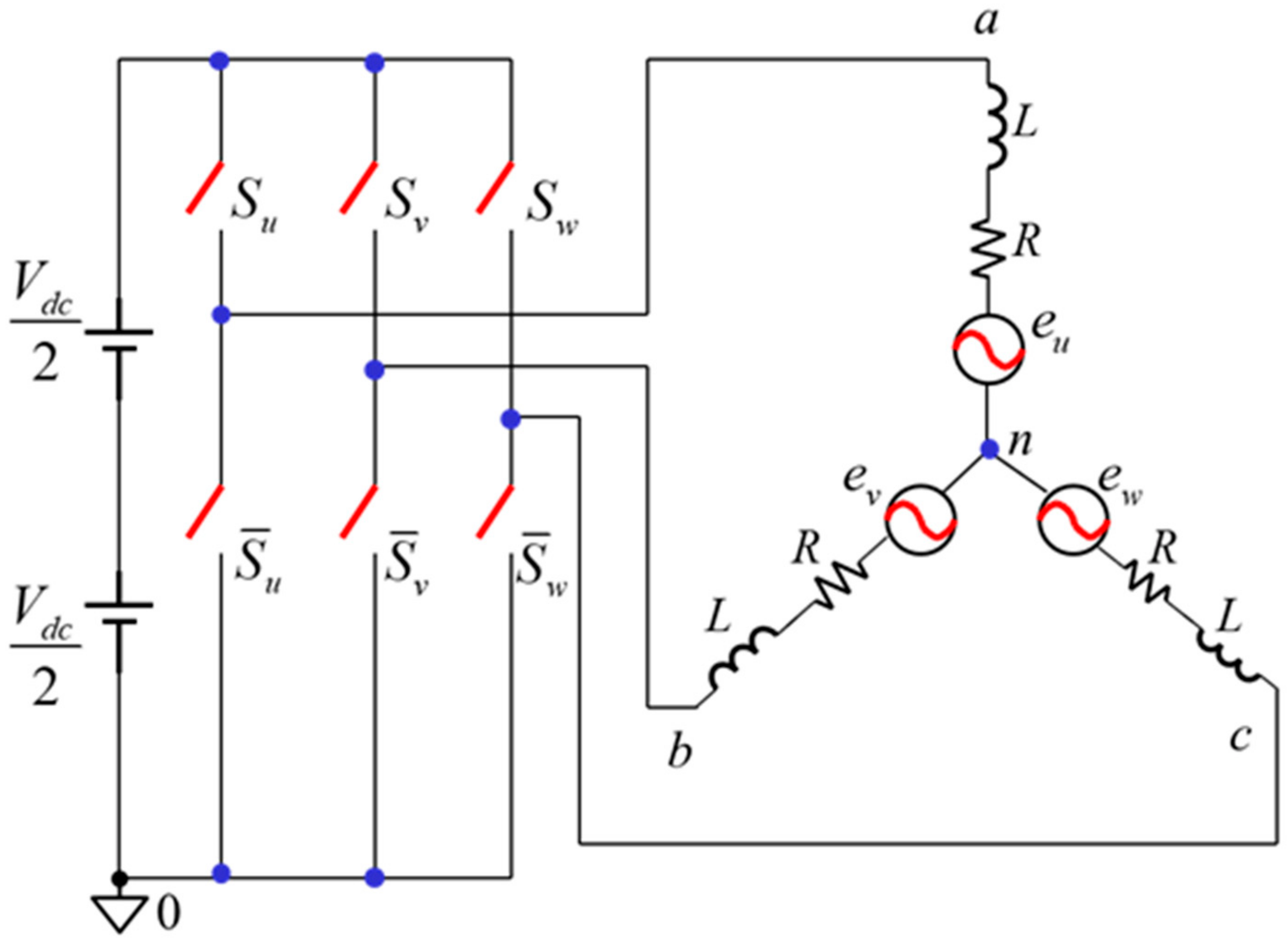
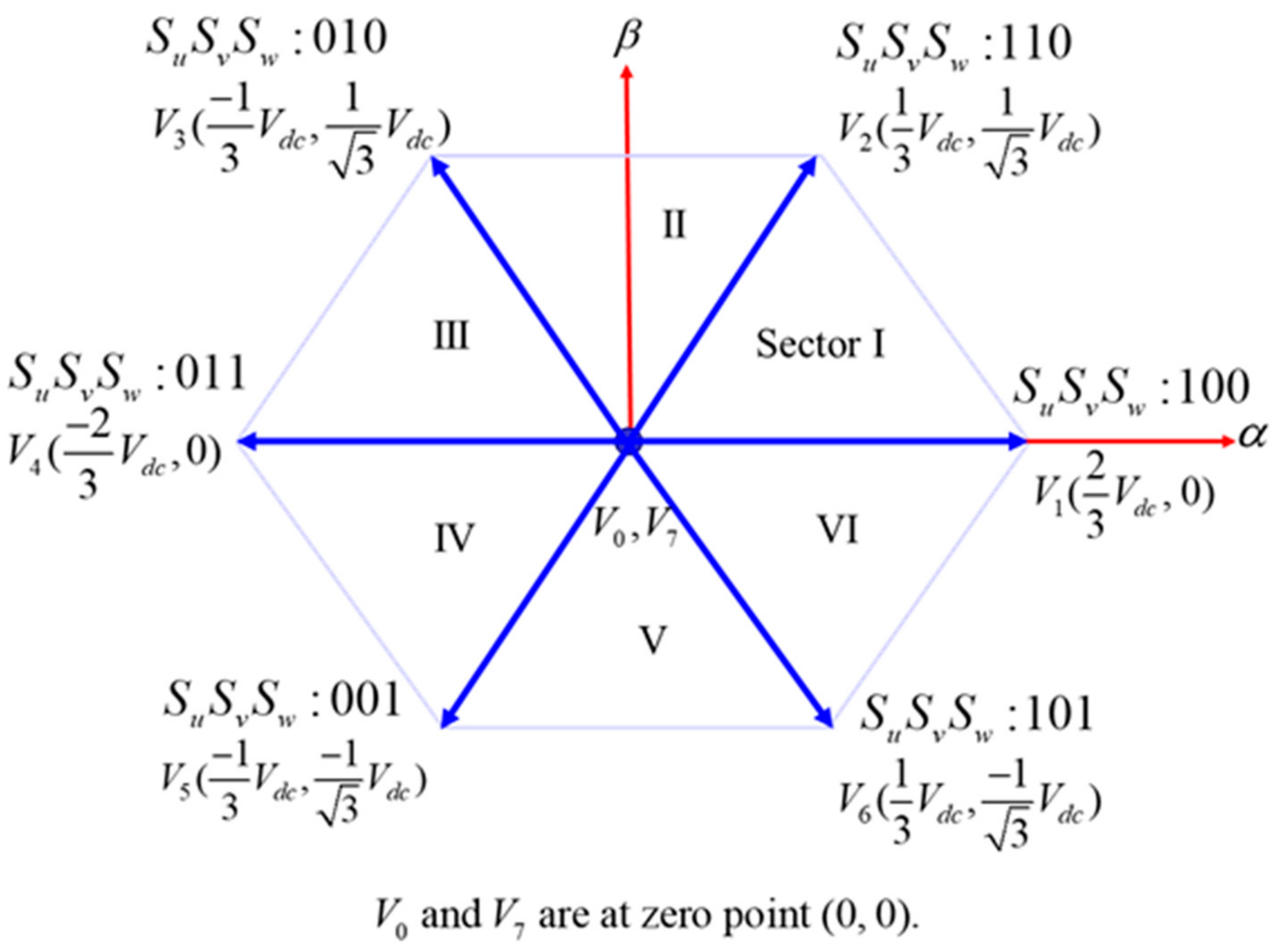
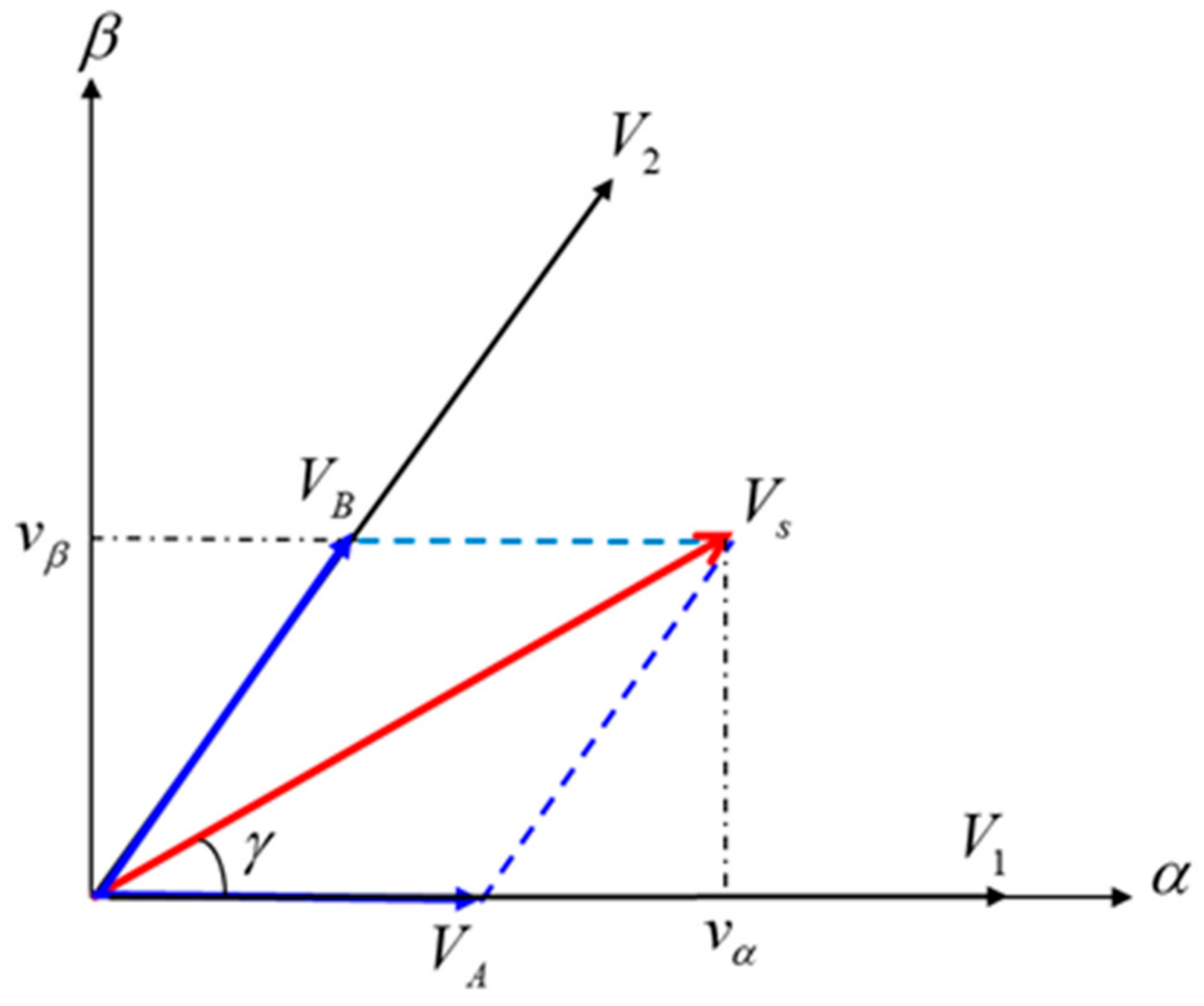
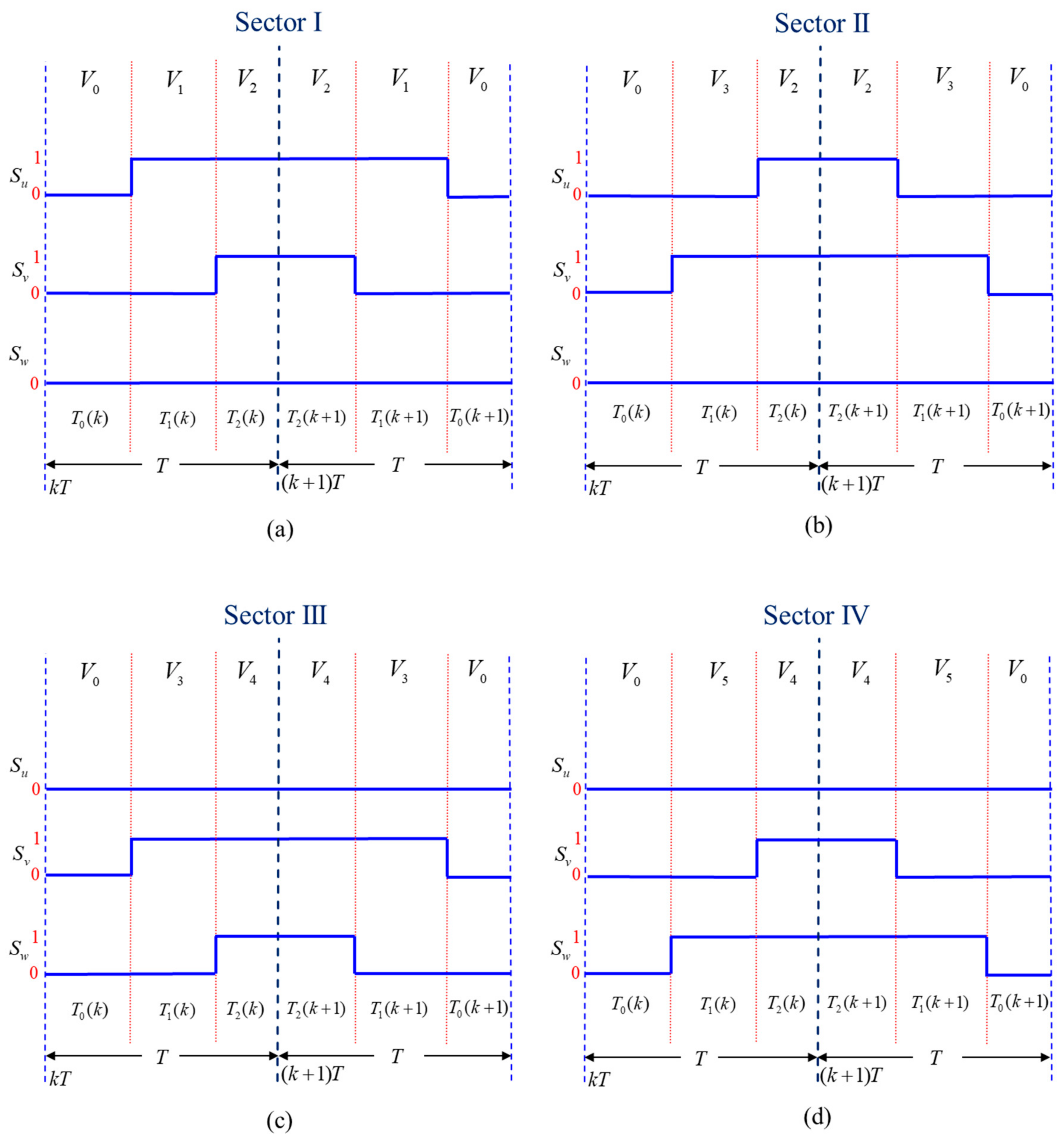
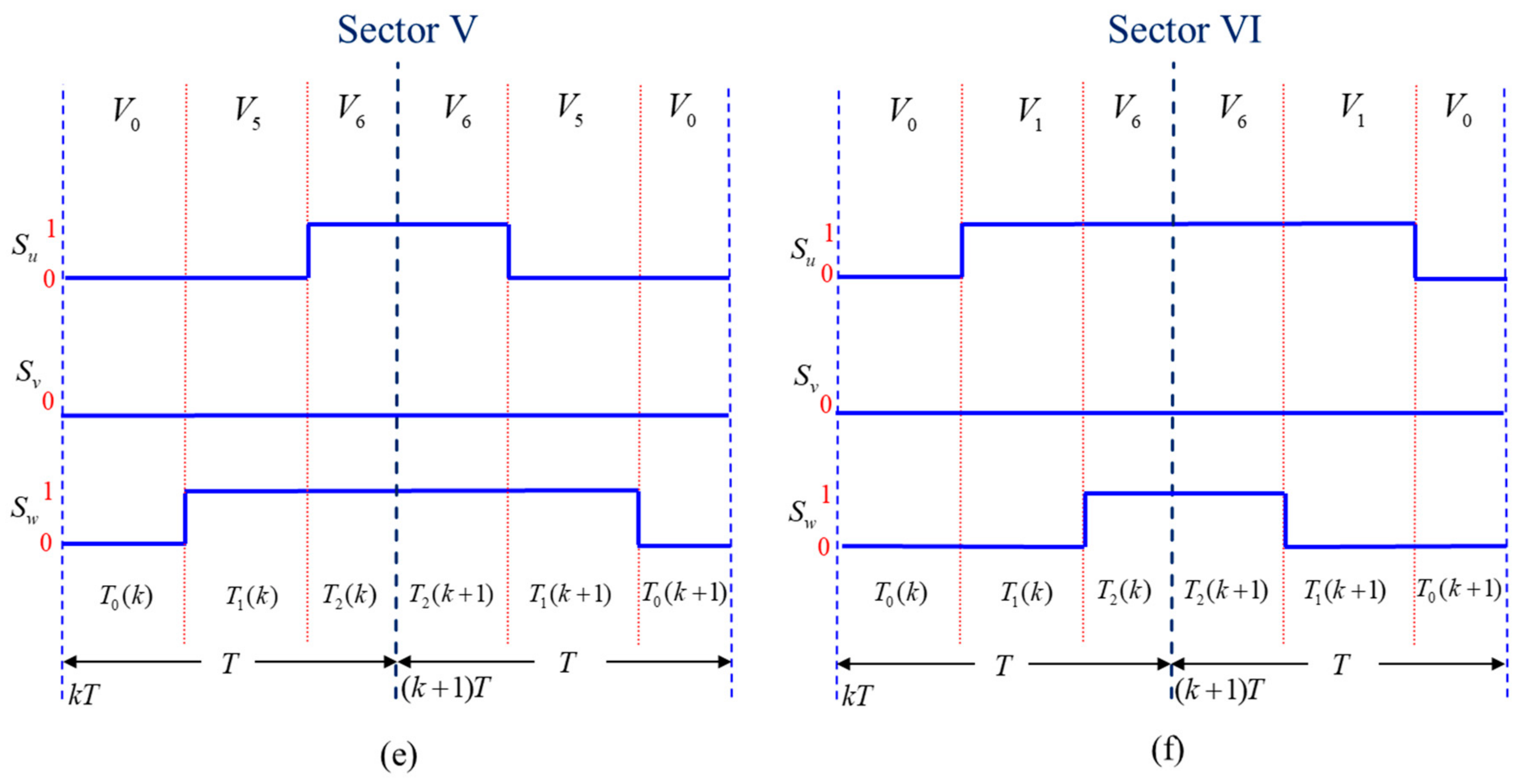
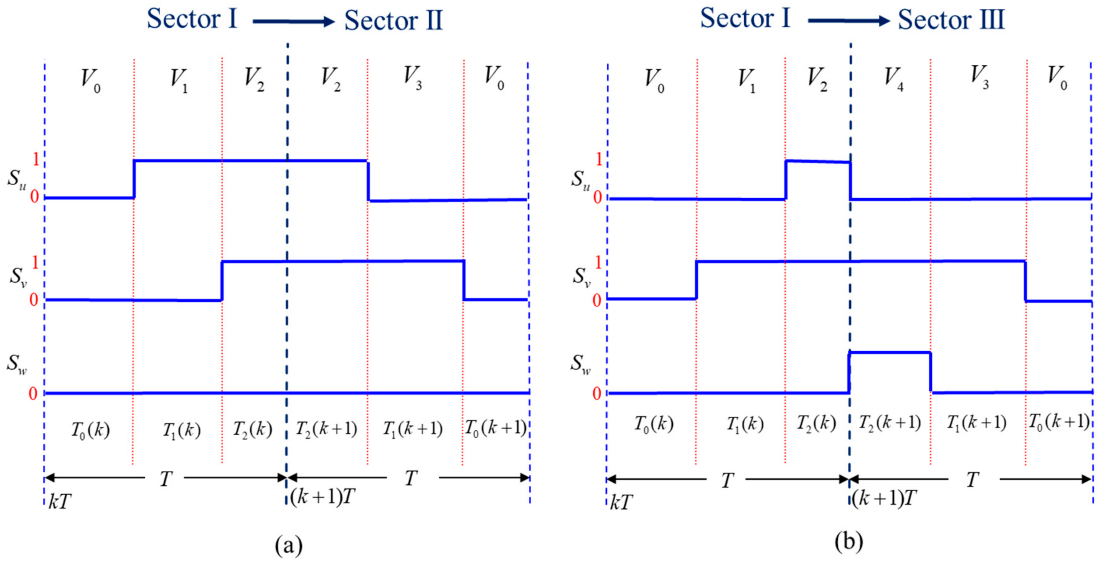
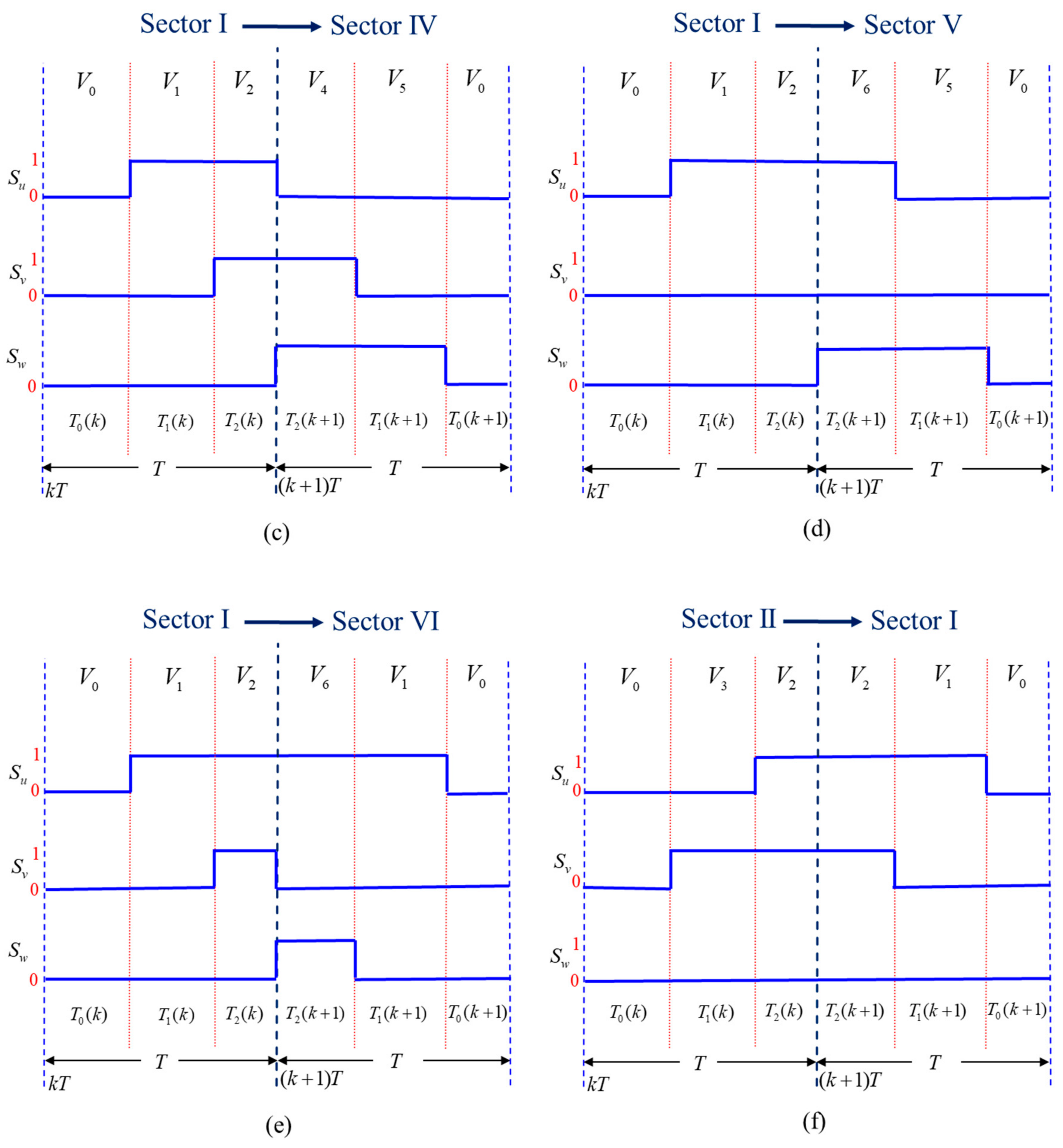
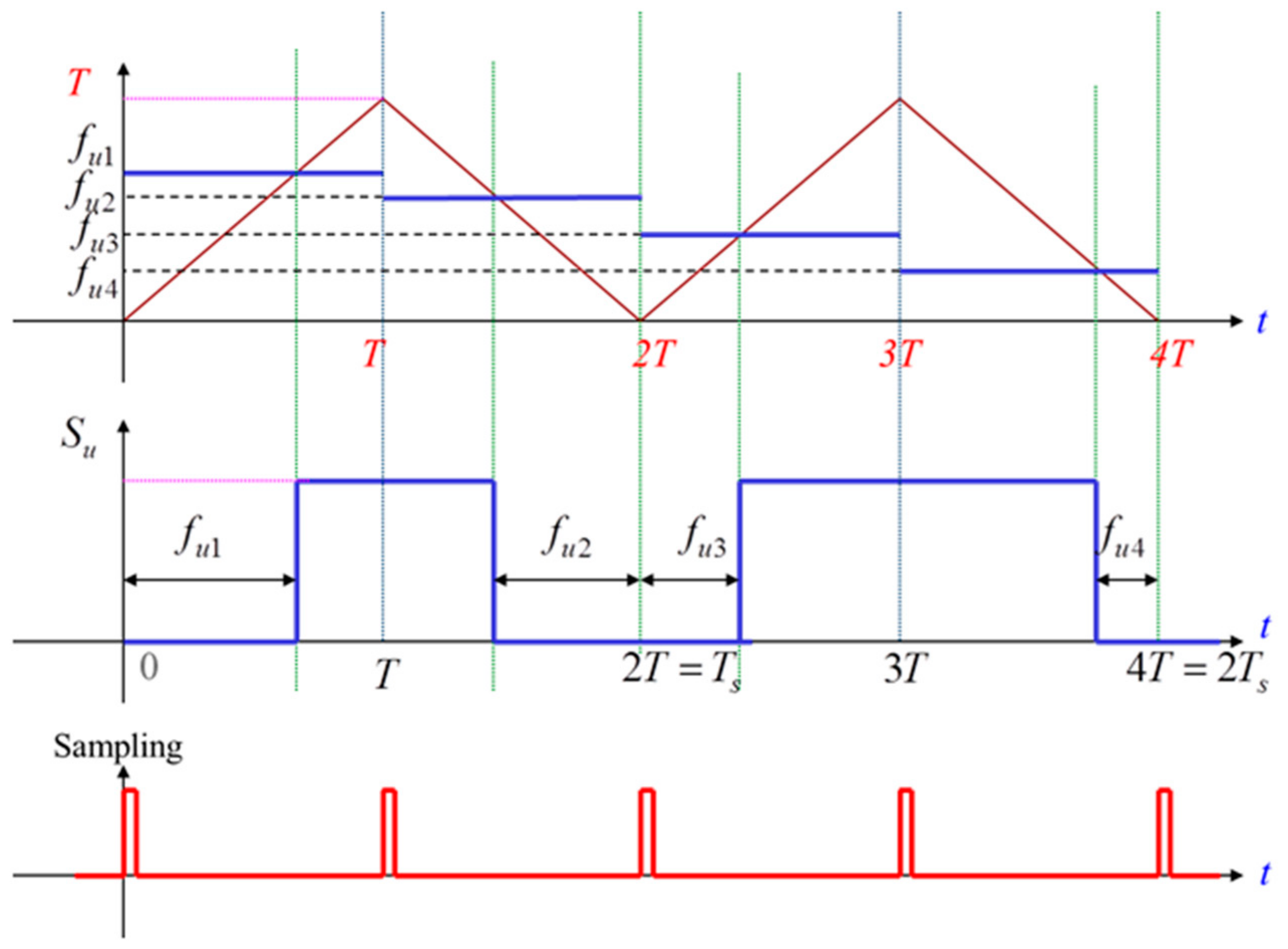
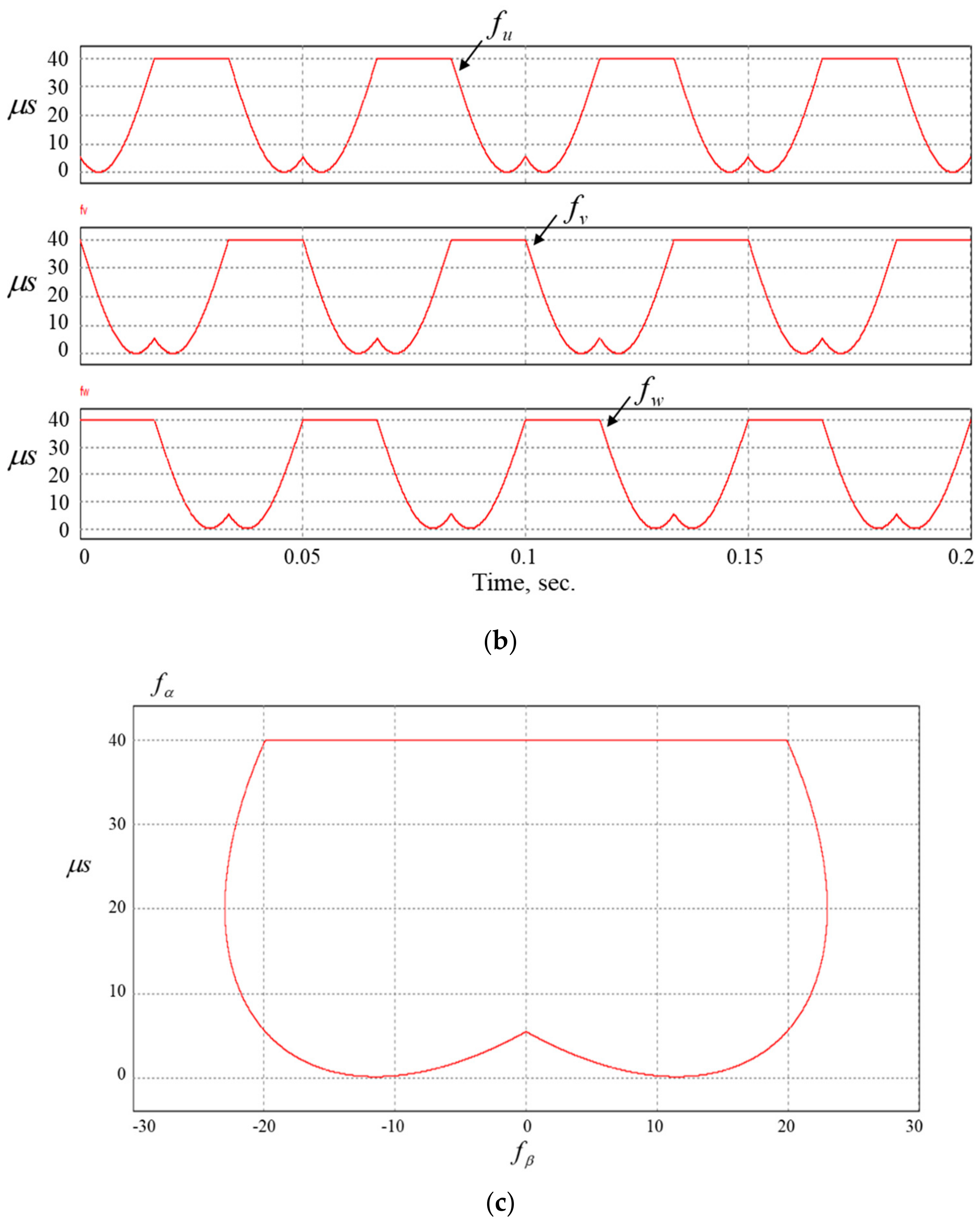
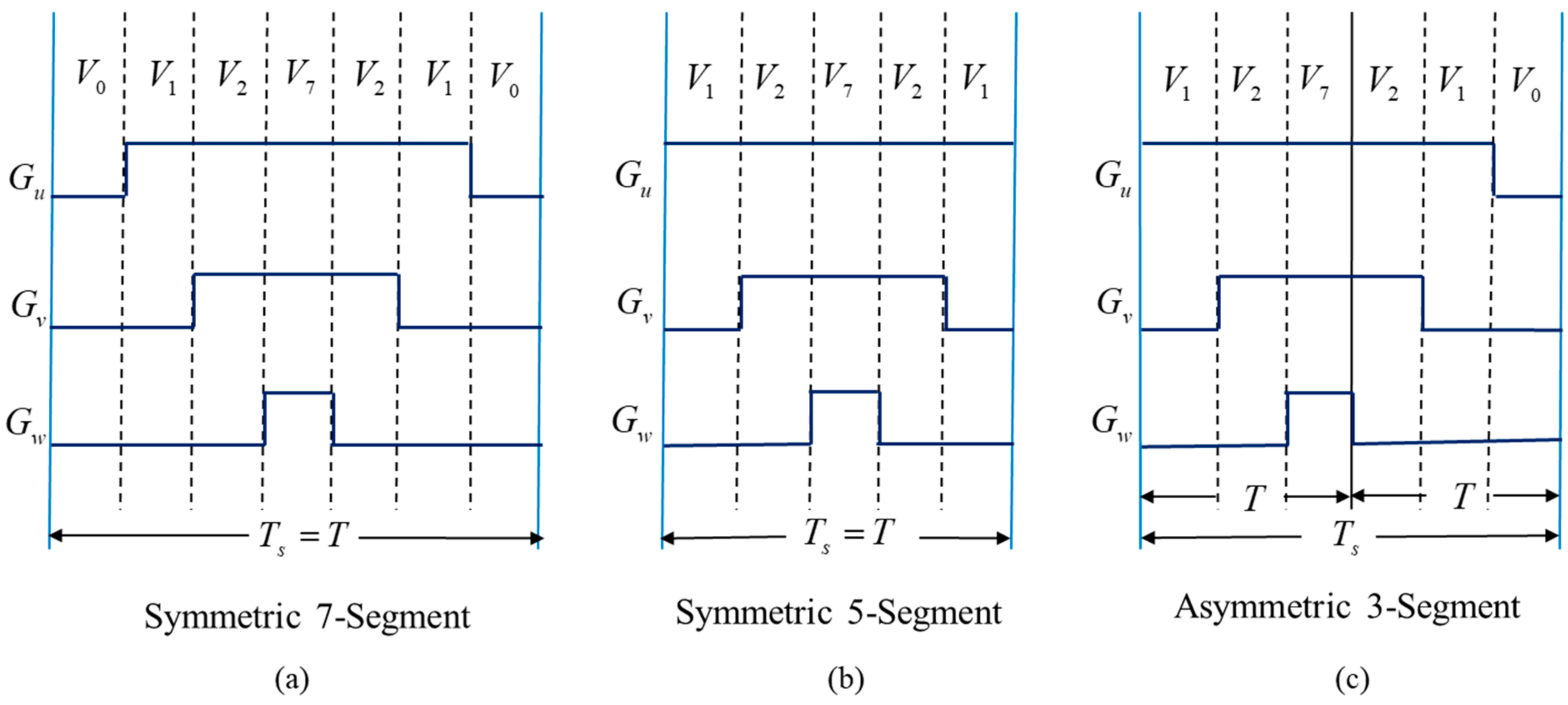
2. The Principle of the Asymmetrical Five-Segment Switching SVPWM Modulation

Firstly, as shown in Figure 2, for a three-phase PWM inverter of Y-connected AC motor with neutral point n, the three-phase stator voltages with respect to the inverter ground can be written as
v a 0 = v a n + v n 0
v b 0 = v b n + v n 0
v c 0 = v c n + v n 0
where v a n , v b n , and v c n are the three-phase voltages with respect to the neutral point of the motor, and v n 0 is the neutral-point voltage with respect to the inverter ground.
For balanced three-phase supply, it can be written as
v a n + v b n + v c n = 0
Thus, by adding (1)–(3) with the condition of (4), the neutral-point voltage with respect to the inverter ground, v n 0 , can be written as
v n 0 = 1 3 ( v a 0 + v b 0 + v c 0 )
Substituting (5) into (1)–(3) yields
v a n v b n v c n = 2 3   1 3   1 3 1 3             2 3   1 3 1 3   1 3             2 3 v a 0 v b 0 v c 0
Secondly, because the three-phase stator voltages are dependent upon (4), the inputs of the SVPWM circuit can be reduced from the three-phase variables into α-β two-axes components with the Clarke transformation given by (7).
v α v β = 1 0 0 0   1 3 1 3 v a n v b n v c n
where v α and v β are the α-β axes component voltages in the stationary reference frame. Substituting (6) into (7) yields
v α v β = 2 3 1 3   1 3 0     1 3     1 3 v a 0 v b 0 v c 0
Thus, using (8), one can get the eight output voltage vectors, V 0 V 7 , corresponding to the eight switching states of the inverter, as shown in Table 1. The resulted space vector diagram is shown in Figure 3, which is divided into six sectors from Sector I to Sector VI. As can be seen, among the eight voltage vectors, V 0 and V 7 are the null vectors and V 1 V 6 are located on the six corners of the hexagonal diagram.
The switching waveform generations of the inverter for driving an AC motor can be accomplished by rotating a reference voltage vector around the vector space. Any instance of the reference voltage vector can be produced by the two nearest adjacent vectors and a null vector in an arbitrary sector. For example, as shown in Figure 4, for providing the reference voltage vector V s in Sector I to the motor, the voltage-second balance equation in this sector determines the time length of the two adjacent active inverter states in the following:
V s T = V A T 1 + V B T 2
where T 1 and T 2 are the dwelling time length for V 1 and V 2 , respectively, and T is the sampling period, which is one half of the inverter switching period. In order to get the solution of T 1 and T 2 in (9), it follows that
v α v β T = 2 3 V d c T 1 1 0 + T 2 1 2 3 2
Thus, T 1 and T 2 can be, respectively, solved as
T 1 = 3 T V d c ( 3 2 v α 1 2 v β )
and
T 2 = 3 T V d c v β
Let
v α v β = V s cos γ sin γ
then (11) and (12) can be rewritten as the following equations [18]:
T 1 = T a 2 3 sin ( π 3 γ )
T 2 = T a 2 3 sin ( γ )
where
a = V s 2 3 V d c
Similarly, the switching time interval in the other sectors can be derived. Table 2 summaries the results, in which the condition for sector number selection is also illustrated.
For minimizing the number of switchings in a switching period, the asymmetrically alternating-reversing pulse sequence with five-segment ( V 0 V 1 V 2 V 1 V 0 ) switching technique is employed without using the null vector V 7 , as shown in Figure 5a. The pulse patterns for two consecutive sampling intervals can be configured by beginning with the null vector V 0 on the kT sampling time and also by ending with the same null vector V 0 on the (k + 1)T sampling time, where k = 1 , 3 , 5 , . The time length T 0 on the kT and (k + 1)T sampling time intervals can be different, either for T 1 or T 2 . Therefore, the PWM pulses are asymmetric with respect to the center point of the switching period. The technique benefits from one of the inverter legs not switching during a full switching period, only one inverter leg switching at a time, and only two commutations per sampling period. Thus, the number of switchings in a switching period is four and is less than the conventional symmetric seven-segment SVPWM method, in which the number of switchings in a switching period is six.
Furthermore, as can be seen from Table 2, the switch dwelling time length T 1 and T 2 are a function of the component voltages, v α and v β , the sampling period, T , and the DC bus voltage, V d c . The calculations of the functions are very simple, and hence can be easily carried out by the FPGA-based digital hardware. The pulse waveforms of the proposed asymmetric five-segment switching SVPWM scheme in other sectors are also shown in Figure 5. However, there may be the cases of the reference voltage vector travelling across the sector on the trailing sampling interval. In this case, the sector pulse pattern in the leading sampling interval must change to the next sector pulse waveforms on the trailing sampling interval. Figure 6 illustrates a pulse waveform crossing from Sector I to the other five sectors and from Sector II to I on the trailing sampling interval.
The scaled reference commands can be routed to the circuit block for the calculation of the dwelling time duration T 1 and T 2 in each sector for generating the PWM signals [17]. However, for reducing the computation complexity, an alternative method is used by calculating the firing time, which is defined as the time interval from the start to the leading edge of the PWM pulse. For example, in Sector I, the PWM firing times for the switches S u , S v and S w in the kT sampling period can be obtained as follows:
f u = T 0           = T 3 T V d c ( 3 2 v α + 1 2 v β )
f v = T 0 + T 1 = T s T 2           = T 3 T V d c v β
f w = T
where T 0 = T T 1 T 2 . The resulting equations for the PWM firing time in another sector can be obtained in the same way. Table 3 summarizes the results. As can be seen, the firing-time equations in Sector I are the same as in Sector II. They are the same in Sector III and IV and in Sector V and VI as well. Thus the circuit realization for the sectors with the same firing-time equation can share the same circuit as each other. This can simplify the circuit complexity for the implementation of the ASIC. As shown in Figure 7, the PWM pulse pattern on each phase can be generated by comparing the firing-time signal with a common center-symmetrical triangular wave with amplitude of T and period of 2T, which can be implemented by an up-down counter. The pulse is low when the firing-time signal is larger than the magnitude of the triangular wave and is high otherwise.

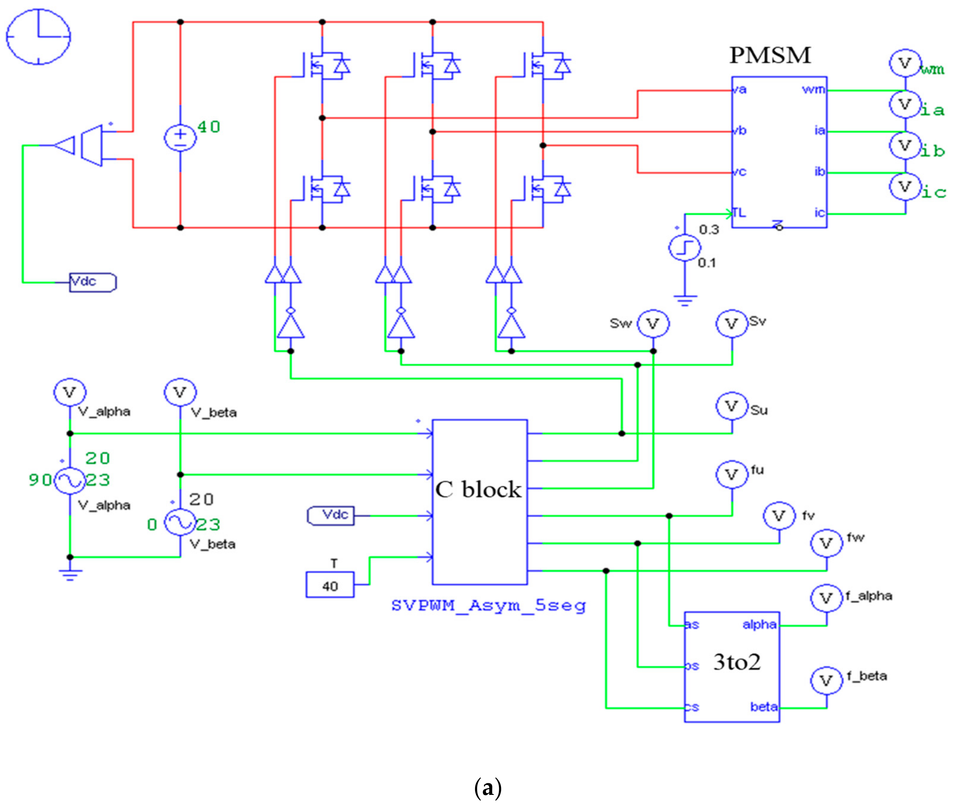
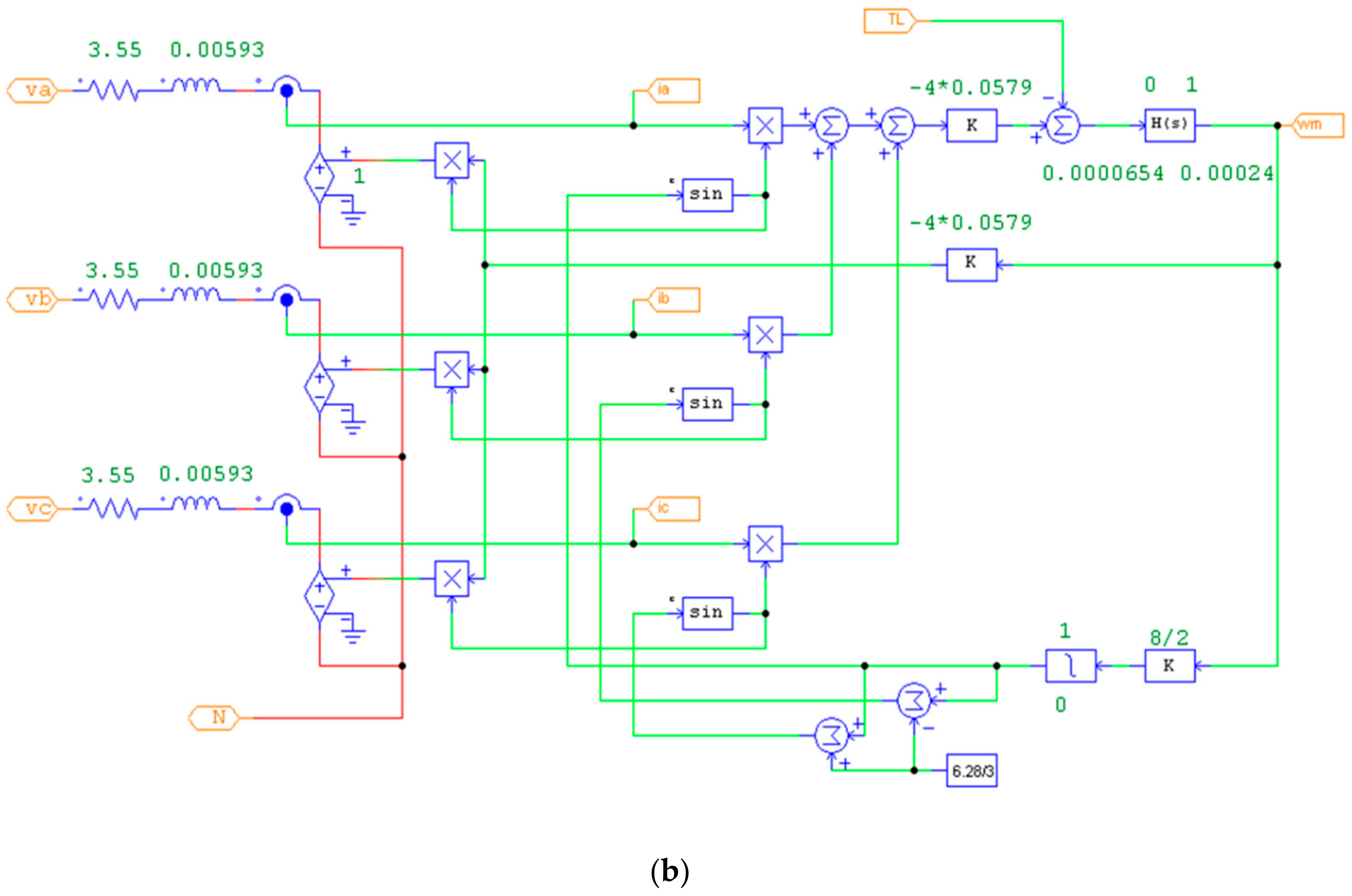
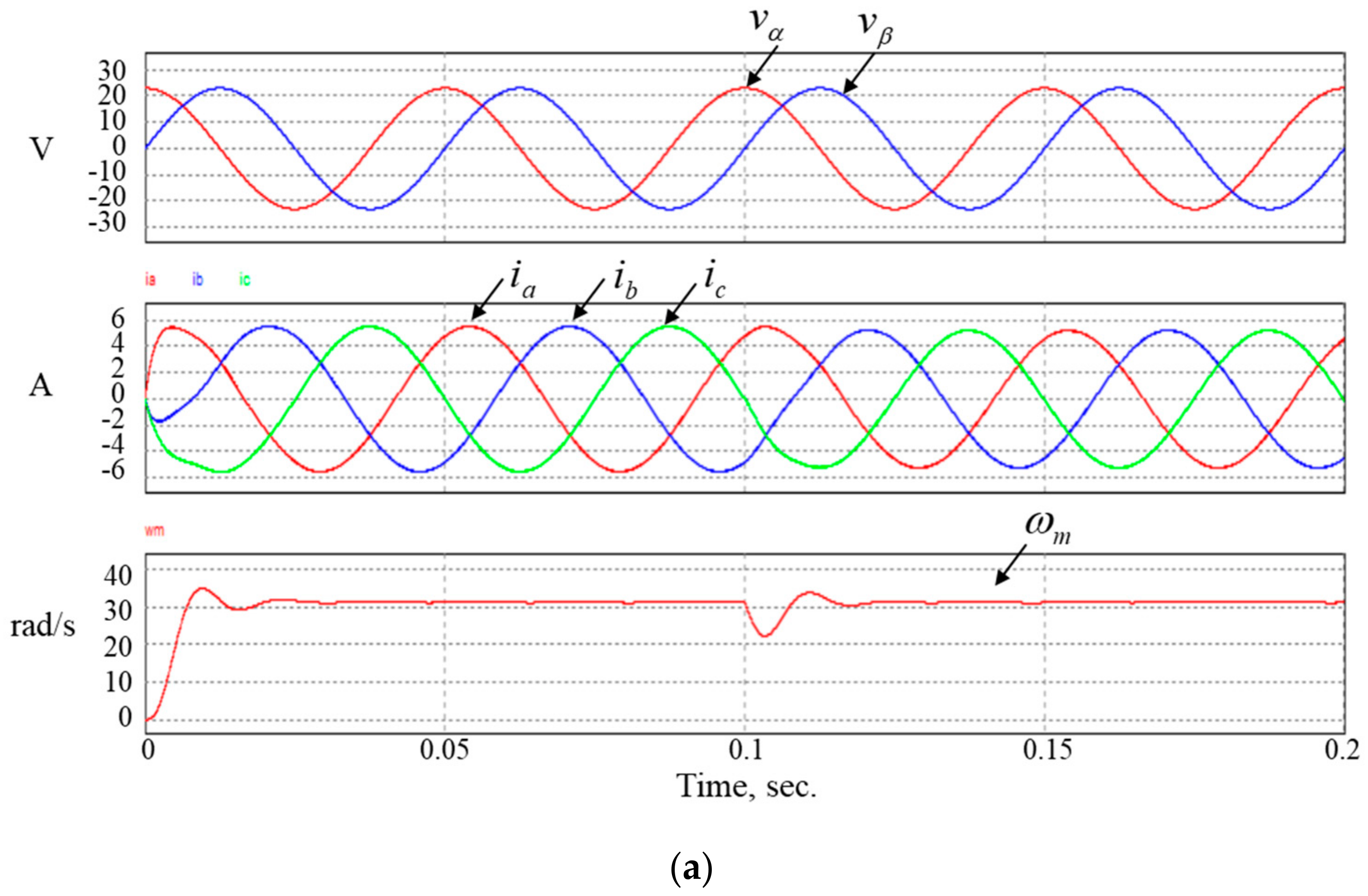
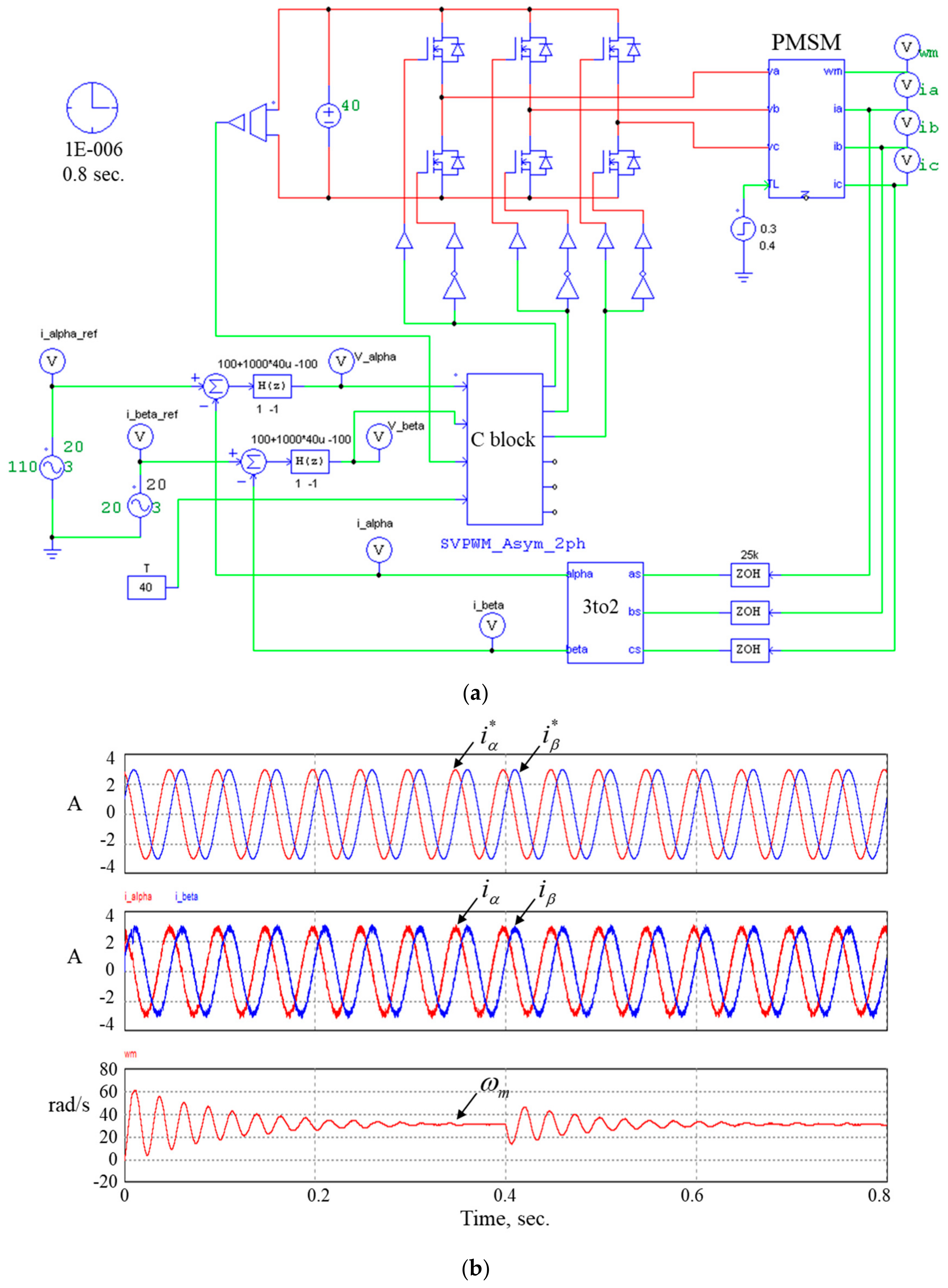
3. Simulation Verification Using PSIM

Figure 8 shows the simulation verification of the proposed asymmetric five-segment switching SVPWM modulation scheme to drive a PMSM motor by using the PSIM simulation tool, in which the PMSM motor model (Sinano 7CB30-2DE6FKS) was constructed, as shown in Figure 8b. In this simulation, the sampling period is T = 40 μ s , the DC bus voltage is V d c = 40 V , v α = 23 cos ( 40 π t ) , and v β = 23 sin ( 40 π t ) . The SVPWM modulation scheme algorithm was written in C language inside the C block function of PSIM with the flowchart shown in Figure 9. Figure 10 shows the simulation results of current and speed responses, the three-phase firing-time signals, and the firing-time signal vector trajectory with the 20 Hz voltage reference inputs given above and 0.3 Nm load torque at 0.1 s. As can be seen, the speed is 31.4 rad/s in the steady-state, which can verify the correction of the algorithm of the proposed SVPWM modulation scheme.
Figure 11 shows the simulation verification of the discrete-time current control of the PMSM motor using the proposed SVPWM scheme. A discrete-time proportional-integral (PI) controller is designed with the pulse transfer function in (20) and the zero-order holder with sampling frequency of 25 kHz, which is two times of the inverter switching frequency. As can be seen, the current responses can track the current reference with the amplitude of 3A and frequency of 20 Hz.
H ( z ) = k p + k i T k p z 1 1 z 1

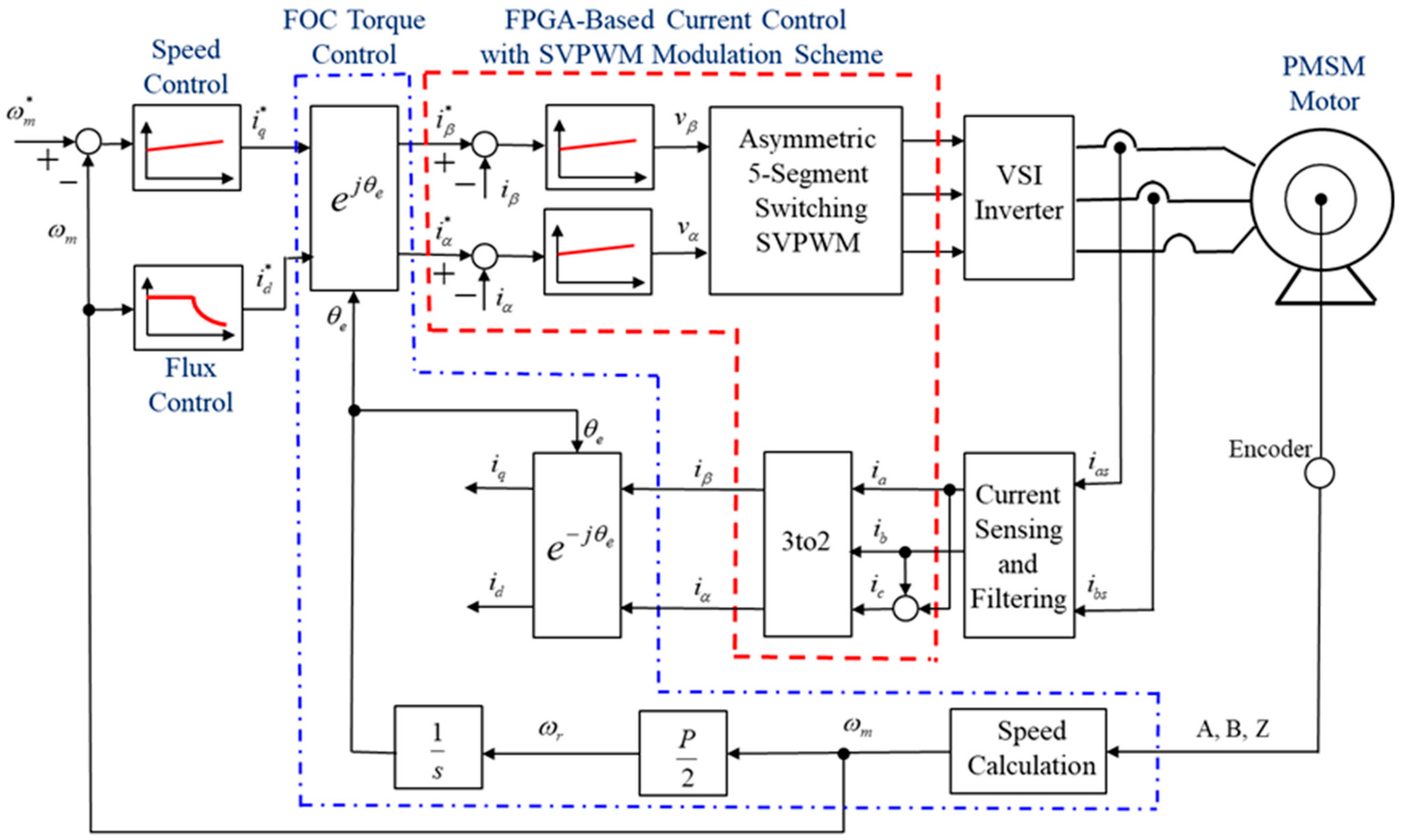
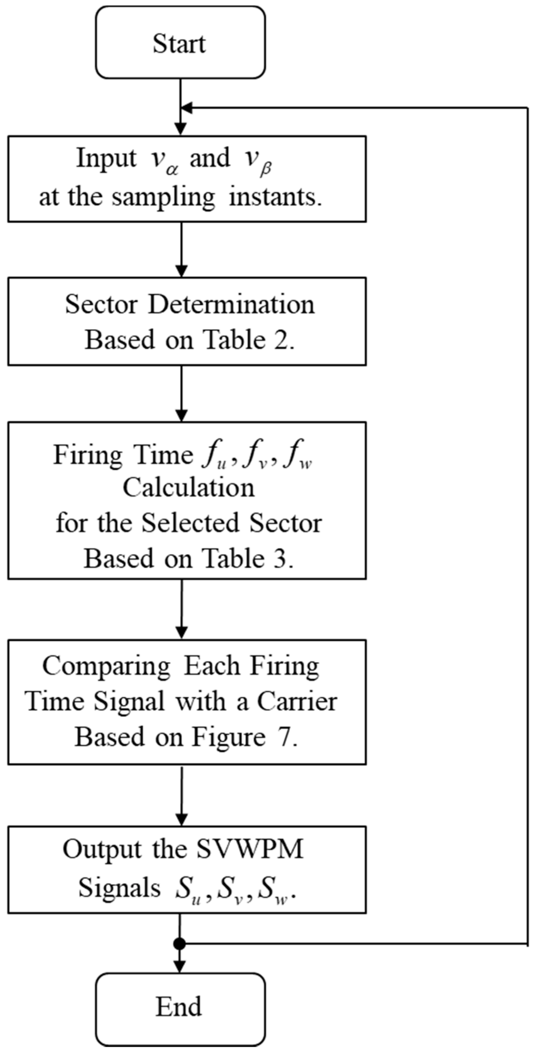
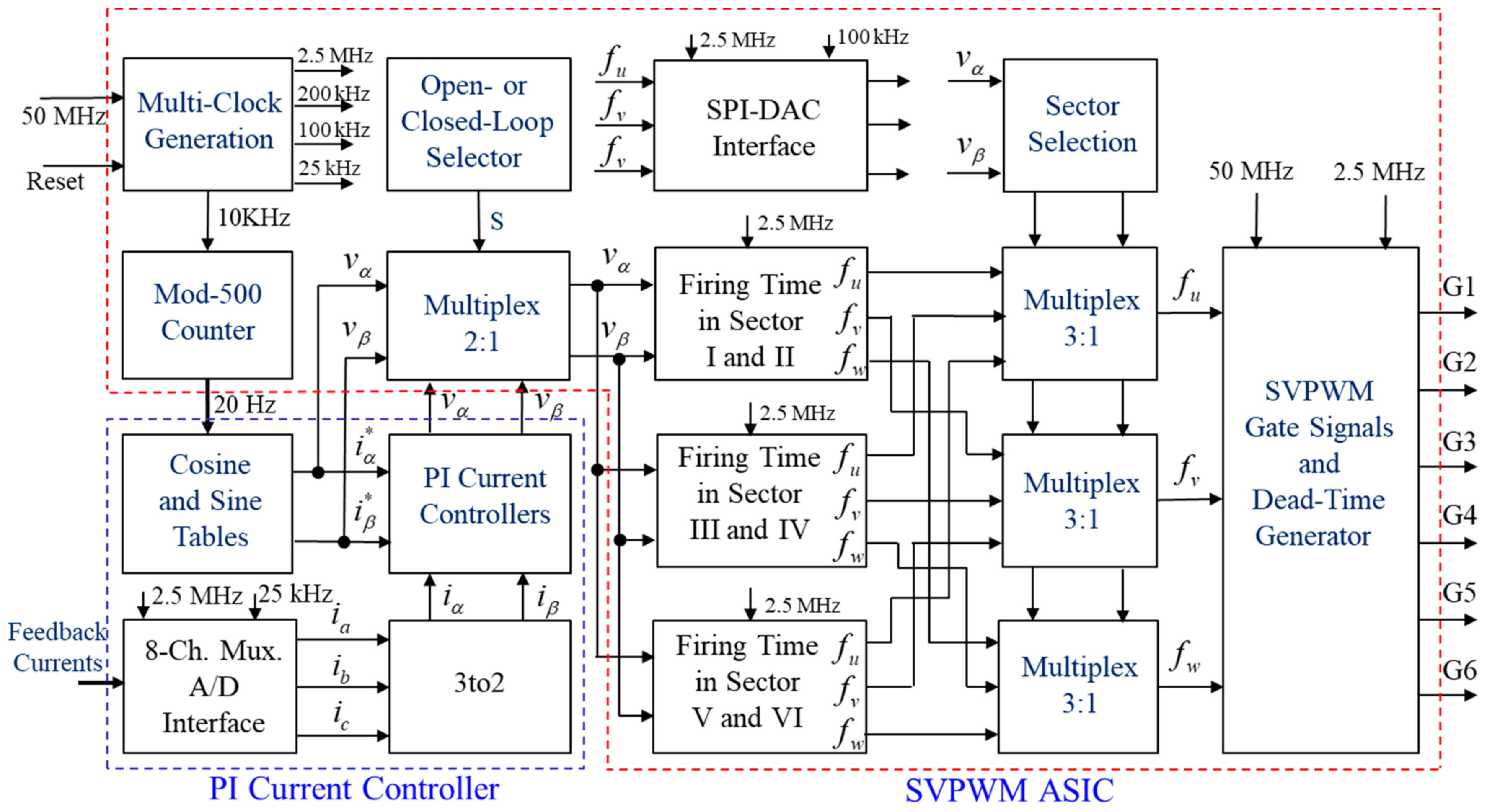
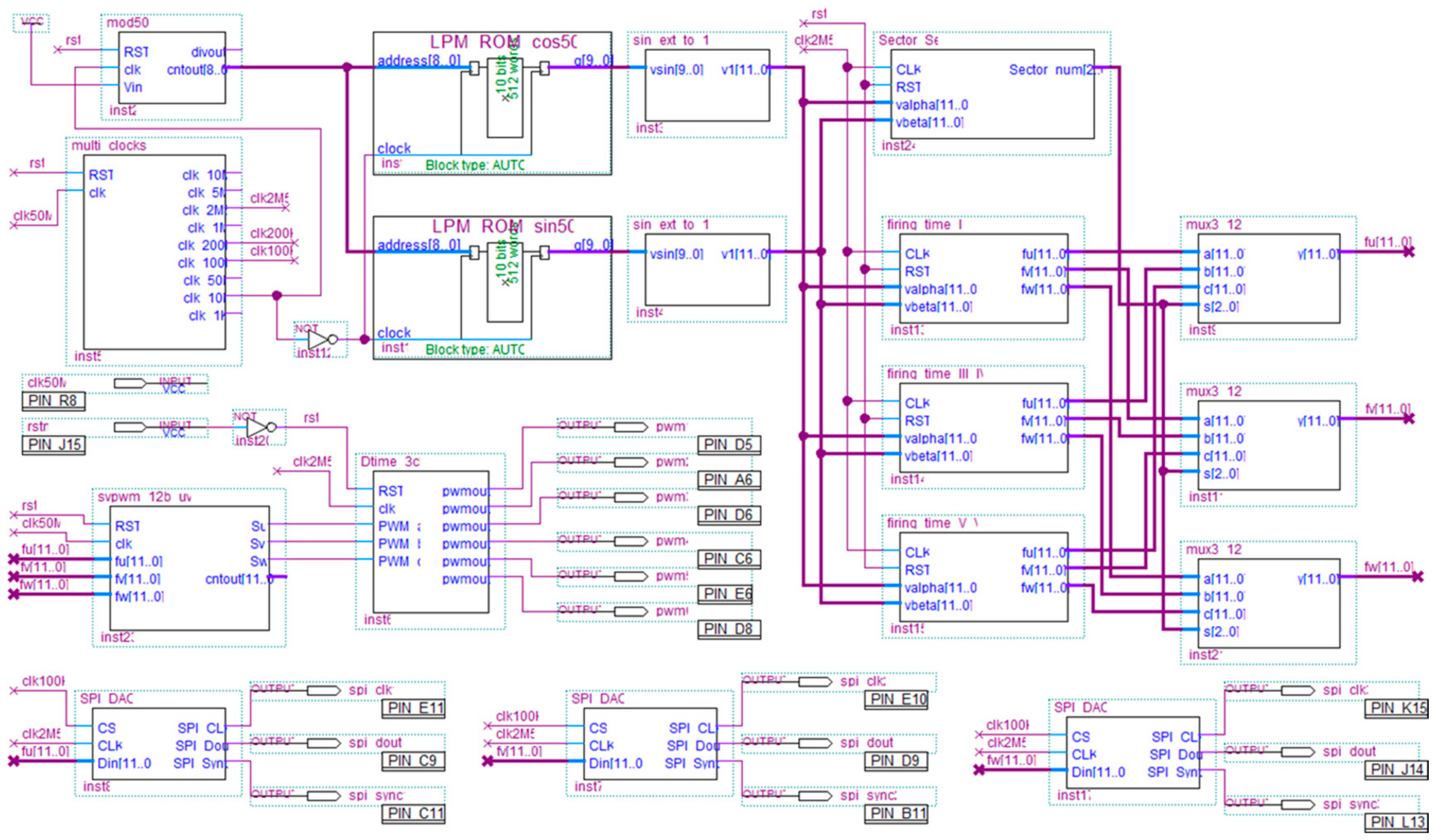
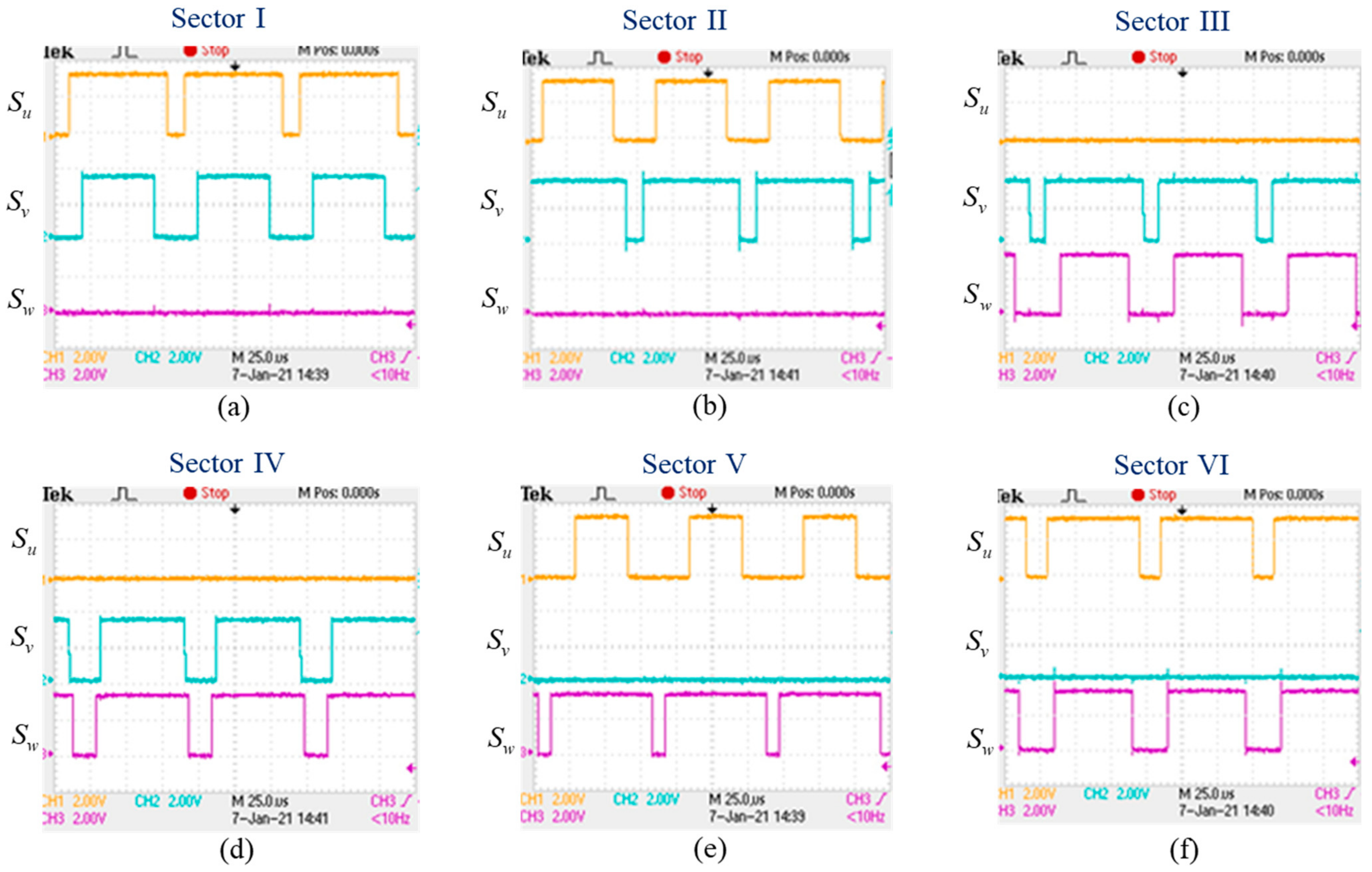
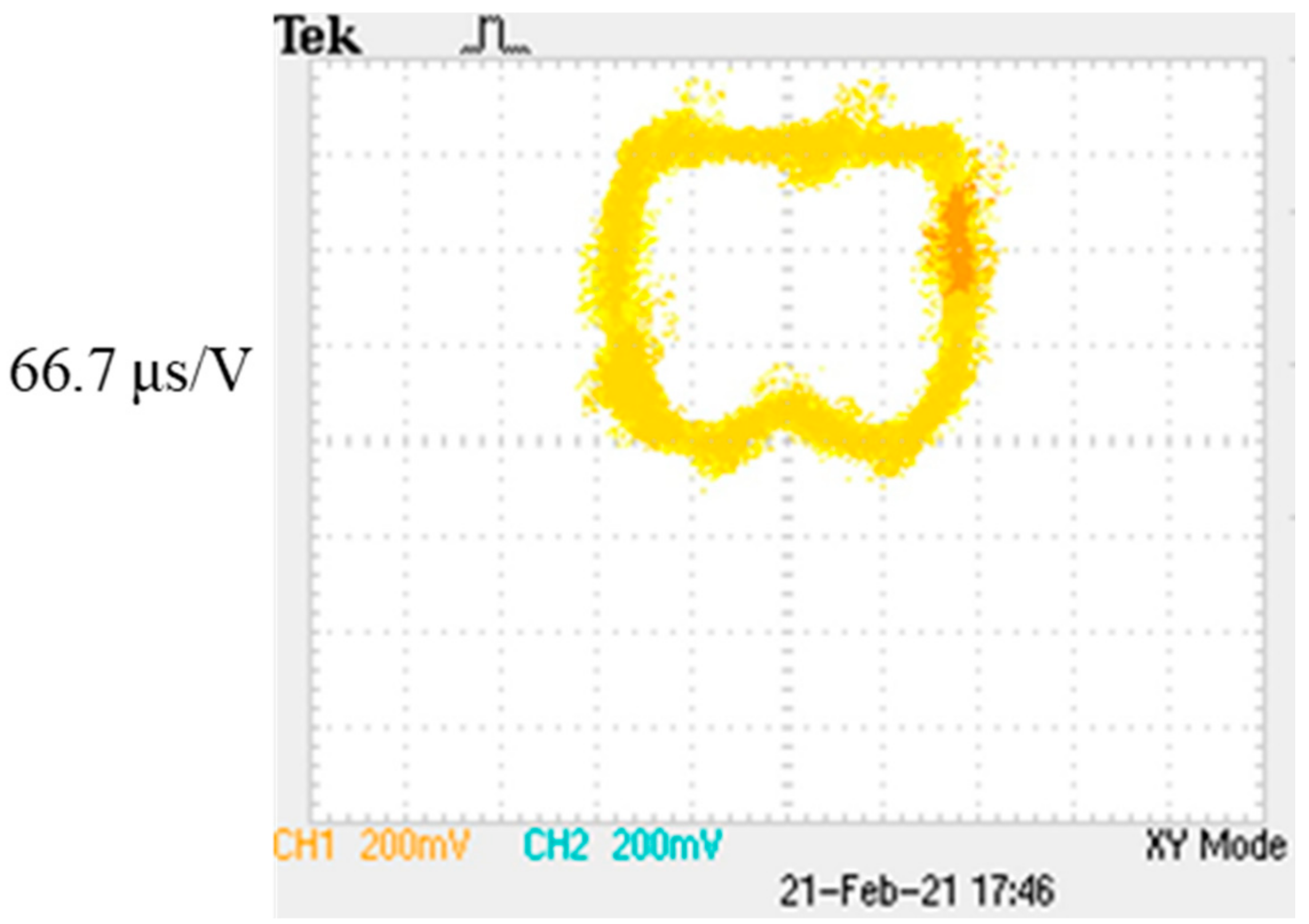
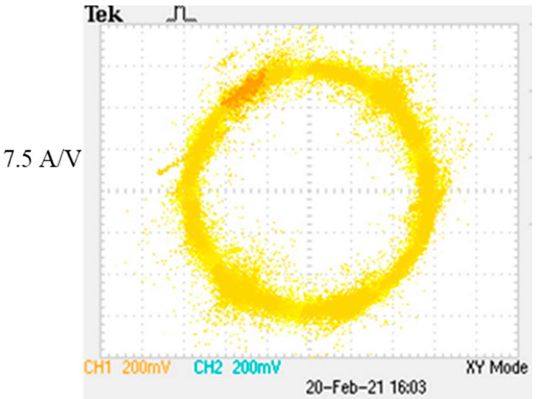
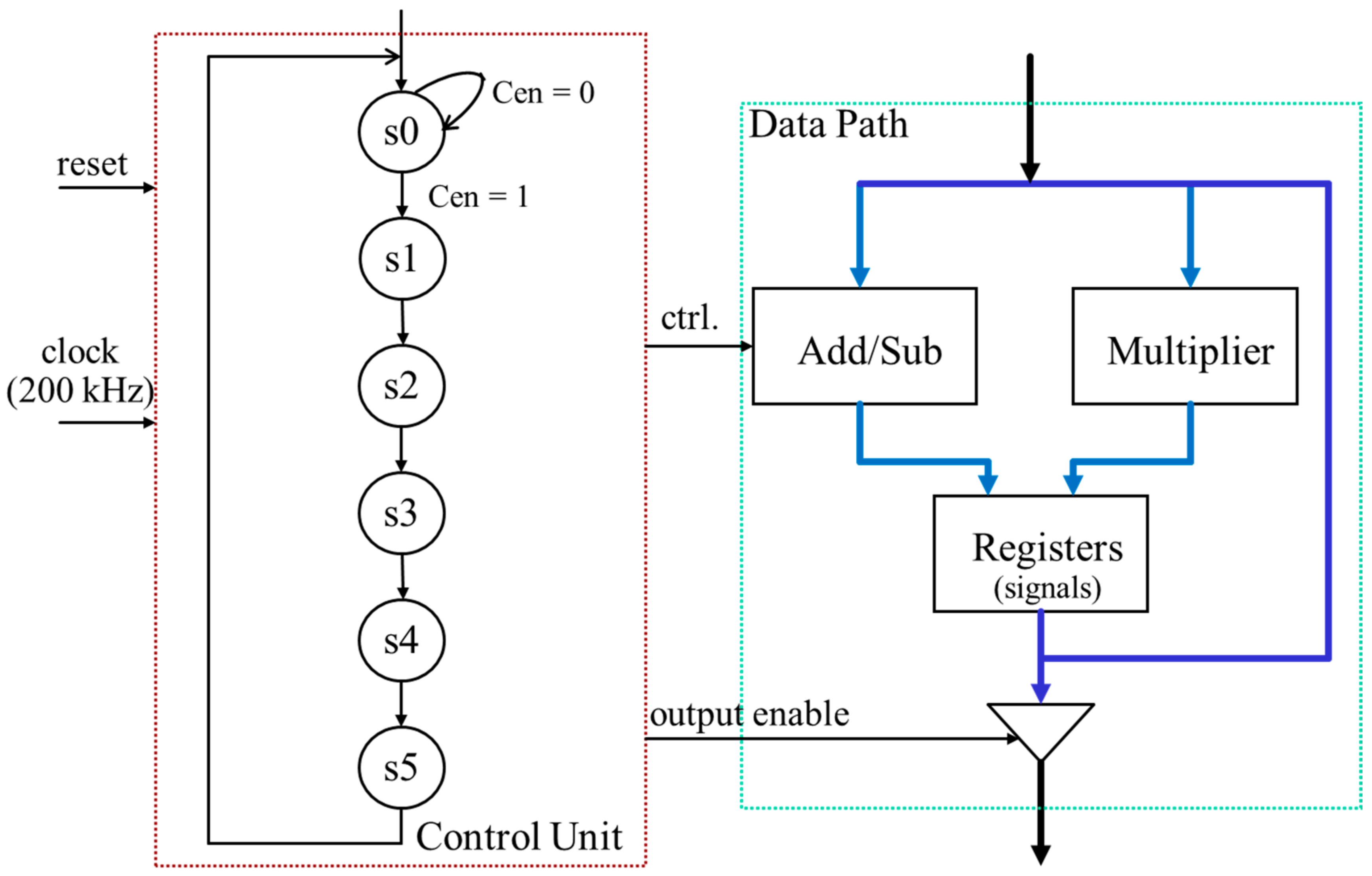
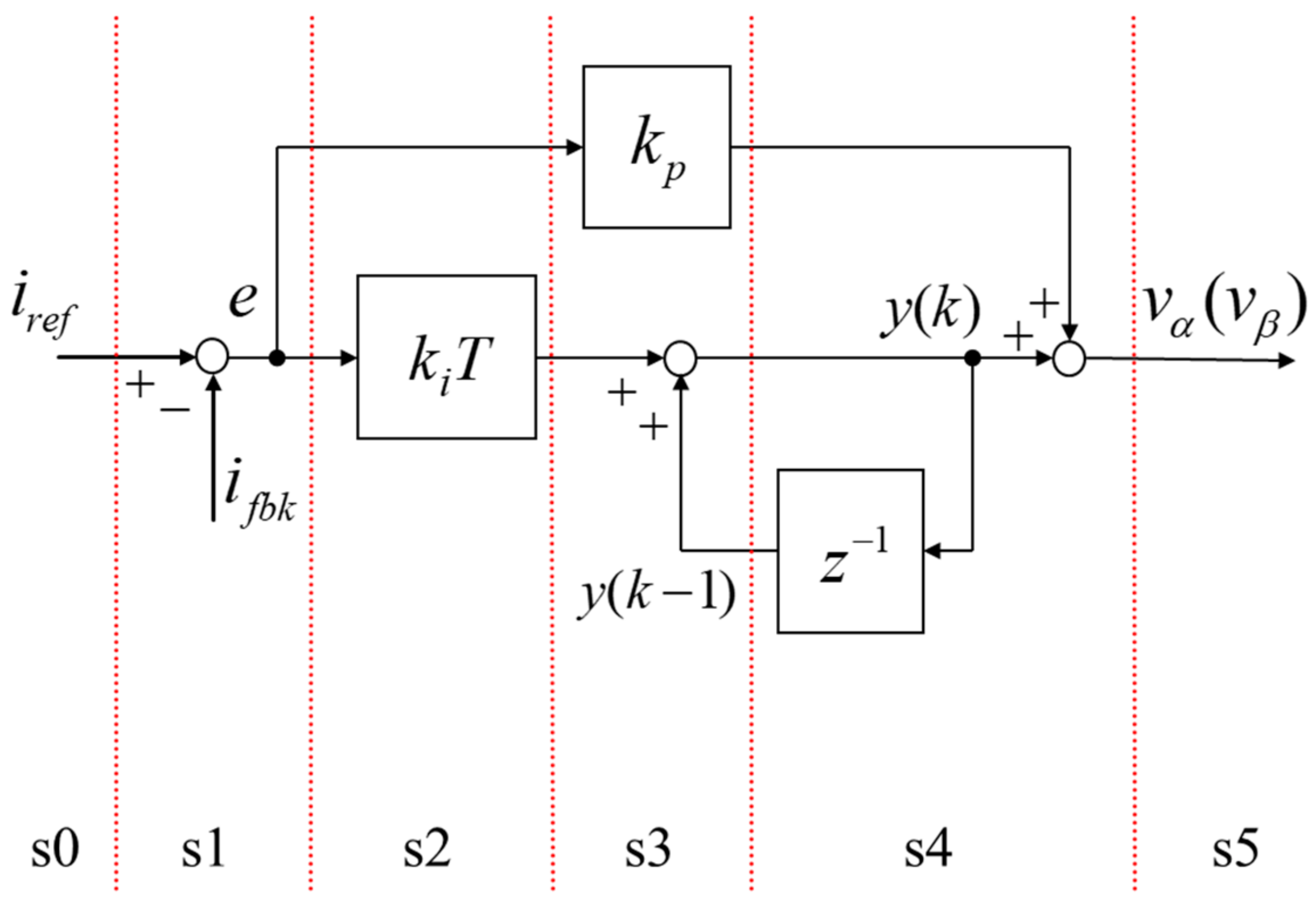
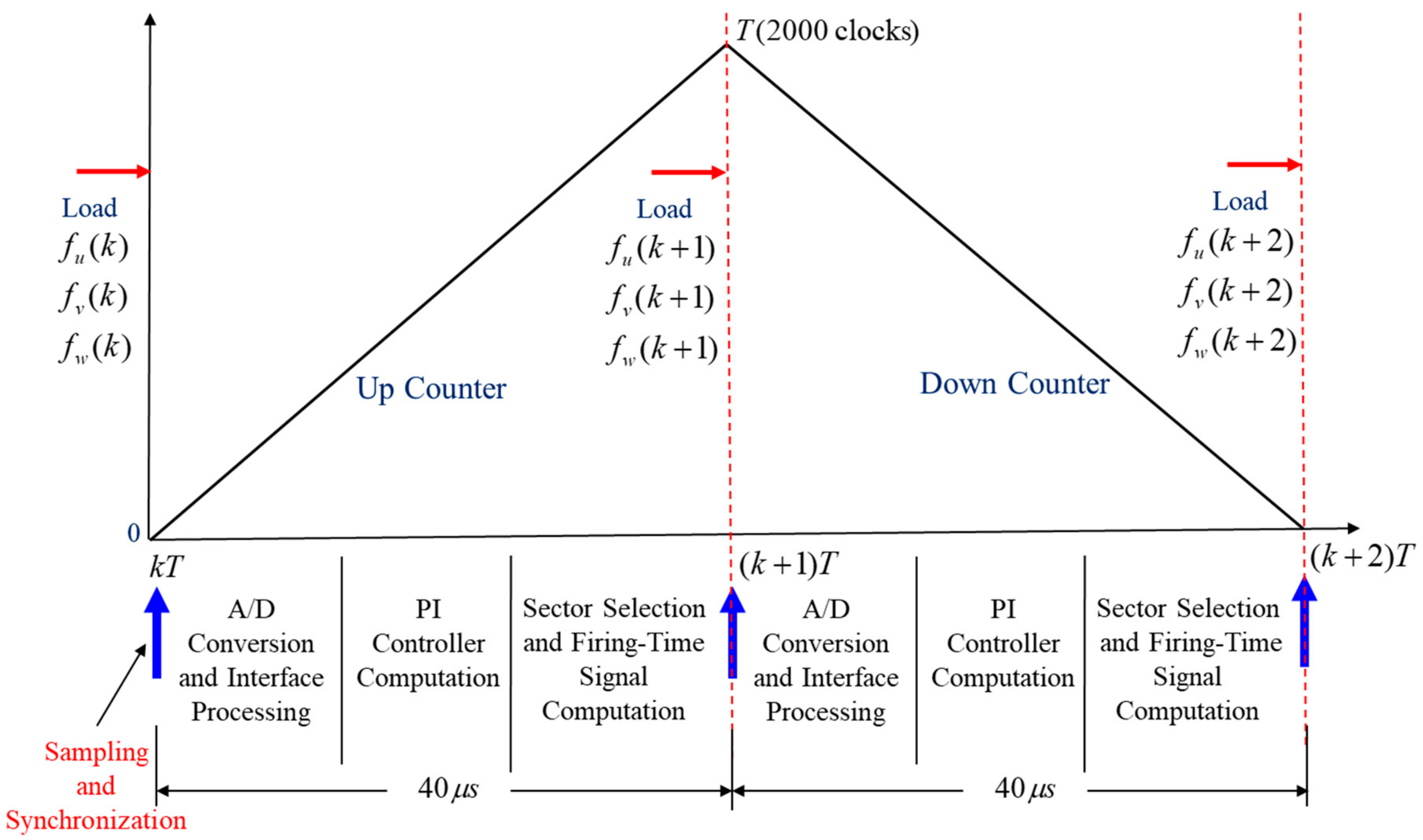
4. FPGA Implementation

A DE0-Nano FPGA control board by Terasic Inc. with Altera Cyclone IV-E device (EP4CE22F17C6) was employed for the implementation and experiment verification of the proposed current control and SVPWM ASIC for driving a PMSM servo motor (Sinano) with rated power of 300 W. Figure 12 shows the designed SVPWM ASIC structure with optional current control function included. The DE0-Nano board includes a 50 MHz oscillator, which can be used as a source clock to the designed multi-clock generation circuit to give various frequency clock signals, such as 2.5 MHz, 200 kHz, 100 kHz, and 10 kHz, for the design of the ASIC. A cosine and a sine look-up table, each with 500 words and 10 bits/word, were created by using LPM_ROM function to generate the voltage references, v α and v β , in which the frequency can be determined through the modulus-500 counter as a frequency divider. The voltage references then can be used as the inputs of the sector selection circuit according to Table 2 and the inputs of the firing time calculation circuit in each sector according to Table 3. Because some firing time equations are the same, they can be divided into three groups. The 3:1 multiplexers are used in order to select the three firing-time signals f u , f v , and f w in each sector. The 50 MHz clock is used as the input of an up-and-down counter, which counts up from zero to 2000 and then counts down to zero, for the generation of a triangular carrier signal with an 80 μ s period. The three firing time signals are then compared with the common triangular carrier counter value, respectively, to generate the three-phase SVPWM signals. A dead-time interval of 2 μ s in each phase is also inserted to generate the six gate signals to drive the inverter. A SPI-DAC interface to a DAC7513 converter was also designed to illustrate the three-phase firing time signals on the oscilloscope.
The SVPWM ASIC in the FPGA chip was designed, as shown in Figure 13, by using Altera Quartus II software development system of version 13.1. The experimental results of the SVPWM three-phase switching signals in each sector are shown in Figure 14. They are consistent with the expected pulse waveforms in Figure 5. The open-loop experiment result of the firing-time signal vector trajectory in a steady state is shown in Figure 15, which is also consistent with the simulation result in Figure 10c. Figure 16 shows the experimental result of the open-loop current vector trajectory in steady state with the SVPWM scheme. Two of the three-phase currents are sensed by using two LEM-55P current sensors and filtered through low-pass filters. The filtered currents are shifted up 1.65 V, being the inputs to an ADC128S022 A/D converter, in which the input voltage range is between zero and 3.3 V, for the feedback of the PI current control function with 25 kHz sampling frequency.
For saving the hardware resources, the computation architecture of the PI controller in the ASIC is shown in Figure 17, which has a control unit and a data path, which contains a 12-bit adder/subtracter, a 12-bit multiplier, and a limiter. The control unit is a finite state machine (FSM) which generates the control signals to the data path to control the computation procedures of the PI controller. The computation procedures of the PI controller according to the pulse transfer function in (20) are shown in Figure 18. There are five steps (s1–s5) for the computation of the PI control function. For the 25 kHz sampling frequency, the input clock frequency for the PI control function is 200 kHz. Therefore, there are eight clocks, in which three clocks are used for waiting state, needed to accomplish the computation of the PI controller. Figure 19 shows the experimental result for the closed-loop current vector trajectory in steady state with different DC bus voltage values. As can be seen, it can be a circular in the range from 55 to 63 V.

5. Discussion

Several practical aspects for the implementation of the proposed current control and SVPWM ASIC are discussed as follows:
Firstly, as shown in Figure 7, the firing-time signals are the modulating signals and used to compare with a common center-symmetrical triangular carrier wave for generating the PWM gating signals of the inverter in the proposed SVPWM scheme. This is different from the conventional SPWM implementation method, in which the sinusoidal control outputs are the modulating signals. For convenience, the firing time equation of f v in Table 3 is rewritten as follows:
f v = T 3 T V d c v β = T ( 1 3 V d c v β )
The second term on the right-hand side of the equals sign has a relationship with the duty ratio of the gating signal expressed as
d v = 3 V d c v β
Because the duty ratio is 0 d 1 , it follows that
v β V d c 3
So, the maximum value of the control signals v β or v α is V d c / 3 and is larger than V d c / 2 , which is the maximum value of the modulating signals in SPWM method. Thus, as is well known, the SVPWM method has higher voltage utilization by about 115% than the SPWM modulation method.
Secondly, the term 3 / V d c in (22) can be seen as the gain from the control signal v β to the duty ratio to generate the gating signal in the SVPWM modulation scheme. Thus, this gain can be expressed as
K s v p w m = d v v β = 3 V d c
It was found that this SVPWM gain can be included in the PI current controller parameters. So, although the firing time equations are relative to the dc bus voltage, the multiplication of the SVPWM gain to the control output signal v β is not necessary for the implementation of the firing-time signal. That means the small perturbation of the DC bus voltage will not affect the performance of the current control and SVPWM ASIC. As can be seen from the experimental results in Figure 19, the closed-loop current vector trajectory in steady state can be a circular for the dc bus voltage of 55 and 63 V, respectively. This finding makes the implementation circuit simpler.
Thirdly, although it is the digital hardware circuit for the computation of the current control and SVPWM scheme, the timing sequence during the sampling interval from the sampling of the feedback currents to the current control and firing-time signal output must be considered for the synchronization, as shown in Figure 20. The computation of the timing signals must be completed before the next sampling time. The resulted firing-time signal values are then loaded into the PWM signal generation circuit for the comparison with an up-down counter at the next sampling time in which the counter starts to count up from zero or count down from 2000.
Fourthly, the conventional SVPWM scheme including the symmetric seven-segment technique, symmetric five-segment technique, and asymmetric three-segment technique are shown in Figure 21. As can be seen, the symmetric five-segment technique has four switching times and is the lowest during a switching period, so the switching loss of the scheme is significantly reduced in comparison with the others. However, in the asymmetric three-segment technique, the sampling frequency can be doubled at a certain switching frequency. The proposed asymmetric five-segment technique can not only have the advantages of minimum switching times, but also can double the sampling frequency in the current control loop so as to improve the control performance.

6. Conclusions

In this work, the design and implementation of an FPGA-based SVPWM ASIC with an asymmetric five-segment switching scheme for AC motor drives have been performed. The inverter switch dwelling and firing times on each sector have been derived. It was found that the firing-time equations in Sector I and II are the same. They are the same in Sector III and IV and in Sector V and VI as well. These finding allow us to simplify the circuit complexity for the implementation of the ASIC. Compared with the conventionally symmetric seven-segment three-phase switching scheme, the inverter switching times and power loss of this proposed scheme can not only be reduced by 33%, but also the asymmetric characteristics mean that the reference voltage command signal can be given in the half period of the PWM switching time interval. Therefore, one can design the closed-loop current control while doubling the sampling frequency, hence increasing the bandwidth, and allowing the motor drive system with better dynamic response. For the verification of the proposed SVPWM modulation scheme, the closed-loop current control function in the stationary reference frame has been also included in the design of the ASIC. The ASIC function is firstly verified by using the PSIM simulation tool. Then, a DE0-nano FPGA control board has been employed to drive a 300 W PMSM AC motor for the experimental verification. The simulation and experimental results show the performance of the proposed SVPWM ASIC both in the open-loop pulse-width modulation and in the current control loop. The proposed current control and SVPWM ASIC can not only be used in PMSM motor drives, but can also be applied in other AC motor drives.

Author Contributions

Conceptualization, M.-F.T. and C.-S.T.; methodology, M.-F.T.; software, P.-J.C.; validation, M.-F.T., C.-S.T. and P.-J.C.; formal analysis, M.-F.T.; investigation, M.-F.T.; resources, M.-F.T. and P.-J.C.; data curation, M.-F.T.; writing—original draft preparation, M.-F.T.; writing—review and editing, M.-F.T. and C.-S.T.; visualization, M.-F.T.; supervision, C.-S.T.; project administration, C.-S.T.; funding acquisition, M.-F.T. All authors have read and agreed to the published version of the manuscript.

Funding

This research was funded by Project number: MUST-110-mission-3, from Ministry of Education (MOE), Taiwan.

Conflicts of Interest

The authors declare no conflict of interest.

References

  1. Abouzeid, A.F.; Guerrero, J.M.; Endemaño, A.; Muniategui, I.; Ortega, D.; Larrazabal, I.; Briz, F. Control strategies for induction motors in railway traction applications. Energies 2020, 13, 700. [Google Scholar] [CrossRef] [Green Version]
  2. Sieklucki, G. An Investigation into the Induction Motor of Tesla Model S Vehicle. In Proceedings of the IEEE 2018 International Symposium on Electrical Machines (SME 2018), Miyazaki, Japan, 10–13 June 2018. [Google Scholar]
  3. Liu, T.-H.; Ahmad, S.; Mubarok, M.S.; Chen, J.-Y. Simulation and implementation of predictive speed controller and position observer for sensorless synchronous reluctance motors. Energies 2020, 13, 2712. [Google Scholar] [CrossRef]
  4. Lin, C.-H. Permanent-magnet synchronous motor drive system using backstepping control with three adaptive rules and revised recurring sieved pollaczek polynomials neural network with reformed grey wolf optimization and recouped controller. Energies 2020, 13, 5870. [Google Scholar] [CrossRef]
  5. Ferdiansyah, I.; Rusli, M.R.; Praharsena, B.; Toar, H.; Ridwan; Purwanto, E. Speed Control of Three Phase Induction Motor Using Indirect Field Oriented Control Based on Real-Time Control System. In Proceedings of the IEEE 2018 10th International Conference on Information Technology and Electrical Engineering (ICITEE 2018), Bali, Indonesia, 24–26 July 2018. [Google Scholar]
  6. Rosa, F.C.; Bim, E. A constrained non-linear model predictive controller for the rotor flux-oriented control of an induction motor drive. Energies 2020, 13, 3899. [Google Scholar] [CrossRef]
  7. Alonge, F.; Cirrincione, M.; D’Ippolito, F.; Pucci, M.; Sferlazza, A. Robust active disturbance rejection control of induction motor systems based on additional sliding mode component. IEEE Trans. Ind. Electron. 2017, 64, 5608–5621. [Google Scholar] [CrossRef]
  8. De Santana, E.S.; Bim, E.; do Amaral, W.C. A predictive algorithm for controlling speed and rotor flux of induction motor. IEEE Trans. Ind. Electron. 2008, 55, 4398–4407. [Google Scholar] [CrossRef]
  9. Rosa, F.C.; Lima, F.; Fumagalli, M.A.; Bim, E. Evolving fuzzy controller applied in indirect field oriented control of induction motor. In Proceedings of the 2016 IEEE International Conference on Industrial Technology, Taipei, Taiwan, 14–17 March 2016; pp. 1452–1457. [Google Scholar]
  10. Merabet, A.; Ouhrouche, M.; Bui, R.T. Nonlinear predictive control with disturbance observer for induction motor drive. In Proceedings of the 2006 IEEE International Symposium on Industrial Electronics, Montreal, QC, Canada, 9–13 July 2006; Volume 1, pp. 86–91. [Google Scholar]
  11. Tsai, M.-F.; Tseng, C.-S.; Lin, B.-Y. Phase voltage-oriented control of a PMSG wind generator for unity power factor correction. Energies 2020, 13, 5693. [Google Scholar] [CrossRef]
  12. Raghuwanshi, S.S.; Khare, V.; Gupta, K. Analysis of SPWM VSI fed AC drive using different modulation index. In Proceedings of the International Conference on Information, Communication, Instrumentation and Control (ICICIC), Indore, India, 17–19 August 2017. [Google Scholar]
  13. Hazari, M.R.; Effat Jahan, E.; Mannan, M.A.; Tamura, J. Artificial neural network based speed control of an SPWM-VSI fed induction motor with considering core loss and stray load losses. In Proceedings of the IEEE International Conference on Electrical Machines and Systems (ICEMS), Chiba, Japan, 13–16 November 2016. [Google Scholar]
  14. Szabo, C.; Szoke, E.; Szekely, N.C.; Zacharias, V.; Imecs, M. Analysis of current-feedback PWM procedures based on hysteresis and current-carrier-wave control for VSI-fed induction motor drive. In Proceedings of the International Aegean Conference on Electrical Machines and Power Electronics (ACEMP) & International Conference on Optimization of Electrical and Electronic Equipment (OPTIM), Istanbul, Turkey, 27–29 August 2019. [Google Scholar]
  15. Harikrishnan, R.; Ashni, E.G. Direct torque control of PMSM using hysteresis modulation, PWM and DTC PWM based on PI control for EV—A comparative analysis between the three strategies. In Proceedings of the IEEE International Conference on Intelligent Computing, Instrumentation and Control Technologies (ICICICT), Kerala, India, 5–6 July 2019. [Google Scholar]
  16. Tzou, Y.-Y.; Hsu, H.-J.; Kuo, T.-S. FPGA-based SVPWM control IC for 3-phase PWM inverters. In Proceedings of the 22nd International Conference on Industrial Electronics, Control, and Instrumentation (IECON 1996), Taipei, Taiwan, 9 August 1996; pp. 138–143. [Google Scholar]
  17. Tzou, Y.-Y.; Hsu, H.-J. FPGA realization of space-vector PWM control IC for three-phase PWM inverters. IEEE Trans. Power Electron. 1997, 12, 953–963. [Google Scholar] [CrossRef]
  18. Bowes, S.R.; Lai, Y.-S. The relationship between space-vector modulation and regular-sampled PWM. IEEE Trans. Ind. Electron. 1997, 44, 670–679. [Google Scholar] [CrossRef]
  19. Tzou, Y.-Y.; Lin, S.-Y. Fuzzy-tuning current-vector control of a three-phase PWM inverter for high-performance AC drives. IEEE Trans. Ind. Electron. 1998, 45, 782–791. [Google Scholar] [CrossRef]
  20. Hava, A.M.; Kerkman, R.J.; Lipo, T.A. Simple analytical and graphical methods for carrier-based PWM-VSI drives. IEEE Trans. Power Electron. 1999, 14, 49–61. [Google Scholar] [CrossRef]
  21. Trzynadlowski, A.M.; Bech, M.M.; Blaabjerg, F.; Pedersen, J.K. An integral space-vector PWM technique for DSP-controlled voltage-source inverters. IEEE Trans. Ind. Appl. 1999, 35, 1091–1097. [Google Scholar] [CrossRef]
  22. Henriksen, S.; Betz, R.; Cook, B. Digital hardware implementation of a current controller for IM variable-speed drives. IEEE Trans. Ind. Appl. 1999, 35, 1021–1029. [Google Scholar] [CrossRef]
  23. Marwali, M.N.; Keyhani, A.; Tjanaka, W. Implementation of indirect vector control on an integrated digital signal processor-based system. IEEE Trans. Energy Convers. 1999, 14, 139–146. [Google Scholar] [CrossRef]
  24. Ma, J.D.; Bin, W.; Zargari, N.R.; Rizzo, S.C. A space vector modulated CSI-based AC drive for multi motor applications. IEEE Trans. Power Electron. 2001, 16, 535–544. [Google Scholar] [CrossRef]
  25. Tsai, M.-F.; Chen, H.-C. Design and implementation of a CPLD-based SVPWM ASIC for variable-speed control of AC motor drive. In Proceedings of the IEEE International Conference on Power Electronics and Drive Systems (PEDS), Denpasar, Indonesia, 21–25 October 2001. [Google Scholar]
  26. Zhou, K.; Wang, D. Relationship between space-vector modulation and three-phase carrier-based PWM: A comprehensive analysis [three-phase inverters]. IEEE Trans. Ind. Electron. 2002, 49, 186–196. [Google Scholar] [CrossRef]
  27. Attaianese, C.I.R.O.; Nardi, V.I.T.O.; Tomasso, G. A Novel SVM Strategy for VSI Dead-Time-Effect Reduction. IEEE Trans. Ind. Appl. 2005, 41, 1667–1674. [Google Scholar] [CrossRef]
  28. Zhang, W.-F.; Yu, Y.-H. Comparison of three SVPWM strategies. J. Electron. Sci. Technol. China 2007, 5, 283–287. [Google Scholar]
  29. Li, Y.W.; Wu, B.; Xu, D.; Zargari, N. Space Vector Sequence Investigation and Synchronization Methods for Active Front-End Rectifiers in High-Power Current-Source Drives. IEEE Trans. Ind. Electron. 2008, 55, 1022–1034. [Google Scholar] [CrossRef]
  30. Tonelli, M.; Battaiotto, P.; Valla, M.I. FPGA implementation of a universal space vector modulator. In Proceedings of the 27th Annual conference of the IEEE Industrial Electronics Society, Denver, CO, USA, 29 Novenber–2 December 2001; pp. 1172–1177. [Google Scholar]
  31. Gaballah, M.M. Design and Implementation of Space Vector PWM Inverter Based on a Low Cost Microcontroller. Arab. J. Sci. Eng. 2012, 38, 3059–3070. [Google Scholar] [CrossRef] [Green Version]
  32. Ahmed, W.; Ali, S.M.U. Comparative study of SVPWM (space vector pulse width modulation) & SPWM (sinusoidal pulse width modulation) based three phase voltage source inverters for variable speed drive. In IOP Conference Series: Materials Science and Engineering; IOP Publishing: Bristol, UK, 2013; Volume 51, p. 012027. [Google Scholar]
  33. Avinash Mishra, A.; Save, S.; Sen, R. Space vector pulse width modulation. Int. J. Sci. Eng. Res. 2014, 5, 2. [Google Scholar]
  34. Fan, Y.; Zhang, L.; Cheng, M.; Chau, K.T. Sensorless SVPWM-FADTC of a New Flux-Modulated Permanent-Magnet Wheel Motor Based on a Wide-Speed Sliding Mode Observer. IEEE Trans. Ind. Electron. 2015, 62, 3143–3151. [Google Scholar] [CrossRef] [Green Version]
  35. Liu, G.; Qu, L.; Zhao, W.; Chen, Q.; Xie, Y. Comparison of two SVPWM control strategies of five-phase fault-tolerant permanent-magnet motor. IEEE Trans. Power Electron. 2016, 31, 6621–6630. [Google Scholar] [CrossRef]
  36. Attique, Q.; Li, Y.; Wang, K. A survey on space-vector pulse width modulation for multilevel inverters. Cpss Trans. Power Electron. Appl. 2017, 2, 226–236. [Google Scholar] [CrossRef]
  37. Zhang, H.; Wang, L.; Chang, W. Speed sensorless vector control of cascaded H-bridge inverter drive PMSM based on MRAS and two-level SVPWM. In Proceedings of the 21st International Conference on Electrical Machines and Systems (ICEMS), Jeju, Korea, 7–10 October 2018. [Google Scholar]
  38. De, S.K.; Baishya, P.; Chatterjee, S. Speed sensor-less rotor flux oriented control of a 3-phase induction motor drive using SVPWM. In Proceedings of the IEEE International Conference on Intelligent Computing, Information and Control Systems (ICICCS 2019), Secunderabad, India, 27–28 June 2019. [Google Scholar]
  39. Inan, R.; Demir, R. Improved speed-sensorless input/output linearisation-based SVPWM-DTC of IM. In Proceedings of the IEEE 1st Global Power, Energy and Communication Conference (GPECOM2019), Cappadocia, Turkey, 12–15 June 2019. [Google Scholar]
  40. Ketenci, G.; Karabacak, M. Comparative performance assessment of hysteresis and constant switching frequency DTC over AC machines. In Proceedings of the 2nd Global Power, Energy and Communication Conference (IEEE GPECOM 2020), Ephesus Izmir, Turkey, 20–23 October 2020. [Google Scholar]
  41. Tzou, Y.-Y.; Tsai, M.-F.; Lin, Y.-F.; Wu, H. Dual DSP based fully digital control of an AC induction motor. In Proceedings of the IEEE International Symposium on Industrial Electronics, Warsaw, Poland, 17–20 June 1996; pp. 673–678. [Google Scholar]
  42. Tzou, Y.-Y.; Lee, W.-A.; Lin, S.-Y. Dual-DSP sensorless speed control of an induction motor with adaptive voltage compensation. In Proceedings of the 27th Annual IEEE Power Electronics Specialists Conference, Baveno, Italy, 23–27 June 1996; pp. 351–357. [Google Scholar]
  43. Chen, C.; Yu, H.; Gong, F.; Wu, H. Induction motor adaptive back stepping control and efficiency optimization based on load observer. Energies 2020, 13, 3712. [Google Scholar] [CrossRef]
Figure 1. The rotor flux-oriented control (RFOC) structure of a permanent-magnet synchronous motor (PMSM) AC motor drive.
Energies 14 01462 g001
Figure 2. The pulse-width modulation (PWM) inverter circuit for a Y-connected AC motor.
Energies 14 01462 g002
Figure 3. Inverter’s eight output voltage space vectors.
Energies 14 01462 g003
Figure 4. Determination of the switching time in Sector I.
Energies 14 01462 g004
Figure 5. The asymmetric five-segment switching space-vector pulse-width modulation (SVPWM) pulse waveform in each sector: (a) Sector I; (b) Sector II; (c) Sector III; (d) Sector IV; (e) Sector V; (f) Sector VI.
Energies 14 01462 g005aEnergies 14 01462 g005b
Figure 6. The pulse waveforms of sector crossing on the trailing sampling time: (a) Sector I to II, (b) Sector I to III, (c) Sector I to IV, (d) Sector I to V, (e) Sector I to VI, (f) Sector II to I.
Energies 14 01462 g006aEnergies 14 01462 g006b
Figure 7. The SVPWM signal generation on one phase.
Energies 14 01462 g007
Figure 8. Simulation verification of the SVPWM scheme: (a) simulation model using C block, (b) PMSM motor model with pole number equal to 8.
Energies 14 01462 g008aEnergies 14 01462 g008b
Figure 9. Flowchart of the proposed asymmetric five-segment switching SVPWM scheme algorithm.
Energies 14 01462 g009
Figure 10. Simulation results with 0.3 Nm load torque at 0.1 s: (a) the reference voltages, current and speed responses, (b) the three-phase firing-time signals, (c) the firing-time signal vector trajectory.
Energies 14 01462 g010aEnergies 14 01462 g010b
Figure 11. Simulation verification of the current control with 0.3 Nm load torque at 0.4 s: (a) simulation model, (b) the reference currents, current, and speed responses.
Energies 14 01462 g011
Figure 12. The SVPWM application-specific integrated circuit (ASIC) structure with optional current control function.
Energies 14 01462 g012
Figure 13. FPGA implementation of the proposed SVPWM scheme by using Quartus II version 13.1 tool.
Energies 14 01462 g013
Figure 14. Experiment verification of the three-phase switching signals in each sector of the proposed SVPWM scheme: (a) Sector I; (b) Sector II; (c) Sector III; (d) Sector IV; (e) Sector V; (f) Sector VI.
Energies 14 01462 g014
Figure 15. The open-loop experimental result of the firing-time signal vector trajectory in steady state.
Energies 14 01462 g015
Figure 16. The open-loop current vector trajectory in steady state with the SVPWM scheme (7.5 A/V).
Energies 14 01462 g016
Figure 17. The computation architecture of the ASIC.
Energies 14 01462 g017
Figure 18. The computation procedures of the proportional-integral (PI) controller.
Energies 14 01462 g018
Figure 19. The closed-loop current vector trajectory in steady state with different DC bus voltage (7.5 A/V): (a) V d c = 55 V , (b) V d c = 63 V , (c) V d c = 45 V , (d) V d c = 50 V .
Energies 14 01462 g019
Figure 20. The timing sequence of sampling and loading for the proposed current control and SVPWM scheme.
Energies 14 01462 g020
Figure 21. SVPWM switching sequences: (a) symmetric 7-segment, (b) symmetric 5-segment, (c) asymmetric 3-segment.
Energies 14 01462 g021
Table 1. The eight space voltage vectors.
Inverter Switch Status
( S u , S v , S w )
Three-Phase Stator Voltages
with   Respect   to   Ground   [ v a 0 , v b 0 , v c 0 ]
Space Vectors
[ v α , v β ]
(1, 0, 0) [ V d c , 0 , 0 ] V 1 = [ 2 V d c 3 , 0 ]
(0, 1, 0) [ 0 , V d c , 0 ] V 3 = [ V d c 3 , V d c 3 ]
(1, 1, 0) [ V d c , V d c , 0 ] V 2 = [ V d c 3 , V d c 3 ]
(0, 0, 1) [ 0 , 0 , V d c ] V 5 = [ V d c 3 , V d c 3 ]
(1, 0, 1) [ V d c , 0 , V d c ] V 6 = [ V d c 3 , V d c 3 ]
(0, 1, 1) [ 0 , V d c , V d c ] V 4 = [ 2 V d c 3 , 0 ]
(1, 1, 1) [ V d c , V d c , V d c ] V 7 = [ 0 , 0 ]
(0, 0, 0) [ 0 , 0 , 0 ] V 0 = [ 0 , 0 ]
Table 2. Dwelling-time interval calculation in each sector.
SectorSector SelectionT1T2
I v α 0 , 0 v β < 3 v α 3 T V d c ( 3 2 v α 1 2 v β ) 3 T V d c v β
II v β 0 , v β 3 v α 3 T V d c ( 3 2 v α + 1 2 v β ) 3 T V d c ( 3 2 v α + 1 2 v β )
III v α 0 , 0 v β < 3 v α 3 T V d c v β 3 T V d c ( 3 2 v α 1 2 v β )
IV v α 0 , 3 v α v β < 0 3 T V d c v β 3 T V d c ( 3 2 v α + 1 2 v β )
V v β 0 , v β 3 v α 3 T V d c ( 3 2 v α 1 2 v β ) 3 T V d c ( 3 2 v α 1 2 v β )
VI v α 0 , 3 v α v β < 0 3 T V d c ( 3 2 v α + 1 2 v β ) 3 T V d c v β
Table 3. PWM firing time calculation in each sector.
Sectorfufvfw
I, II T 3 T V d c ( 3 2 v α + 1 2 v β ) T 3 T V d c v β T
III, IV T T 3 T V d c ( 3 2 v α + 1 2 v β ) T 3 T V d c ( 3 2 v α 1 2 v β )
V, VI T 3 T V d c ( 3 2 v α 1 2 v β ) T T + 3 T V d c v β
Publisher’s Note: MDPI stays neutral with regard to jurisdictional claims in published maps and institutional affiliations.

