
Synthesis of Ultra-Thin Two-Dimensional SiC Using the CVD Method


Institute of Nuclear and New Energy Technology, Tsinghua University, Beijing 100190, China
*
Authors to whom correspondence should be addressed.
Energies 2022, 15(17), 6351; https://0-doi-org.brum.beds.ac.uk/10.3390/en15176351
Submission received: 9 July 2022
/
Revised: 22 August 2022
/
Accepted: 24 August 2022
/
Published: 31 August 2022
Abstract
:Two-dimensional materials have shown great potential for applications in many research areas because of their unique structures, and many 2D materials have been investigated since graphene was discovered. Ultra-thin SiC layers with thicknesses of 8–10 nm and multi-layer SiC films were designed and fabricated in this study. First, the multi-layer SiC films were obtained by the chemical vapor deposition (CVD) method with the addition of boron elements. We found that boron additives showed novel effects in the CVD process. Boron can promote the formation and crystallization of SiC films at low temperatures (1100 °C), resulting in the separation of SiC films into multi-layers with thicknesses of several nanometers. In addition, a formation mechanism for the 2D SiC layers is proposed. The boron mostly aggregated spontaneously between the thin SiC layers. Photoluminescence spectroscopy results showed that the SiC films with multi-layer structures had different bandgaps to normal SiC films. The present work proposes a potential method for fabricating 2D SiC materials with convenient experimental parameters and shows the potential of 2D SiC materials for use in electronics.
1. Introduction
Since graphene was discovered in 2004, two-dimensional (2D) materials have attracted significant attention [1,2,3,4,5]. Two-dimensional materials have been studied in various fields, such as electronics, sensing, ultrafast lasers, batteries and supercapacitors [6]. Recently, many 2D materials, such as MoS2, MoSe2, WS2 and ReS2, have attracted the interest of researchers because of their mechanical flexibility, chemically stability and superior optical properties [7,8,9,10,11]. Furthermore, as the band structure of 2D materials can be disturbed by mechanical strain, the electronic and photonic properties of these materials can be regulated [12]. Two-dimensional materials show potential for novel applications in next-generation semiconductor materials due to their 2D planes [13,14]. Two-dimensional layered materials have also been the subject of intensive research because of their mechanical exfoliation and in-plane mechanical properties [15,16]. Nowadays, silicon carbide (SiC) is a typical representative of third-generation wide-bandgap semiconductors because of its high electron mobility and low bandgap. Two-dimensional SiC is predicted to exhibit exotic optical and electronic properties [17,18,19,20]. Calculations have shown that 2D SiC has a different bandgap to normal bulk SiC. Computational studies have shown that monolayer SiC has a bandgap of around 4.86 eV. Two-dimensional SixC1−x also has high thermodynamic stability and a rich variety of electronic properties depending on composition. These properties show potential for application in a new generation of electronic devices [21]. Generally speaking, 2D SiC is mostly prepared by the chemical vapor deposition (CVD) method and the sonication method [22,23,24,25].
The CVD method is considered an effective way of growing 2D TMDs (transition-metal dichalcogenides) [26,27]. Two-dimensional SiCs have been successfully grown using the CVD method [28]. The performance of 2D SiC can be easily controlled by deposition parameters, such as temperature, carrier gas and growth time, in the CVD method [29]. However, 2D SiC prepared by the CVD method has a thickness of about 100 nm [28], which is much thicker than normal 2D materials. Theoretical studies have shown that thick SiC films have properties more similar to those of bulk SiC than those of 2D materials [24,30]. In addition, SiC nanosheets prepared by the normal CVD method have disorderly arrangements in terms of the directions of the substrates. The CVD method still needs to be optimized to fabricate 2D SiC. To acquire a 2D plane structure in SiC, ultra-thin SiC films should be formed during the growth process and the growth of SiC crystals must be interrupted. The growth of SiC through CVD is easily interrupted by impurities and temperature. Boron is an effective additive to promote the formation of SiC in sintering. Furthermore, boron monolayers have been fabricated successfully, as boron shows polymorphism in low-dimensional structures [31,32]. Thus, boron could be an ideal additive to promote the crystallinity and interrupt the growth of SiC films. In this work, we fabricated ultra-thin 2D SiC films with thicknesses of 8–10 nm by the CVD method at a very low temperature (1100 °C) with boron added to the system. The SiC nanosheets were arranged in an orderly fashion. A new multi-layer SiC film similar to graphene oxide was also prepared via this method.
2. Experimental
SiC layers were deposited using the spouted-bed CVD method. ZrO2 particles (500 μm in diameter with a pyrolytic carbon coating layer) and graphite chips were used as substrates in this experiment. MTS (methyltrichlorosilane) was used as the precursor of SiC, and BBr3 was used as the precursor of B for the deposition. H2 was used as the carrier gas for MTS with a flow rate of 2 L/min, and Ar was used as the carrier gas for BBr3 with a flow rate of 1 L/min. The SiC films were deposited with and without B additives for purposes of comparison. The multi-layer SiC films were ground to obtain SiC nanosheets. The prepared samples were annealed at 1800 °C for 1 h to study the growth processes of the multi-layer SiC films with B additives. The experiment was carried out under atmospheric pressure. The furnace was heated to 1100 °C in 1 h for deposition, and the furnace was heated to 1800 °C in 2 h for heat treatment.
The surfaces and cross sections of the multi-layer SiC films were observed with a Zeiss Gemini SEM 300 field-emission scanning electron microscope (SEM). The component of the sample was measured using X-ray diffraction (XRD) with a D8 ADVANCE. The nanoindentation experiment for the SiC was carried out using a BRUKER TS-77 to measure the hardness of the multi-layer SiC. The TEM images were observed with a JEM-2010 electron microscope. The SiC was ground into powder for the TEM test. Raman spectra and PL results were measured using a Renishaw Qontor with a 532 nm wavelength.
3. Results
Figure 1a shows the fabrication process of the SiC layer with B additives. A cross section of the B-doped SiC film deposited at 1100 °C is shown in Figure 1b. The SEM image of the cross section shows that the SiC film is comprised of several ultra-thin SiC layers. SiC films prepared under the aforementioned conditions have a multi-layer structure. Previous research has shown that SiC layers undergo different growth processes at low temperatures [33]. The fusion and crystallization processes at low temperatures can lead to thin and dense SiC films [33]; without the growth of SiC crystals, there will not be large SiC grains to break the multi-layer structures. SiC retains a thin-layer structure after being ground into powder. A single SiC layer is shown in Figure 1b,d. The thickness of the SiC layer is about 8–10 nm. The SAED result also shows that the SiC single layer is still crystallized. The SAED pattern of the SiC single layer is close to that of 3C bulk SiC. These results indicate that the B additives have the effect of blocking the growth of SiC in radial directions and promoting the crystallization of SiC. However, the single layer in the SiC is still continuous, which indicates that the fusion process in the transverse direction is not affected by the additives.
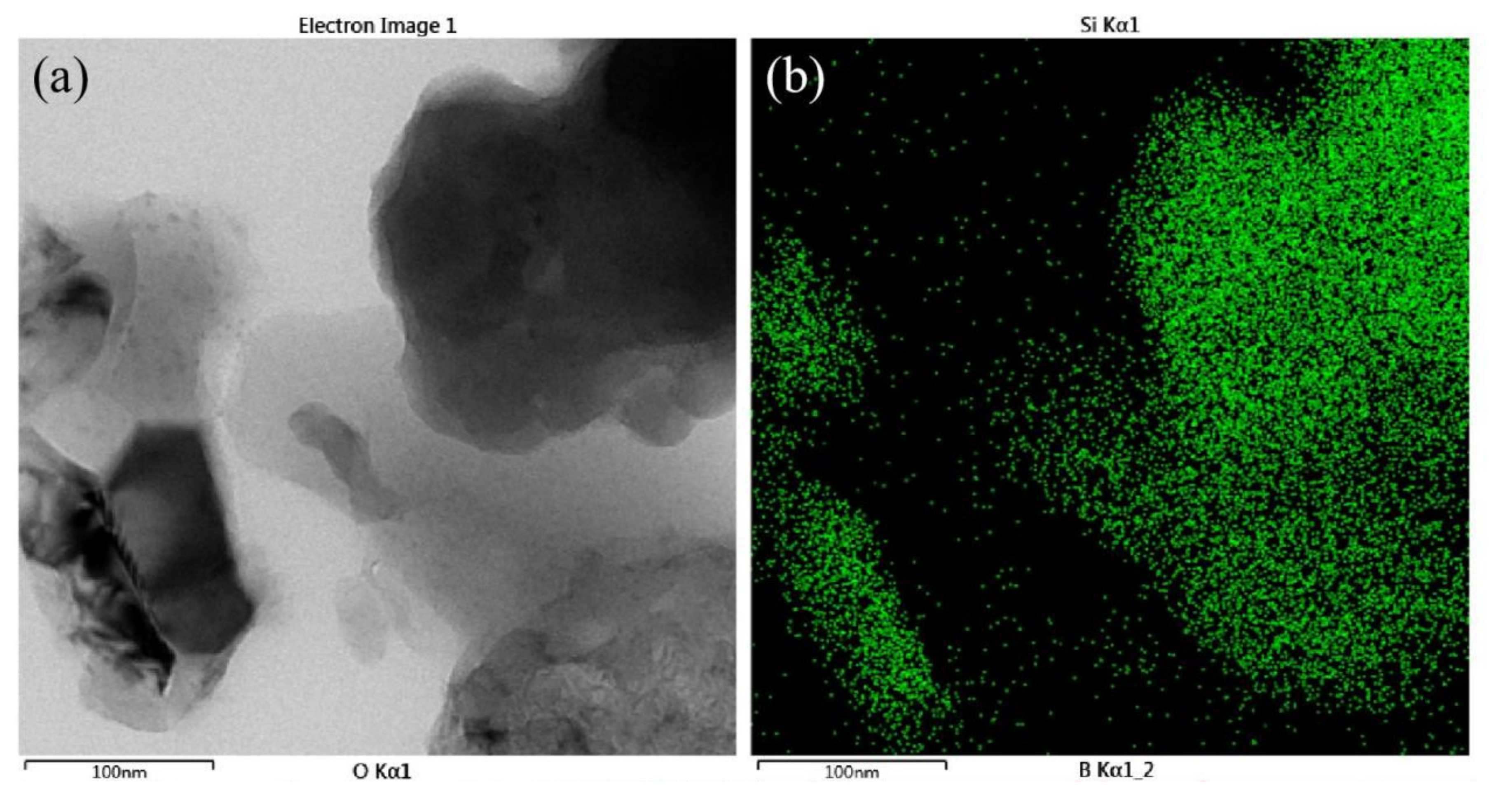
Figure 2 presents XRD and Raman spectra results. The component of the sample deposited at 1100 °C with B additives is mostly 3C-SiC. There are no impurity peaks in the sample spectra. The results show a standard 3C-SiC pattern, which conforms to the SAED result. Normally, 3C-SiC has a face-centered cubic structure. It is difficult for materials with cubic structures to form nanosheets. This material profits from the fusion and crystallization processes at the low temperature used. The fusion process can be interrupted by the B additives. Figure 2b shows the Raman spectra for the multi-layer SiC: the peaks at 793 cm−1 and 973 cm−1 are the TO and LO signals of the 3C-SiC; there are also B4C peaks at 478 cm−1 and 1087 cm−1. The Raman spectra show that there are B-C bonds in the multi-layer SiC, but B4C crystals have not formed, according to the XRD pattern in Figure 2a. The EDS mapping result for the SiC single layer is shown in Figure 3. Some regions of the SiC nanosheet oxidized after being peeled away from the multi-layer structure. The B elements and the O elements are distributed in different regions, indicating that the B elements can prevent the SiC from being oxidized, which means that the B elements and the B-C bonds are located at the surface of the single SiC layer. This explains why the nanosheets consist of 3C-SiC. The stability of the SiC nanosheets is protected by the B-C bonds on the surface. The results also show that the multi-layer structure offers an effective means of improving the oxidation resistance of SiC nanolayer structures.
We then studied the effects of the B additives on the CVD process. A SiC film annealed at 1800 °C is shown in Figure 4. The layers in the SiC separated after high-temperature annealing. The EDS mapping results in Figure 4b,c show that the B elements separated from the SiC. Boron is distributed among the SiC layers. This proves that the B stays between the SiC thin layers, and the multi-layer structure is formed because the B element aggregates spontaneously between the SiC layers during the deposition process. The formation mechanism of the deposition process is shown in Figure 4d. The SiC layer is formed through a fusion process at this temperature; the B elements float on the surface of the SiC and form B layers between the SiC layers, and the B-C bonds are formed between the SiC layers and B layers, the B-C bonds being responsible for the single SiC layer in the sample. Since the B-C bonds only form between the two different layers, there are no B4C crystals in the multi-layer SiC. This result conforms with the Raman spectra and with the XRD results and also explains why the multi-layer structure does not form with a large grain area. In addition, the SiC is separated into thin layers and atoms crystallize more easily in thin layers than in a large bulk.
As shown in Figure 4a, there are large and faceted grains in the SiC films after annealing. The SiC nanosheets are destroyed by the large grains. In this experiment, the formation of multi-layer structures in SiC is related to grain size. This also indicates that the B additives have a greater influence when the SiC film is formed through fusion and crystallization processes; B additives will only separate the poorly crystallized SiC but not the large SiC grains into layers. Since the well-crystallized SiC is less affected by the B elements, the SiC layers, as with graphene oxide, can only be fabricated at low deposition temperatures (below 1300 °C).
PL signals for the normal SiC films and for the multi-layer SiC films were taken to investigate the electronic properties of the 2D planes in SiC. The normal SiC films were also prepared through the CVD method using the parameters described in other articles [34]. Previous research on 2D materials has shown that there is a transition from an indirect bandgap to a direct bandgap in nanolayers which leads to photoluminescence emissions. As shown in Figure 5, there is a modulation in PL peak positions between multi-layer SiC and normal SiC. The peak position shifted significantly to the right after the SiC film was separated into a multi-layer structure. The difference may be due to the nanolayer structure in B-doped SiC, which shows the potential for the application of multi-layer SiC in electronics. Furthermore, the modulation of PL peaks could also be related to the B-C bonds and Si-O bonds in SiC nanolayers, all of which will be investigated in future work.
4. Conclusions
In this paper, new multi-layer-structured SiC films and SiC nanosheets were fabricated through the CVD method with B additives. The thicknesses of single nanosheets in the SiC films fabricated in this research were 8–10 nm. The experimental results showed that the nanosheets were pure SiC with B-C bonds on the surface. The B-C bonds on the surface of the SiC nanosheets and the multi-layer structure improved the oxidation resistance of the SiC nanolayers. The effect of the B additives on the CVD process were investigated: the crystallization and purity of the SiC films deposited at a low temperature (1100 °C) were promoted by the addition of B. Boron layers formed between the SiC nanolayers and separated the SiC films to give a multi-layer structure in the growth directions. The experimental results indicated that a multi-layer SiC film will only be prepared when there is no large SiC grain formed during the CVD process. The multi-layer SiC films show a different bandgap to normal SiC films. These results indicate that SiC has the potential to be applied in electronics.
Author Contributions
Conceptualization, R.L. and X.Y.; Investigation, X.Y.; data curation, R.L. and M.L.; resources, B.L.; writing—original draft preparation, X.Y..; writing—review and editing, R.L. and M.L. All authors have read and agreed to the published version of the manuscript.
Funding
This work was supported by the National S&T Major Project of China (2017ZX06901025).
Institutional Review Board Statement
Not applicable.
Informed Consent Statement
Not applicable.
Data Availability Statement
The data used in the study are available from the corresponding author upon reasonable request.
Conflicts of Interest
The authors declare that they have no competing interest.
References
- You, J.W.; Bongu, S.R.; Bao, Q.; Panoiu, N.C. Nonlinear optical properties and applications of 2D materials: Theoretical and experimental aspects. Nanophotonics 2019, 8, 63–97. [Google Scholar] [CrossRef]
- Zhuang, X.; Mai, Y.; Wu, D.; Zhang, F.; Feng, X. Two-dimensional soft nanomaterials: A fascinating world of materials. Adv. Mater. 2015, 27, 403–427. [Google Scholar] [CrossRef]
- Sun, Y.; Gao, S.; Lei, F.; Xiao, C.; Xie, Y. Ultrathin two-dimensional inorganic materials: New opportunities for solid state nanochemistry. Acc. Chem. Res. 2015, 48, 3–12. [Google Scholar] [CrossRef]
- Dubertret, B.; Heine, T.; Terrones, M. The rise of two-dimensional materials. Acc. Chem. Res. 2015, 48, 1–2. [Google Scholar] [CrossRef]
- Ahn, E.C. 2D materials for spintronic devices. npj 2D Mater. Appl. 2020, 4, 17. [Google Scholar] [CrossRef]
- Glavin, N.R.; Rao, R.; Varshney, V.; Bianco, E.; Apte, A.; Roy, A.; Ringe, E.; Ajayan, P.M. Emerging Applications of Elemental 2D Materials. Adv. Mater. 2020, 32, 1904302. [Google Scholar] [CrossRef]
- Zhang, Y.; Yao, Y.; Sendeku, M.G.; Yin, L.; Zhan, X.; Wang, F.; Wang, Z.; He, J. Recent Progress in CVD Growth of 2D Transition Metal Dichalcogenides and Related Heterostructures. Adv. Mater. 2019, 31, 1901694. [Google Scholar] [CrossRef]
- Molas, M.R.; Nogajewski, K.; Slobodeniuk, A.O.; Binder, J.; Bartos, M.; Potemski, M. The optical response of monolayer, few-layer and bulk tungsten disulfide. Nanoscale 2017, 9, 13128–13141. [Google Scholar] [CrossRef]
- Tongay, S.; Sahin, H.; Ko, C.; Luce, A.; Fan, W.; Liu, K.; Zhou, J.; Huang, Y.S.; Ho, C.H.; Yan, J.; et al. Monolayer behaviour in bulk ReS2 due to electronic and vibrational decoupling. Nat. Commun. 2014, 5, 3252. [Google Scholar] [CrossRef]
- Zhou, H.; Chen, Z.; Kountoupi, E.; Tsoukalou, A.; Abdala, P.M.; Florian, P.; Fedorov, A.; Muller, C.R. Two-dimensional molybdenum carbide 2D-Mo2C as a superior catalyst for CO2 hydrogenation. Nat. Commun. 2021, 12, 5510. [Google Scholar] [CrossRef]
- Qian, Q.; Lei, J.; Wei, J.; Zhang, Z.; Tang, G.; Zhong, K.; Zheng, Z.; Chen, K.J. 2D materials as semiconducting gate for field-effect transistors with inherent over-voltage protection and boosted ON-current. npj 2D Mater. Appl. 2019, 3, 24. [Google Scholar] [CrossRef]
- Dai, Z.; Liu, L.; Zhang, Z. Strain Engineering of 2D Materials: Issues and Opportunities at the Interface. Adv. Mater. 2019, 31, 1805417. [Google Scholar] [CrossRef]
- Kang, S.; Lee, D.; Kim, J.; Capasso, A.; Kang, H.S.; Park, J.-W.; Lee, C.-H.; Lee, G.-H. 2D semiconducting materials for electronic and optoelectronic applications: Potential and challenge. 2D Mater. 2020, 7, 022003. [Google Scholar] [CrossRef]
- Chaves, A.; Azadani, J.G.; Alsalman, H.; da Costa, D.R.; Frisenda, R.; Chaves, A.J.; Song, S.H.; Kim, Y.D.; He, D.; Zhou, J.; et al. Bandgap engineering of two-dimensional semiconductor materials. npj 2D Mater. Appl. 2020, 4, 1–12. [Google Scholar] [CrossRef]
- Guo, Y.; Liu, C.; Yin, Q.; Wei, C.; Lin, S.; Hoffman, T.B.; Zhao, Y.; Edgar, J.H.; Chen, Q.; Lau, S.P.; et al. Distinctive in-Plane Cleavage Behaviors of Two-Dimensional Layered Materials. ACS Nano 2016, 10, 8980–8988. [Google Scholar] [CrossRef]
- Osanloo, M.R.; Van de Put, M.L.; Saadat, A.; Vandenberghe, W.G. Identification of two-dimensional layered dielectrics from first principles. Nat. Commun. 2021, 12, 5051. [Google Scholar] [CrossRef]
- Shi, Z.; Zhang, Z.; Kutana, A.; Yakobson, B.I. Predicting Two-Dimensional Silicon Carbide Monolayers. ACS Nano 2015, 9, 9802–9809. [Google Scholar] [CrossRef]
- Lü, T.-Y.; Liao, X.-X.; Wang, H.-Q.; Zheng, J.-C. Tuning the indirect–direct band gap transition of SiC, GeC and SnC monolayer in a graphene-like honeycomb structure by strain engineering: A quasiparticle GW study. J. Mater. Chem. 2012, 22, 10062–10068. [Google Scholar] [CrossRef]
- Fan, D.; Lu, S.; Guo, Y.; Hu, X. Novel bonding patterns and optoelectronic properties of the two-dimensional SixCymonolayers. J. Mater. Chem. C 2017, 5, 3561–3567. [Google Scholar] [CrossRef]
- Chabi, S.; Kadel, K. Two-Dimensional Silicon Carbide: Emerging Direct Band Gap Semiconductor. Nanomaterials 2020, 10, 2226. [Google Scholar] [CrossRef]
- Belarouci, B.; Ouahrani, T.; Benabdallah, N.; Morales-García, A.; Belabbas, I. Two-dimensional silicon carbide structure under uniaxial strains, electronic and bonding analysis. Comput. Mater. Sci. 2018, 151, 288–295. [Google Scholar] [CrossRef]
- Zhang, H. Ultrathin Two-Dimensional Nanomaterials. ACS Nano 2015, 9, 9451–9469. [Google Scholar] [CrossRef]
- Lin, S.S. Light-Emitting Two-Dimensional Ultrathin Silicon Carbide. J. Phys. Chem. C 2012, 116, 3951–3955. [Google Scholar] [CrossRef]
- Chabi, S.; Guler, Z.; Brearley, A.J.; Benavidez, A.D.; Luk, T.S. The Creation of True Two-Dimensional Silicon Carbide. Nanomaterials 2021, 11, 1799. [Google Scholar] [CrossRef] [PubMed]
- Niu, L.; Coleman, J.N.; Zhang, H.; Shin, H.; Chhowalla, M.; Zheng, Z. Production of Two-Dimensional Nanomaterials via Liquid-Based Direct Exfoliation. Small 2016, 12, 272–293. [Google Scholar] [CrossRef]
- Yi, K.; Liu, D.; Chen, X.; Yang, J.; Wei, D.; Liu, Y.; Wei, D. Plasma-Enhanced Chemical Vapor Deposition of Two-Dimensional Materials for Applications. Acc. Chem. Res. 2021, 54, 1011–1022. [Google Scholar] [CrossRef]
- Gu, Y.; Cai, H.; Dong, J.; Yu, Y.; Hoffman, A.N.; Liu, C.; Oyedele, A.D.; Lin, Y.C.; Ge, Z.; Puretzky, A.A.; et al. Two-Dimensional Palladium Diselenide with Strong In-Plane Optical Anisotropy and High Mobility Grown by Chemical Vapor Deposition. Adv. Mater. 2020, 32, 1906238. [Google Scholar] [CrossRef]
- Wang, C.; Huang, N.; Zhuang, H.; Zhai, Z.; Yang, B.; Liu, L.; Jiang, X. Growth of large-scale heteroepitaxial 3C-SiC films and nanosheets on silicon substrates by microwave plasma enhanced CVD at higher powers. Surf. Coat. Technol. 2016, 299, 96–103. [Google Scholar] [CrossRef]
- Xu, Q.; Tu, R.; Sun, Q.; Yang, M.; Li, Q.; Zhang, S.; Zhang, L.; Goto, T.; Ohmori, H.; Shi, J.; et al. Morphology controlling of 〈111〉-3C–SiC films by HMDS flow rate in LCVD. RSC Adv. 2019, 9, 2426–2430. [Google Scholar] [CrossRef]
- Guilhon, I.; Teles, L.K.; Marques, M.; Pela, R.R.; Bechstedt, F. Influence of structure and thermodynamic stability on electronic properties of two-dimensional SiC, SiGe, and GeC alloys. Phys. Rev. B 2015, 92, 075435. [Google Scholar] [CrossRef]
- Xu, S.G.; Li, X.T.; Zhao, Y.J.; Liao, J.H.; Xu, W.P.; Yang, X.B.; Xu, H. Two-Dimensional Semiconducting Boron Monolayers. J. Am. Chem. Soc. 2017, 139, 17233–17236. [Google Scholar] [CrossRef]
- Wu, X.J.; Dai, J.; Zhao, Y.; Zhuo, Z.W.; Yang, J.L.; Zeng, X.C. Two-Dimensional Boron Monolayer Sheets. ACS Nano 2012, 6, 7443–7453. [Google Scholar] [CrossRef]
- Yang, X.; Zhang, F.; You, Y.; Guo, M.; Zhong, Y.; Wang, P.; Lin, J.; Zhu, Z.; Zhu, L. Growth process and mechanism of SiC layer deposited by CVD method at normal atmosphere. J. Eur. Ceram. Soc. 2019, 39, 4495–4500. [Google Scholar] [CrossRef]
- Liu, R.; Liu, M.; Chang, J. Experimental phase diagram of SiC in CH3SiCl3–Ar–H2 system produced by fluidized bed chemical vapor deposition and its nuclear applications. J. Mater. Res. 2016, 31, 2695–2705. [Google Scholar] [CrossRef]
Figure 1.
(a) Fabrication process of the SiC nanosheets. (b) SEM image of the cross section. (c) TEM image of the single SiC nanosheet. (d) TEM image of the single SiC nanosheet. (e) SAED result for the SiC nanosheet.
Figure 1.
(a) Fabrication process of the SiC nanosheets. (b) SEM image of the cross section. (c) TEM image of the single SiC nanosheet. (d) TEM image of the single SiC nanosheet. (e) SAED result for the SiC nanosheet.

Figure 2.
(a) XRD pattern for the multi-layer SiC. (b) Raman spectra for the multi-layer SiC.

Figure 3.
(a) The original TEM image. (b) Distribution of Si elements. (c) Distribution of O elements. (d) Distribution of B elements.
Figure 3.
(a) The original TEM image. (b) Distribution of Si elements. (c) Distribution of O elements. (d) Distribution of B elements.


Figure 4.
(a) SEM image of the SiC annealed at 1800 °C. (b) EDS mapping result for the Si. (c) EDS mapping result for the B. (d) Growth process of the multi-layer SiC.
Figure 4.
(a) SEM image of the SiC annealed at 1800 °C. (b) EDS mapping result for the Si. (c) EDS mapping result for the B. (d) Growth process of the multi-layer SiC.

Figure 5.
PL signals for different SiC films. (a) Normal SiC film. (b) Multi-layer SiC film.

Publisher’s Note: MDPI stays neutral with regard to jurisdictional claims in published maps and institutional affiliations. |
© 2022 by the authors. Licensee MDPI, Basel, Switzerland. This article is an open access article distributed under the terms and conditions of the Creative Commons Attribution (CC BY) license (https://creativecommons.org/licenses/by/4.0/).
Share and Cite
MDPI and ACS Style
Yang, X.; Liu, R.; Liu, B.; Liu, M. Synthesis of Ultra-Thin Two-Dimensional SiC Using the CVD Method. Energies 2022, 15, 6351. https://0-doi-org.brum.beds.ac.uk/10.3390/en15176351
AMA Style
Yang X, Liu R, Liu B, Liu M. Synthesis of Ultra-Thin Two-Dimensional SiC Using the CVD Method. Energies. 2022; 15(17):6351. https://0-doi-org.brum.beds.ac.uk/10.3390/en15176351
Chicago/Turabian StyleYang, Xu, Rongzheng Liu, Bing Liu, and Malin Liu. 2022. "Synthesis of Ultra-Thin Two-Dimensional SiC Using the CVD Method" Energies 15, no. 17: 6351. https://0-doi-org.brum.beds.ac.uk/10.3390/en15176351
Note that from the first issue of 2016, this journal uses article numbers instead of page numbers. See further details here.