
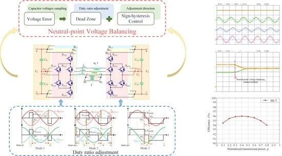
Neutral-Point Voltage Balancing Method for Three-Phase Three-Level Dual-Active-Bridge Converters


The State Key Laboratory of Advanced Electromagnetic Engineering and Technology, School of Electrical and Electronic Engineering, Huazhong University of Science and Technology, Wuhan 430074, China
*
Author to whom correspondence should be addressed.
Energies 2022, 15(17), 6463; https://0-doi-org.brum.beds.ac.uk/10.3390/en15176463
Submission received: 10 August 2022
/
Revised: 31 August 2022
/
Accepted: 1 September 2022
/
Published: 4 September 2022
(This article belongs to the Special Issue Modeling, Control and Design of Power Electronics Converters)
Abstract
:Three-phase three-level dual-active-bridge (3L-DAB3) converters are a potential topology for high-voltage and high-power applications. Neutral-point voltage balancing is a complex and important issue for three-level (3L) circuits. Compared with the single-phase 3L dual-active-bridge converter, the self-balancing capability of the 3L-DAB3 is limited. To guarantee the reliability of the converter, a neutral-point voltage balancing method for the 3L-DAB3 is proposed in this paper. First, the neutral-point voltage balancing principle of the 3L-DAB3 is analyzed. Then, the relationship between the duty ratio adjustment and injected neutral-point charge is described. In order to guarantee accurate neutral-point voltage balance, the proposed balancing method adopts a sign-hysteresis control with a dead zone. The dead zone is responsible for whether the duty ratio adjustment is activated, and the sign-hysteresis control guarantees a correct adjustment direction. The proposed neutral-point voltage balancing method only needs to sample the capacitor voltages, thus avoiding a complex parameter design and making it easy to implement. The transmission power of the converter is not affected during the adjustment process. The proposed balancing method has a rapid response speed and does not have problems with respect to stability. Finally, experiments were conducted on a 3.6 kW laboratory prototype. The validity and performance of the proposed neutral-point voltage balancing method were verified on the basis of the simulation and experimental results.
1. Introduction
Isolated DC–DC converters have been widely used in high-power applications, such as solid-state transformers, hybrid electric vehicles, energy storage systems and DC distribution systems [1,2,3,4,5]. Most of these applications require a bidirectional power flow, a high efficiency, and a high-power density. As a promising isolated DC–DC converter topology, the dual-active-bridge (DAB) converter has been extensively used in recent years due to its easy realization of soft-switching, electrical isolation, and its modular and symmetric structure [6,7,8].
Compared with the conventional single-phase DAB (DAB1), the three-phase DAB (DAB3), first proposed in [9], exhibits advantages of a reduced filter volume, a higher efficiency, and a higher power density [10,11,12,13,14,15]. Therefore, the DAB3 is suitable for high-power applications. Phase shift control is the most common modulation strategy for the two-level DAB3. Under symmetric modulation, the duty ratios of the two bridges are fixed at 50%, and the phase shift between the primary and secondary sides is the only control degree of freedom. However, it is easy to lose zero-voltage switching (ZVS) at light-load or non-unity voltage ratios. To extend the ZVS range and improve the light-load efficiency, many optimization strategies have been proposed, such as negative-sequence modulation [16], asymmetrical duty-cycle control [17,18], single-phase operation [19], and simultaneous pulse-width modulation control [20].
Introducing three-level (3L) circuits into the DAB3 is a possible way of improving their performance. The three-phase three-level DAB (3L-DAB3) converter, introduced in [21,22], is able to provide a wide ZVS range with symmetrical voltage and current waveforms, and has three control degrees of freedom for the optimization of its performance [23,24]. Additionally, the 3L-DAB3 makes it possible to use lower voltage-rated power devices with better performance features, and reduces switching and conduction losses [25].
The neutral-point voltage balancing of 3L circuits is a complex and important issue [26,27]. The offset of neutral-point voltage leads to overvoltage on a portion of the switches, which affects the reliability of the converter. The 3L half-bridge DAB1 (3LHB-DAB1) has a strong neutral-point voltage self-balancing capability, and thus the neutral-point voltage balancing algorithm is not required. In the 3L full-bridge DAB1 (3LFB-DAB1), neutral-point voltage balancing can be realized by introducing an additional LC branch [28], alternately using complementary switching modes [29], or adjusting the duty ratio of the switching state [30,31].
However, the 3L-DAB3 cannot be regarded as a simple superposition of three 3LHB-DAB1. It has a specific neutral-point voltage balancing principle, which is different from that of the DAB1. The existing neutral-point voltage balancing methods for the DAB1 cannot be directly applied. An active neutral-point voltage control was discussed for the 3L-DAB3 in bipolar operation in [32], but the lookup tables that were used are complicated. The active control lacks the necessary theoretical analysis of the neutral-point voltage balancing principle of the 3L-DAB3. Moreover, it is only applicable in a specific operating mode, with all operating modes of the converter not having been verified. To date, the theoretical analysis of the neutral-point voltage offset and the balancing principle of the 3L-DAB3 have not been described in the existing research. Therefore, a practical neutral-point voltage balancing method for all 3L-DAB3 operating conditions is needed.
This paper focuses on the neutral-point voltage balancing principle and proposes a neutral-point voltage balancing method for the 3L-DAB3. First, the effective charging intervals of neutral points are indicated in all operating modes. The inner duty ratio is the main factor of the charging intervals, and it can be modulated. Then, with the adjustment of the duty ratio, it is possible to derive the introduced neutral-point charge. The relationship between the sign of the duty ratio adjustment and the sign of the introduced neutral-point charge is clear, and it provides theoretical support for the design of the hysteresis control. The sign-hysteresis control can be used to guarantee that the correct direction of adjustment is employed, and a dead zone is additionally applied to control the neutral-point voltage to within the region close to the balanced value, avoiding changes in the duty ratio during each switching period. Finally, the neutral-point voltage balancing method, consisting of the sign-hysteresis control with a dead zone, is obtained to maintain the neutral-point voltage balancing of the 3L-DAB3. More importantly, the theoretical analysis and proposed method of the neutral-point voltage balancing is applicable to all 3L-DAB3.
The rest of this paper is organized as follows. In Section 2, the topology and operating principle of the 3L-DAB3 are introduced. In Section 3, the neutral-point voltage balancing principle is presented. In Section 4, the control principle of the neutral-point voltage balancing is described, and a balancing method consisting of a sign-hysteresis control with a dead zone is proposed. Simulation and experimental verifications, performed using a 3.6 kW laboratory prototype, are provided in Section 5, and conclusions are drawn in Section 6.
2. Topology and Operating Principle of the 3L-DAB3
2.1. Topology of the 3L-DAB3
The circuit schematic of the 3L-DAB3 was introduced in [21,22]. Figure 1 shows the circuit schematic of the 3L-DAB3 that is discussed in this paper, in which two three-phase active neutral-point-clamped (ANPC) bridges are connected by a three-phase high-frequency transformer. According to the winding configuration of the three-phase transformer, the 3L-DAB3 has four magnetic structure types, with Y-Y, Y-∆, ∆-Y, and ∆-∆ configurations. Compared with the other types, the Y-Y winding configuration is able to effectively reduce the unbalanced phase current of the three-phase transformer and prevent high circulating currents under no-load conditions [33]. Therefore, in this paper, a 3L-DAB3 with a Y-Y winding configuration is discussed.
The three 3L ANPC bridges on the primary side are denoted as BA1, BB1, and BC1, and the three bridges on the secondary side are denoted as BA2, BB2, and BC2. The six switches of the 3L ANPC bridges are denoted as Sij1–Sij6, where the subscript i (i = A, B, C) represents the phases A, B, and C, and the subscript j (j = 1, 2) represents the primary side and the secondary side, respectively. The output terminals of the three-phase 3L ANPC bridges are denoted as Aj, Bj, and Cj, respectively. The VP and VS are the DC voltages. The CP1, CP2, CS1, and CS2 are the filter capacitors on the DC side, and the capacitor voltages are vCP1, vCP2, vCS2, and vCS2 and satisfy the constraints vCP1 + vCP2 = VP and vCS1 + vCS2 = VS. The equivalent inductor Li includes the transformer leakage inductor and the external series inductor. The phase current that flows through Li is denoted as iLi, and the terminal voltages of Li are denoted as vLij. The three-phase high-frequency transformer T has a turns-ratio of nk:1, and thus the voltage conversion ratio k of the converter is expressed as nkVS/VP. The voltage drop across Li is denoted as vLi and is equal to vLi1 − nkvLi2. The neutral points of two active bridges and the Y-Y winding are O1 and O2 and m1 and m2, respectively.
The equivalent circuit of the 3L-DAB3 is presented in Figure 2. The active bridges are equivalent to step-wave AC voltage sources with a Y configuration, connected through the series inductors. In the 3L-DAB3, the three 3L ANPC bridges on each side are modulated with a phase shift of 2π/3. Under the assumption that the parameters of each phase are symmetric, phase A is taken as an example for analysis in this paper.
2.2. Operating Principle of the 3L-DAB3
Each 3L ANPC bridge can output three voltage levels, Vdc/2, 0, and −Vdc/2 (Vdc is the DC-bus voltage), denoted as the P, O, and N states, respectively. The switching strategy for 3L ANPC bridges that is proposed in [34] is used in this paper to improve the performance.
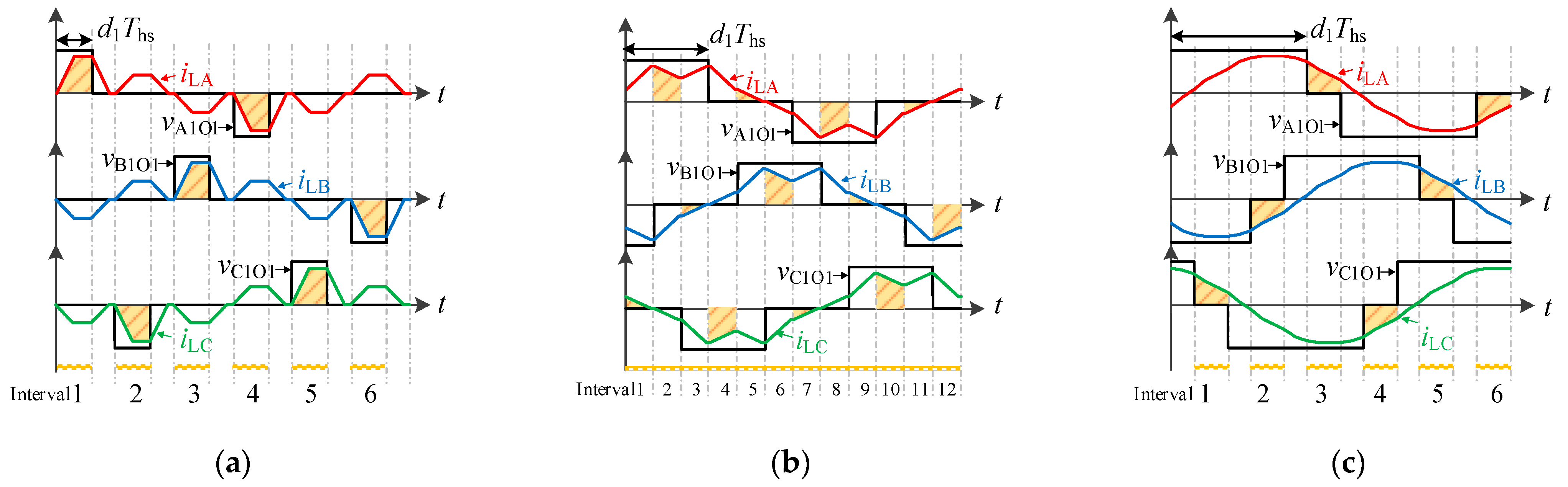
In Figure 3a, the durations of the P and N states in vi1O1 are the same, and they are modulated as d1Ths. d1 is the inner duty ratio of the primary side and satisfies the constraint 0 ≤ d1 ≤ 1. Ths is half of the switching period, and Ts is the switching period. The switching frequency is denoted as fs, and ω is the angular frequency. The vLA1 is obtained, and has one control degree of freedom, d1. On the secondary side, the vLA2 can be generated in the same way, with one control degree of freedom, d2, which is the inner duty ratio of the secondary side and satisfies the constraint 0 ≤ d2 ≤ 1. For the power transmission of the 3L-DAB3, the outer duty ratio d is added into the modulation to form a phase shift between vLA1 and vLA2, as shown in Figure 3b.
The vm1O1 and vm2O2 are the neutral-point voltages of m1 and m2 and they refer to O1 and O2, respectively [35], which are given by (1). The vAjOj, vBjOj, and vCjOj are the AC side voltages of the 3L ANPC bridge BAj, BBj, and BCj refer to Oj, respectively. The primary and secondary terminal voltages vLij of the inductor Li are expressed by (2).
It can be observed that the AC-side voltages of the 3L ANPC bridges are coupled under the Y-Y winding configuration. According to the ranges of dj, vmjOj has three operating modes, as shown in Figure 4.
- (1)
- Mode 1: The inner duty ratio dj satisfies the constraint 0 ≤ dj ≤ 1/3. The durations of the P and N states in vmjOj are the same, and they are controlled as djThs; the voltage levels and steps of vLAj are illustrated in Figure 4a.
- (2)
- Mode 2: The inner duty ratio dj satisfies the constraint 1/3 < dj ≤ 2/3. The durations of the P and N states in vmjOj are the same, and they are controlled as (2/3 − dj)Ths; the voltage levels and steps of vLAj are illustrated in Figure 4b.
- (3)
- Mode 3: The inner duty ratio dj satisfies the constraint 2/3 < dj ≤ 1. The durations of the P and N states in vmjOj are the same, and they are controlled as (dj − 2/3)Ths; the voltage levels and steps of vLAj are illustrated in Figure 4c.
According to Figure 3 and Figure 4, the time-domain analysis is complex in 3L-DAB3 due to the large number of voltage levels and steps. However, the phase voltages and currents are near sinusoidal in the 3L-DAB3, which makes it suitable for analysis on the basis of the fundamental harmonic approximation (FHA) method [36]. The vA1O1 presents the odd and half-wave symmetry, and these can be transformed into (3) on the basis of the Fourier series, where the odd harmonic number n satisfies n = 1, 3, 5, 7, …
According to (2), vLA1 can be obtained and expressed by (4). Considering that the 3nth harmonic is eliminated under the Y-Y winding configuration, the odd harmonic number n satisfies n = 1, 5, 7, 11, … in (4). Similarly, vLA2 is expressed by (5).
The phase current iLA in Figure 3b can be calculated using (6), where λ denotes the time within a switching period. Due to the half-wave symmetry, iLA(0) can be calculated. Then, substituting iLA(0) into (6), the phase current iLA is obtained, which can be expressed as shown in (7).
Only taking the fundamental component (n = 1) into account, the fundamental component vA1O1,1 can be expressed as in (8), and iLA,1 can be derived using (9).
3. Neutral-Point Voltage Balancing Principle
The neutral-point voltage is affected by the flow direction of the neutral-point instantaneous current iNPj. The current that is being drawn from the neutral point is defined as iNPj > 0, which is discharged at the neutral point Oj. Thus, the neutral-point potential decreases. Otherwise, iNPj charges the neutral point Oj, and the neutral-point potential increases when iNPj < 0. Therefore, the neutral-point average current INPj reflects the total charge that is injected into or drawn from the neutral point Oj in a given switching period. In order to maintain the neutral-point voltage balance, it is necessary to guarantee INPj = 0 within a switching period.
3.1. Neutral-Point Voltage Self-Balancing of the 3LHB-DAB1
The current paths under the P and N states for the 3LHB-DAB1 are shown in Figure 5. The phase current that is drawn from the output terminal A1 is defined as iLA > 0. Since iLA flows directly back to the neutral point O1 through the primary winding of the transformer, iNP1 = −iLA. The neutral point instantaneous current iNP1 in the 3L-DAB3 can be expressed as shown in (12), where dm is the duration ratio of the P or N state, and the subscript m (m = P, N) represents the P and N states, respectively. Under normal operation, the durations of the P and N states are equal, and therefore dP = dN. With the half-wave symmetry of iLA, INP1 = 0. The neutral-point voltage remains balanced.
Assuming that vCP2 is lower than Vdc/2, the forward DC bias is generated in the primary winding of the transformer and the current iLA. According to (12), INP1 < 0. Since iLA flows directly back to the O1 in the 3LHB-DAB1, the neutral point is charged directly and increases back to the balanced value, eliminating the forward DC bias. Therefore, the 3LHB-DAB1 has a strong neutral-point voltage self-balancing capability.
However, the 3L-DAB3 cannot be seen as a simple superposition of three 3LHB-DAB1, and neutral-point voltage balancing cannot be treated in the same way. Under the Y-Y winding configuration, iLi does not flow directly back to the neutral point Oj, as shown in Figure 1. It is difficult to maintain neutral-point voltage self-balancing. Therefore, it is necessary to analyze the neutral-point balancing principle and propose a neutral-point voltage balancing method for the 3L-DAB3. The neutral point O1 of the primary side is taken as an example that will be analyzed in the following sections.
3.2. Neutral-Point Balancing Principle of the 3L-DAB3
Similar to the 3L three-phase inverter [37], the neutral-point instantaneous current iNP1 in the 3L-DAB3 can be expressed as shown in (13). Unless any one or two of the vi1O1 output the O state, the corresponding current iLi will not affect the neutral point O1. The vm1O1 has three operating modes, so iNP1 also has three charging and discharging modes, as shown in Figure 6.
The neutral-point current charging and discharging principles for the different modes can be described as follows:
- (1)
- Mode 1: When one bridge outputs the P or N state, iLi charges the neutral point O1 in the six yellow operating intervals, as shown in the shaded areas in Figure 6a. In these six intervals, iNP1 = −iLi. In the other six intervals, three 3L ANPC bridges output the O states and iNP1 = iLA + iLB + iLC = 0, which does not charge the neutral point O1. As an example, the current paths in Interval 1 of phase A are shown in Figure 7a.
- (2)
- Mode 2: The iNP1 in 12 operating intervals charges the neutral point O1, as shown in the shaded areas in Figure 6b. Generally, there are two different cases: in Intervals 2, 4, 6, 8, 10, and 12, iNP1 = −iLi; in Intervals 1, 3, 5, 7, 9, and 11, iNP1 = iLi. As an example, the current paths in Interval 8 of phase A are shown in Figure 7b.
- (3)
- Mode 3: When one bridge outputs the O state, iNP1 charges the neutral point O1 in the six yellow operating intervals, as shown in the shaded areas in Figure 6c. In these six intervals, iNP1 = iLi. In the other six intervals, three 3L ANPC bridges output the P or N states, iNP1 = 0, which does not charge the neutral point O1. As an example, the current paths in Interval 3 of phase A are shown are Figure 7c.
Figure 7.
Current path diagram of the neutral-point current charging and discharging intervals. (a) Interval 1 of Mode 1; (b) Interval 8 of Mode 2; (c) Interval 3 of Mode 3.
Figure 7.
Current path diagram of the neutral-point current charging and discharging intervals. (a) Interval 1 of Mode 1; (b) Interval 8 of Mode 2; (c) Interval 3 of Mode 3.

In Mode 1, assuming that vCP2 is lower than Vdc/2, the neutral-point charge generated by iLA in Intervals 1 and 4 is positive within a switching period, and it is same as that of the bridges BB1 and BC1. Therefore, the total charge that is injected into the neutral point O1 is positive, and therefore it charges the O1. The vCP2 increases to close to Vdc/2, and the neutral-point voltage tends to be self-balancing. In other operating modes, the self-balancing of the 3L-DAB3 is also valid, using the same means of analysis. The simulation waveforms of the capacitor voltages are illustrated in Figure 8. The neutral-point voltages of both sides exhibit this self-balancing trend, as shown in Figure 8a. However, the voltage oscillations over a long time are not acceptable, and they would lead to damage to the 3L-DAB3.
In practical systems, there are several factors that may affect neutral-point voltage balancing, such as asymmetric hardware parameters, and small differences in driving circuits and power devices, which cannot be avoided. On the other hand, the actual drive waveforms of switches include the dead time. Therefore, even if the dead time is considered, the charging intervals of the neutral points remain symmetric. The total neutral-point charge is zero within a switching period. The dead time of the switches does not affect the neutral-point voltage balancing or its control principle for the 3L-DAB3. Combined with the above analysis, when the durations of the P and N states are unequal, INPj ≠ 0, the neutral-point voltages will deviate from the balanced voltages, as shown in Figure 8b. Permanent neutral-point voltage imbalance would occur in such scenarios and it could even result in power devices in the converter being destroyed. Therefore, it is necessary to propose a neutral-point voltage balancing method that guarantees the reliability of the 3L-DAB3.
4. Neutral-Point Voltage Balancing Method
4.1. Control Principle of the Neutral-Point Voltage Balancing Method
When the offset of the neutral-point voltage appears, one intuitive method for restoring balance is to adjust the duty ratio while not introducing a DC bias into the transformer. That is, when a voltage imbalance appears, the inner duty ratio dj should be modified to dj + Δdj, introducing a nonzero charge ΔQNPj, injected into or drawn from the neutral point Oj. The duty ratio Δdj is usually taken as −0.04~0.04, which is small, and thus does not affect the transmission power [27].
As can be seen from (9), the fundamental component of phase current iLi,1 can be regarded as a function of three control degrees of freedom (d, d1, and d2), and the voltage conversion ratio k, and iLi,1 can be expressed as shown in (14). Neutral-point voltage balancing can be achieved by regulating the charge that is injected into the neutral point by means of the duty ratio adjustment, and the introduced charge ΔQNPj can be derived using (15), where tc is the efficient charging time under the duty ratio adjustment.
ΔQNPj is related to the operating conditions, which determine the voltage conversion ratio k and the three control degrees of freedom under basic modulation. The control parameter design needs to derive the relationship between Δdj and ΔQNPj. According to Figure 6, the efficient time tc can be easily deduced using the duty ratio adjustment, but ΔQNPj also depends on different operating conditions. Therefore, it is difficult to obtain the exact direction and quantity of ΔQNPj using (15), and the parameter design of the balancing control is complex.
A neutral-point voltage balancing method is proposed below, that consists of a sign-hysteresis control with a dead zone. Although the exact value of ΔQNPj with the specific Δdj is hard to calculate, the following analysis shows that the sign of ΔQNPj can change inversely with changes in the sign of Δdj. This provides the theoretical basis for the sign-hysteresis design. Furthermore, in order to avoid changes in the duty ratio during each switching period, a dead zone can be set. The neutral-point voltage is adjusted by a small change during a switching period that does not affect the normal modulation or transmission power of the converter. The proposed neutral-point voltage balancing method only needs to sample the capacitor voltages, and has a rapid response speed, without being subject to stability problems. In contrast to the methods that are described in previous work, this proposed method is applicable in all operating modes of the 3L-DAB3. The complexity of the control parameter design is avoided, making it easy to implement. The following derivation takes phase A as an example.
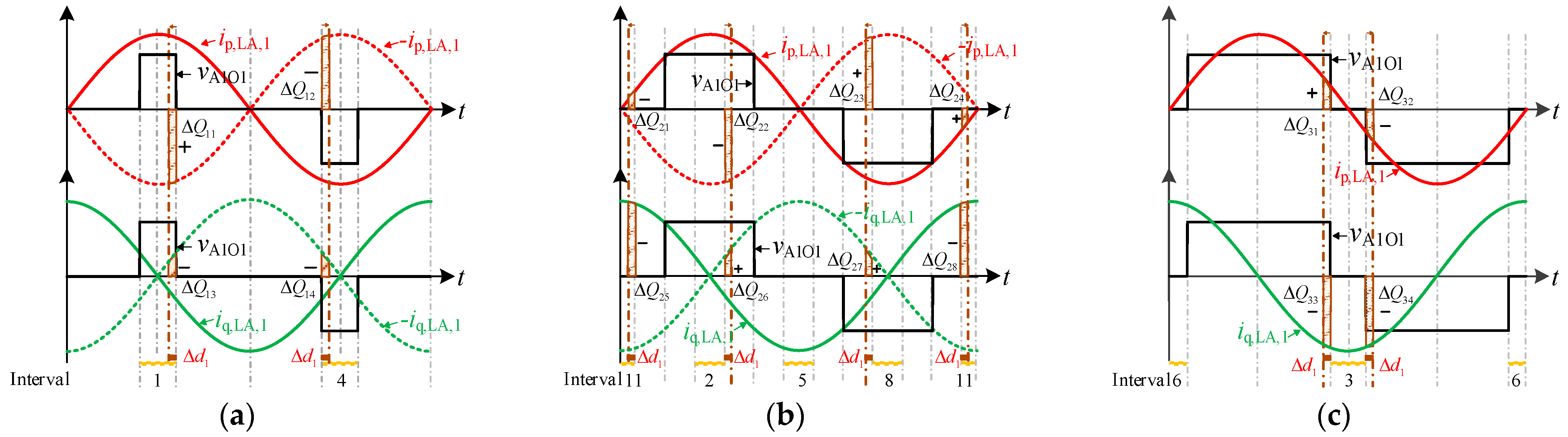
First, iLA,1 can be decoupled into the component ip,LA,1, which is in phase with vA1O1,1, and the component iq,LA,1, which is in quadrature with vA1O1,1. The iLA,1 can be expressed as shown in (16), where Ip,LA,1 and Iq,LA,1 are the average currents of ip,LA,1 and iq,LA,1 in a switching period, respectively.
The relationship between ip,LA,1, iq,LA,1, and vA1O1 is shown in Figure 9. On the basis of (13) and Figure 6, it is possible to obtain the neutral-point charge in each interval of phase A. The yellow shaded areas in Figure 9 represent the charge that is injected into (charging area ‘+’) or drawn from (discharging area ‘−’) the neutral point O1 by iLA,1. Due to the odd and half-wave symmetry of vA1O1, the total charge that is injected into O1 of phase A is zero in a switching period. The neutral-point voltage maintains balanced.
When small perturbations in the neutral-point voltage appear, a duty ratio adjustment should be performed to introduce a nonzero charge ΔQz to balance the neutral-point voltage. The changes in the operating intervals (brown, dotted lines) and introduced charge ΔQzn (brown striped areas) are depicted in Figure 10, in which the inner duty ratio of vA1O1 is adjusted to d1 + Δd1 (Δd1 < 0). The total charge ΔQz is the sum of ΔQzn, where the subscript z (z = 1, 2, 3) represents operating modes 1, 2, and 3, and the subscript n represents different parts of the charge, respectively.
In Mode 2, ip,LA,1 does not change the total charge that is injected into the neutral-point before and after the duty ratio adjustment. As shown in Figure 10b, the introduced charge ΔQ21 = −ΔQ24 and ΔQ22 = −ΔQ23, and the sum of them is zero due to the odd and half-wave symmetry of vA1O1 and ip,LA,1. For iq,LA,1, ΔQ26 and ΔQ27 are positive, and ΔQ25 and ΔQ28 are negative. The total introduced charge ΔQ2 is negative in a switching period. Similarly, the total introduced charge ΔQ1 in Mode 1 and ΔQ3 in Mode 3 are negative, too. When Δd1 > 0, the total introduced charge ΔQz will be positive in a switching period, which is the opposite of Δd1 < 0. The sign of ΔQz changes inversely with the change in the sign of Δd1.
4.2. Realization of the Proposed Balancing Method
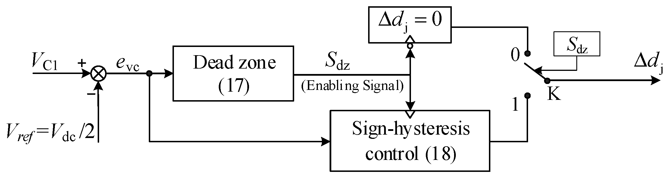
When a large perturbation of the neutral-point voltage appears, the voltages and currents will deviate greatly from the balanced value, and the control principle that is discussed above may not be valid. However, the sign of the ΔQNPj still changes inversely with the change in the sign of Δdj. Therefore, a sign-hysteresis band can be used to regulate the sign of Δdj in such a scenario, and a dead zone can be set to decide whether to implement the duty ratio adjustment. The dead zone controls the neutral-point voltage to a value that is close to the balanced value, thus avoiding duty ratio changes in each switching period. Finally, a neutral-point voltage balancing method consisting of a sign-hysteresis control with a dead zone is proposed, as shown in Figure 11.
On the basis of the sampled capacitor voltage vCP1 and vCS1 and the reference voltage Vref, the determination as to whether to implement Δdj can be made. Vref is the reference value of the neutral-point voltage and is expressed as Vref = Vdc/2. The dead zone (Vref − hd, Vref + hd) is set to implement Δdj, and the dead zone characteristic DZ(∙) can be described as shown in (17), where evc is the voltage error and is expressed as evc = VC1 − Vref. Sdz is the enabling signal of the duty ratio adjustment. When Sdz = 0, the duty ratio adjustment is not implemented and Δdj = 0. When Sdz = 1, the initial Δdj is set, and the sign-hysteresis control is activated. In order to guarantee the accurate sign of Δdj, a sign-hysteresis band (Vref − H, Vref + H) is set, and the sign-hysteresis characteristic H(∙) is described as shown in (18).
The output Δdj of the neutral-point voltage balancing method is selected by the enabling the switch K, as shown in Figure 11. When Sdz = 0, K switches to Point 0, and Δdj = 0. When Sdz = 1, K switches to Point 1, and Δdj is determined by the sign-hysteresis control.
Furthermore, the phase current iLi has opposite effects on the neutral points of both sides. When iLi flows out of the neutral point O1, it flows relatively to the neutral point O2. Therefore, the duty ratio adjustment of the two sides should satisfy the constraint Δd2 = −Δd1 [38]. On the basis of the above analysis, it can be seen that hd is related to the ripple requirement of the capacitor voltages in steady state, and H can be set according to the maximum allowable ripple that satisfies the operating requirements of the 3L-DAB3. The proposed balancing method only needs to sample capacitor voltages and has a simple, logical judgement mechanism. The control algorithm and design are simple and easy to implement. Compared with the conventional algorithm, the complexity of the control parameter design is avoided, and there are no problems with respect to stability. The theoretical analysis method of the neutral-point voltage balancing principle is applicable to all 3L-DAB3, and the proposed balancing method can also be used in all 3L-DAB3.
5. Simulation Results and Experimental Verification
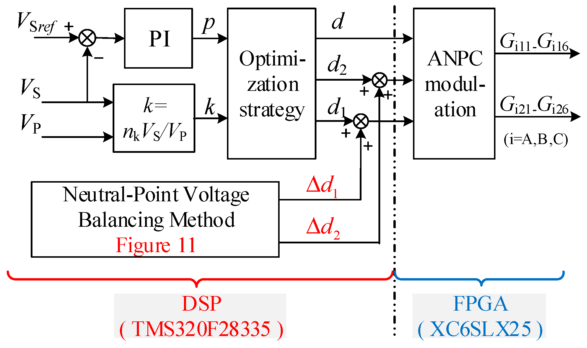
In this section, the simulation and experimental results are presented, verifying the effectiveness of the proposed balancing method. The experiments were conducted on a laboratory prototype of the 3L-DAB3 with the parameters that are listed in Table 1. Using the optimization strategies that are proposed in [34,36] and the closed-loop control that is proposed in [39], a digital controller, shown in Figure 12, was implemented using a TMS320F28335 DSP from TI and a Spartan6XC6SLX25 FPGA from Xilinx. p denotes the normalized power with a value of Pbase = 3nkVPVS/(π3fsLi), and VSref is the reference voltage of the secondary side. Gij1–Gij6 are the drive waveforms of the switches on the primary and secondary sides, respectively. The laboratory prototype is presented in Figure 13.
5.1. Simulation Results
The 3L-DAB3 with the proposed neutral-point voltage balancing method was simulated using MATLAB/Simulink software. A 3.6 kW 3L-DAB3 with the parameters that are listed in Table 1 was established to verify the performance of the proposed method.
The converter operates with an output voltage reference VSref = 300 V. The steady-state waveforms are illustrated in Figure 14. When the reference transmission power was set as 900 W, the resistance load was set to 100 Ω; the operating waveforms are presented in Figure 14a. The terminal voltage vLA1 operated in Mode 2 and vLA2 operated in Mode 3 with the neutral-point voltage balancing. When the reference transmission power was set at the rated power of 3.6 kW, the resistance load was set to 25 Ω; the operating waveforms are presented in Figure 14b. The vLA1 and vLA2 operated in Mode 3, and the phase current iLA became more sinusoidal with increasing transmission power. As shown in Figure 14c, with the close-loop control, the neutral-point voltage maintained balanced, and the output voltage responded quickly. The output voltage VS = 300 V, and the capacitor voltages vCP1 = vCP2 = 200 V and vCS1 = vCS2 = 150 V in the steady state. The FFT analysis results of the system are presented in Figure 15. With the applied filter capacitor CS1 = CS2 = 150 μF, the THD results of the system were controlled to 0.04% and 0.02% under 900 W and 3.6 kW, respectively.
Simulation waveforms with small perturbations in the drive waveforms are shown in Figure 16, in which the neutral-point voltage balancing method was not activated. The duty ratio of the drive waveform Gi21 in the simulation was set to be shorter by 0.04, as shown in Figure 16a, and the waveforms of the voltages and phase current are presented in Figure 16b,c, respectively. With the perturbations in the drive waveforms, the capacitor voltages deviate from the balanced values, and oscillate for a long time. As shown in Figure 16c, the worst deviations of the capacitor voltages were vCP1 = 226 V, vCP2 = 174 V, vCS1 = 189.4 V, and vCS2 = 110.6 V at a constant output voltage VS = 300 V. Meanwhile, compared with it being under steady-state conditions, as shown in Figure 14b, the iLA also deviates from that found under steady-state conditions.
Furthermore, the performance of the proposed neutral-point voltage balancing method is shown in Figure 17. As shown in Figure 17a, the proposed neutral-point voltage balancing method was implemented at t0 = 0.2 s. The values of vCP1 and vCS1 were outside the dead zone, and the duty ratio adjustment was activated. After several switching periods, the vCP1 was higher than 210 V at t1 = 0.215 s. The sign-hysteresis control worked, and Δd1 = −Δd1. The vCS1 was within the sign-hysteresis band, and Δd2 = Δd2. With the pre-set dead zone hd = 1 V, the capacitor voltages were controlled to within the dead zone band, as shown in Figure 17a. Finally, the neutral-point voltages of the primary and secondary sides achieved balance at t2 = 0.24 s and t3 = 0.25 s, respectively. The proposed method can effectively guarantee neutral-point voltage balance. To verify the dynamic performance of the proposed balancing method, the transmission power was suddenly changed from 900 W to 3.6 kW at t4 = 0.5 s, as shown in Figure 17b. It can be seen that the neutral-point voltage balancing was preserved before and after the load change by means of the proposed balancing method, with a rapid response speed.
5.2. Experimental Verification
Waveforms with a neutral-point voltage imbalance are illustrated in Figure 18a, and the drive waveforms of SB21 are depicted in Figure 18b. GB21 is the ideal drive waveform, and G’B21 is the actual waveform measured from SB21, when the rising edge and falling edge of G’B21 were about 0.7 μs later. As a result, the duration of the P state changed. The neutral-point voltages deviated greatly from the balanced value under the open-loop control, where the input voltage was VP = 100 V, and the capacitor voltages were vCP1 = 82 V, vCP2 = 18 V, vCS1 = 63 V, and vCS2 = 27 V. This factor affected the neutral-point charge and led to neutral-point voltage imbalance, which is consistent with the theoretical analysis. With small perturbations in the drive waveforms, the nonideal voltage of phase B interfered with the probe measurement of the vA2O2 in phase A. There was a voltage spike in vA2O2, as can be seen in Figure 18a, which could have been eliminated by replacing the probe or the oscilloscope. However, this measurement interference did not affect the experimental verification of the proposed method.
The steady-state waveforms with the proposed balancing method are shown in Figure 19 and Figure 20. From the positive and negative voltage levels of vA1O1 and vA2O2 in Figure 19a and Figure 20a, it can be seen that the capacitor voltages approximately satisfied vCP1 = vCP2 = 200 V and vCS1 = vCS2 = 150 V within the pre-set dead zone band. The neutral-point voltages of both sides were able to be stabilized at values that were close to the balanced values under 900 W and 3.6 kW. With the close-loop control, the VS was controlled to a value that was close to the reference value of 300 V. The primary terminal voltage vLA1 of LA operated in Mode 2 under 900 W, as shown in Figure 19b, and operated in Mode 3 under 3.6 kW, as shown in Figure 20b, which is consistent with the theoretical analysis. It can also be observed that vLA1, vLA2, and iLA are nearly sinusoidal in the 3L-DAB3. To verify that the neutral-point voltage balance can be maintained under steady-state conditions for a long time, the capacitor voltages vCP1 and vCS1 are shown in Figure 21. Under 3.6 kW, vCP1 and vCS1 can be constantly controlled to values close to 200 V and 150 V, respectively, and the voltage ripples were restricted to within 1 V by means of the pre-set dead zone band, as shown in Figure 21b. The neutral-point voltage balance transient process is shown in Figure 22. Due to the topological symmetry of the converter, the same balancing modulation is used on both sides. Thus, the balance transient process of vCS1 and vCS2 is given, and the transient process of vCP1 and vCP2 is similar. After activating the proposed neutral-point balancing method, the capacitor voltages of vCS1 and vCS2 become approximately equal in 15 ms. The experimental results are consistent with the analysis and simulation, thus verifying the effectiveness of the proposed balancing method.
With the proposed balancing method and the closed-loop control, the dynamic performance of the 3L-DAB3 was verified by applying load steps from 900 W to 3.6 kW, as shown in Figure 23. VP was maintained at 400 V, and VS was regulated at 300 V, with a small voltage overshoot by the closed-loop control. vCP1 was regulated at 200 V and vCS1 was regulated at 150 V, with a small voltage overshoot by the closed-loop control, on the basis of which it can also be concluded that the neutral-point voltages of both sides remained balanced before and after the change in load. The proposed balancing method has a good dynamic response. The efficiency curve varied with the transmission power as shown in Figure 24. It can be seen that the 3L-DAB3 was able to achieve high efficiency throughout the whole load range when using the optimization strategies that were proposed in [36].
6. Conclusions
Three-phase three-level dual-active-bridge (3L-DAB3) converters can achieve high power density and high efficiency. To guarantee the reliability of 3L-DAB3s, this paper focused on the neutral-point voltage balancing principle. A neutral-point voltage balancing method consisting of a sign-hysteresis control with a dead zone was proposed. With a Y-Y winding configuration, the 3L-DAB3 has three operating modes, and an analysis of the balancing principle was conducted for the three modes. The effective charging and discharging intervals of the neutral point were indicated, and the charge that was introduced by the adjustment of the duty ratio was obtained. The sign of ΔQNPj changes inversely with the change in the sign of Δdj. As a result, a sign-hysteresis band was applied to guarantee an accurate direction of adjustment. Furthermore, a dead zone was set to decide whether to activate the duty ratio adjustment. The dead zone is able to control the neutral-point voltage to a value that is close to the balanced value, thus avoiding changes in the duty ratio during each switching period. The proposed balancing method avoids the complexity of control parameter design and it does not affect the normal modulation of the converter during the adjustment process. As a result of only sampling the capacitor voltages, the implementation of the algorithm is simple. The proposed method is valid for all operating modes of the 3L-DAB3, and has a rapid response speed, and does not suffer from any problems with respect to stability. Finally, the performance of the 3L-DAB3 using the proposed balancing method were verified by the experimental results. The neutral-point voltage balancing can be guaranteed under steady-state conditions as well as under dynamic testing.
Author Contributions
Conceptualization, X.W., Y.Z. and J.Y.; methodology, X.W., Y.Z. and J.Y.; software, X.W., Y.Z. and J.Y.; validation, X.W., Y.Z. and J.Y.; formal analysis, X.W., Y.Z. and J.Y.; investigation, X.W., Y.Z. and J.Y.; resources, X.W., Y.Z. and J.Y.; data curation, X.W., Y.Z. and J.Y.; writing—original draft preparation, X.W. and Y.Z.; writing—review and editing, X.W. and Y.Z.; visualization, X.W. and Y.Z.; supervision, X.W. and Y.Z. All authors have read and agreed to the published version of the manuscript.
Funding
This work was supported by the National Natural Science Foundation of China under Grant No. 51977092.
Institutional Review Board Statement
Not applicable.
Informed Consent Statement
Not applicable.
Data Availability Statement
Not applicable.
Conflicts of Interest
The authors declare no conflict of interest.
Nomenclature
| DAB | Dual active bridge |
| DAB1 | Single-phase dual-active-bridge |
| DAB3 | Three-phase dual-active-bridge |
| 3L | Three-level |
| 3LHB-DAB1 | 3L half-bridge DAB1 |
| 3LFB-DAB1 | 3L full-bridge DAB1 |
| 3L-DAB3 | Three-phase three-level DAB |
| ANPC | Active neutral-point-clamped |
| Bi1 (i = A, B, C) | Active bridge of the primary side |
| Bi2 | Active bridge of the secondary side |
| Sij1–Sij6 (j = 1, 2) | Six switches of a bridge |
| Aj, Bj, Cj | Output terminals of the bridges |
| VP | DC voltage of the input side |
| VS | DC voltage of the output side |
| CP1, CP2, CS1, CS2 | Filter capacitors in the DC sides |
| Ts | Switching period |
| Ths | Half of switching period |
| fs | Switching frequency |
| ω | Angular frequency |
| PA | Active transmission power of phase A |
| QA | Reactive transmission power of phase A |
| P | Active transmission power of 3L-DAB3 |
| Q | Reactive transmission power of 3L-DAB3 |
| iNPj | Neutral-point instantaneous current |
| INPj | Average value of iNPj |
| dm (m= P, N) | Duration ratio of output state P and N |
| ∆dj | Duty ratio adjustment of dj |
| ∆QNPj | Introduced charge with ∆dj |
| tc | Efficient charging time with ∆dj |
| vCP1, vCP2 | Capacitor Voltages of CP1, CP2 |
| vCS1, vCS2 | Capacitor Voltages of CS1, CS2 |
| Li | Equivalent inductor |
| iLi | Phase current |
| vLij | Terminal voltages of Li |
| nk | Turns-ratio of transformer T |
| k | Voltage conversion ratio |
| vLi | Voltage drop of Li |
| O1, O2 | Neutral-points of two bridges |
| m1, m2 | Neutral-points of Y-Y winding |
| d1 | Inner duty ratio of Bi1 |
| d2 | Inner duty ratio of Bi2 |
| d | Outer duty ratio |
| vi1O1, vi2O2 | AC-side voltages |
| vmjOj | Voltages of m1, m2 refer to O1, O2 |
| iLA,1 | Fundamental component of iLA |
| vA1O1,1 | Fundamental component of vA1O1 |
| ip,LA,1 | In phase component of iLA,1 |
| iq,LA,1 | In quadrature of iLA,1 |
| ∆Qz (z = 1, 2, 3) | Introduced charge of three modes |
| ∆Qzn | Different parts of ∆Qz |
| Vref | Reference voltage of capacitor |
| hd | Dead zone parameter |
| H | Sign-hysteresis parameter |
| evc | Voltage error |
| Sdz | Enabling signal |
| Pbase | Maximum transmission power |
| p | Normalized power |
| Gij1–Gij6 | Drive waveforms of Sij1–Sij6 |
References
- Hou, N.; Li, Y.W. Overview and Comparison of Modulation and Control Strategies for a Nonresonant Single-Phase Dual-Active-Bridge DC–DC Converter. IEEE Trans. Power Electron. 2020, 35, 3148–3172. [Google Scholar] [CrossRef]
- Zhao, B.; Song, Q.; Liu, W.; Sun, Y. Overview of Dual-Active-Bridge Isolated Bidirectional DC–DC Converter for High-Frequency-Link Power-Conversion System. IEEE Trans. Power Electron. 2014, 29, 4091–4106. [Google Scholar] [CrossRef]
- Zhao, B.; Song, Q.; Liu, W. Experimental Comparison of Isolated Bidirectional DC–DC Converters Based on All-Si and All-SiC Power Devices for Next-Generation Power Conversion Application. IEEE Trans. Ind. Electron. 2014, 61, 1389–1393. [Google Scholar] [CrossRef]
- Zhao, B.; Song, Q.; Li, J.; Liu, W. A Modular Multilevel DC-Link Front-to-Front DC Solid-State Transformer Based on High-Frequency Dual Active Phase Shift for HVDC Grid Integration. IEEE Trans. Ind. Electron. 2017, 64, 8919–8927. [Google Scholar] [CrossRef]
- Steigerwald, R.L.; De Doncker, R.W.; Kheraluwala, H. A Comparison of High-Power DC-DC Soft-Switched Converter Topologies. IEEE Trans. Ind. Appl. 1996, 32, 1139–1145. [Google Scholar] [CrossRef]
- Engel, S.P.; Stieneker, M.; Soltau, N.; Rabiee, S.; Stagge, H.; De Doncker, R.W. Comparison of the Modular Multilevel DC Converter and the Dual-Active Bridge Converter for Power Conversion in HVDC and MVDC Grids. IEEE Trans. Power Electron. 2015, 30, 124–137. [Google Scholar] [CrossRef]
- Krismer, F.; Kolar, J.W. Efficiency-Optimized High-Current Dual Active Bridge Converter for Automotive Applications. IEEE Trans. Ind. Electron. 2012, 59, 2745–2760. [Google Scholar] [CrossRef]
- He, P.; Khaligh, A. Comprehensive Analyses and Comparison of 1 KW Isolated DC–DC Converters for Bidirectional EV Charging Systems. IEEE Trans. Transp. Electrif. 2017, 3, 147–156. [Google Scholar] [CrossRef]
- De Doncker, R.W.A.A.; Divan, D.M.; Kheraluwala, M.H. A Three-Phase Soft-Switched High-Power-Density DC/DC Converter for High-Power Applications. IEEE Trans. Ind. Appl. 1991, 27, 63–73. [Google Scholar] [CrossRef]
- Segaran, D.; Holmes, D.G.; McGrath, B.P. Comparative Analysis of Single-and Three-Phase Dual Active Bridge Bidirectional DC-DC Converters. Aust. J. Electr. Electron. Eng. 2009, 6, 329–337. [Google Scholar] [CrossRef]
- van Hoek, H.; Neubert, M.; Kroeber, A.; De Doncker, R.W. Comparison of a Single-Phase and a Three-Phase Dual Active Bridge with Low-Voltage, High-Current Output. In Proceedings of the 2012 International Conference on Renewable Energy Research and Applications (ICRERA), Nagasaki, Japan, 11–14 November 2012; pp. 1–6. [Google Scholar]
- Shu, L.; Chen, W.; Li, R.; Zhang, K.; Deng, F.; Yuan, Y.; Wang, T. A Three-Phase Triple-Voltage Dual-Active-Bridge Converter for Medium Voltage DC Transformer to Reduce the Number of Submodules. IEEE Trans. Power Electron. 2020, 35, 11574–11588. [Google Scholar] [CrossRef]
- Garcia-Bediaga, A.; Villar, I.; Rujas, A.; Etxeberria-Otadui, I.; Rufer, A. Analytical Models of Multiphase Isolated Medium-Frequency DC–DC Converters. IEEE Trans. Power Electron. 2017, 32, 2508–2520. [Google Scholar] [CrossRef]
- Anurag, A.; Acharya, S.; Bhattacharya, S.; Weatherford, T.R.; Parker, A.A. A Gen-3 10-KV SiC MOSFET-Based Medium-Voltage Three-Phase Dual Active Bridge Converter Enabling a Mobile Utility Support Equipment Solid State Transformer. IEEE J. Emerg. Sel. Top. Power Electron. 2022, 10, 1519–1536. [Google Scholar] [CrossRef]
- Agarwal, A.; Rastogi, S.K.; Bhattacharya, S. Performance Evaluation of Two-Level to Three-Level Three-Phase Dual Active Bridge (2L-3L DAB3). In Proceedings of the 2022 IEEE Applied Power Electronics Conference and Exposition (APEC), Houston, TX, USA, 20–24 March 2022; pp. 361–368. [Google Scholar]
- Cunico, L.M.; Kirsten, A.L. Improved ZVS Range for Three-Phase Dual-Active-Bridge Converter With Wye-Extended-Delta Transformer. IEEE Trans. Ind. Electron. 2022, 69, 7984–7993. [Google Scholar] [CrossRef]
- Hu, J.; Yang, Z.; Cui, S.; De Doncker, R.W. Closed-Form Asymmetrical Duty-Cycle Control to Extend the Soft-Switching Range of Three-Phase Dual-Active-Bridge Converters. IEEE Trans. Power Electron. 2021, 36, 9609–9622. [Google Scholar] [CrossRef]
- Hu, J.; Soltau, N.; De Doncker, R.W. Asymmetrical Duty-Cycle Control of Three-Phase Dual-Active Bridge Converter for Soft-Switching Range Extension. In Proceedings of the 2016 IEEE Energy Conversion Congress and Exposition (ECCE), Milwaukee, WI, USA, 18–22 September 2016; pp. 1–8. [Google Scholar]
- van Hoek, H.; Neubert, M.; De Doncker, R.W. Enhanced Modulation Strategy for a Three-Phase Dual Active Bridge—Boosting Efficiency of an Electric Vehicle Converter. IEEE Trans. Power Electron. 2013, 28, 5499–5507. [Google Scholar] [CrossRef]
- Sun, J.; Qiu, L.; Liu, X.; Zhang, J.; Ma, J.; Fang, Y. Optimal Simultaneous PWM Control for Three- Phase Dual-Active-Bridge Converters to Minimize Current Stress in the Whole Load Range. IEEE J. Emerg. Sel. Top. Power Electron. 2021, 9, 5822–5837. [Google Scholar] [CrossRef]
- Baars, N.H.; Wijnands, C.G.E.; Everts, J. A Three-Level Three-Phase Dual Active Bridge DC-DC Converter with a Star-Delta Connected Transformer. In Proceedings of the 2016 IEEE Vehicle Power and Propulsion Conference (VPPC), Hangzhou, China, 17–20 October 2016; pp. 1–6. [Google Scholar]
- Baars, N.H.; Wijnands, C.G.E.; Everts, J. ZVS Modulation Strategy for a Three-Phase Dual Active Bridge DC-DC Converter with Three-Level Phase-Legs. In Proceedings of the 2016 18th European Conference on Power Electronics and Applications (EPE’16 ECCE Europe), Karlsruhe, Germany, 5–9 September 2016; pp. 1–10. [Google Scholar]
- Baars, N.H.; Everts, J.; Wijnands, C.G.E.; Lomonova, E.A. Modulation Strategy for Wide-Range ZVS Operation of a Three-Level Three-Phase Dual Active Bridge Dc-Dc Converter. In Proceedings of the 2017 IEEE Applied Power Electronics Conference and Exposition (APEC), Tampa, FL, USA, 26–30 March 2017; pp. 3357–3364. [Google Scholar]
- Baars, N.H.; Everts, J.; Wijnands, C.G.E.; Lomonova, E.A. Evaluation of a High-Power Three-Phase Dual Active Bridge DC-DC Converter with Three-Level Phase-Legs. In Proceedings of the 2016 18th European Conference on Power Electronics and Applications (EPE’16 ECCE Europe), Karlsruhe, Germany, 5–9 September 2016; pp. 1–10. [Google Scholar]
- Filba-Martinez, A.; Busquets-Monge, S.; Nicolas-Apruzzese, J.; Bordonau, J. Operating Principle and Performance Optimization of a Three-Level NPC Dual-Active-Bridge DC–DC Converter. IEEE Trans. Ind. Electron. 2016, 63, 678–690. [Google Scholar] [CrossRef]
- Kouro, S.; Malinowski, M.; Gopakumar, K.; Pou, J.; Franquelo, L.G.; Wu, B.; Rodriguez, J.; Pérez, M.A.; Leon, J.I. Recent Advances and Industrial Applications of Multilevel Converters. IEEE Trans. Ind. Electron. 2010, 57, 2553–2580. [Google Scholar] [CrossRef]
- Liu, P.; Duan, S. Analysis of the Neutral-Point Voltage Self-Balance Mechanism in the Three-Level Full-Bridge DC−DC Converter by Introduction of Flying Capacitors. IEEE Trans. Power Electron. 2019, 34, 11736–11747. [Google Scholar] [CrossRef]
- Kim, K.; Kim, J.; Nguyen, V.C.; Cha, H. A novel voltage balancing strategy using LC for dual output dual-active-bridge converter. In Proceedings of the 2019 10th International Conference on Power Electronics and ECCE Asia (ICPE 2019—ECCE Asia), Busan, Korea, 27–30 May 2019. [Google Scholar]
- Lee, J.; Choi, H.; Jung, J. Three Level NPC Dual Active Bridge Capacitor Voltage Balancing Switching Modulation. In Proceedings of the 2017 IEEE International Telecommunications Energy Conference (INTELEC), Broadbeach, QLD, Australia, 22–26 October 2017; pp. 438–443. [Google Scholar]
- Filba-Martinez, A.; Busquets-Monge, S.; Bordonau, J. Modulation and Capacitor Voltage Balancing Control of Multilevel NPC Dual Active Bridge DC–DC Converters. IEEE Trans. Ind. Electron. 2020, 67, 2499–2510. [Google Scholar] [CrossRef]
- Campos-Salazar, J.M.; Busquets-Monge, S.; Filba-Martinez, A.; Alepuz, S. Comparison of Modulations and Dc-Link Balance Control Strategies for a Multibattery Charger System Based on a Three-Level Dual-Active-Bridge Power Converter. In Proceedings of the 2022 IEEE 31st International Symposium on Industrial Electronics (ISIE), Anchorage, AK, USA, 1–3 June 2022; pp. 366–373. [Google Scholar]
- Joebges, P.; Gorodnichev, A.; De Doncker, R.W. Modulation and Active Midpoint Control of a Three-Level Three-Phase Dual-Active Bridge DC-DC Converter under Non-Symmetrical Load. In Proceedings of the 2018 International Power Electronics Conference (IPEC-Niigata 2018—ECCE Asia), Niigata, Japan, 20–24 May 2018; pp. 375–382. [Google Scholar]
- Baars, N.; Everts, J.; Wijnands, C.; Lomonova, E. Performance Evaluation of a Three-Phase Dual Active Bridge DC-DC Converter with Different Transformer Winding Configurations. IEEE Trans. Power Electron. 2015, 31, 6814–6823. [Google Scholar] [CrossRef]
- Guan, Q.-X.; Zhang, Y.; Zhao, H.-B.; Kang, Y. Optimized Switching Strategy for ANPC–DAB Converter Through Multiple Zero States. IEEE Trans. Power Electron. 2022, 37, 2885–2898. [Google Scholar] [CrossRef]
- Chen, H.; Ouyang, S.; Liu, J.; Li, X. An Asymmetrical Phase-Shift Scheme of Three-Phase Dual Active Bridge with Minimum Current Root-Mean-Square Value Control. IEEE Trans. Power Electron. 2022, 37, 1–20. [Google Scholar] [CrossRef]
- Liu, P.; Chen, C.; Duan, S. An Optimized Modulation Strategy for the Three-Level DAB Converter With Five Control Degrees of Freedom. IEEE Trans. Ind. Electron. 2020, 67, 254–264. [Google Scholar] [CrossRef]
- Wang, C.; Li, Y. Analysis and Calculation of Zero-Sequence Voltage Considering Neutral-Point Potential Balancing in Three-Level NPC Converters. IEEE Trans. Ind. Electron. 2010, 57, 2262–2271. [Google Scholar] [CrossRef]
- Filba-Martinez, A.; Busquets-Monge, S.; Bordonau, J. Modulation and Capacitor Voltage Balancing Control of a Three-Level NPC Dual-Active-Bridge DC-DC Converter. In Proceedings of the 39th Annual Conference of the IEEE Industrial Electronics Society (IECON 2013), Vienna, Austria, 10–13 November 2013; pp. 6251–6256. [Google Scholar]
- Hu, Y.; Zhang, T.H.; Yang, L.X.; Guan, Q.X.; Zhang, Y. Comparative Study of Reactive Power Optimization and Current Stress Optimization of DAB Converter with Dual Phase Shift Control. Proc. CSEE 2020, 40, 243–253. (In Chinese) [Google Scholar] [CrossRef]
Figure 1.
Circuit schematic of the 3L-DAB3.

Figure 2.
Equivalent circuit of the 3L-DAB3.

Figure 3.
Three control degrees of freedom and typical waveforms of the 3L-DAB3. (a) voltage waveforms of the primary side: vA1O1, vB1O1, vC1O1, vm1O1, and vLA1; (b) typical waveforms of the 3L-DAB3: vLA1, vLA2, vLA, and iLA; three control degrees of freedom: d1, d2, and d.
Figure 3.
Three control degrees of freedom and typical waveforms of the 3L-DAB3. (a) voltage waveforms of the primary side: vA1O1, vB1O1, vC1O1, vm1O1, and vLA1; (b) typical waveforms of the 3L-DAB3: vLA1, vLA2, vLA, and iLA; three control degrees of freedom: d1, d2, and d.

Figure 4.
Three operating modes of vmjOj. (a) Mode 1: 0 ≤ dj ≤ 1/3; (b) Mode 2: 1/3 < dj ≤ 2/3; (c) Mode 3: 2/3 < dj ≤ 1.
Figure 4.
Three operating modes of vmjOj. (a) Mode 1: 0 ≤ dj ≤ 1/3; (b) Mode 2: 1/3 < dj ≤ 2/3; (c) Mode 3: 2/3 < dj ≤ 1.

Figure 5.
Operating states of the 3LHB-DAB1. (a) P state; (b) N state.

Figure 6.
Diagram of the neutral-point current charging and discharging areas. (a) Mode 1: 0 ≤ d1 ≤ 1/3; (b) Mode 2: 1/3 < d1 ≤ 2/3; (c) Mode 3: 2/3 < d1 ≤ 1.
Figure 6.
Diagram of the neutral-point current charging and discharging areas. (a) Mode 1: 0 ≤ d1 ≤ 1/3; (b) Mode 2: 1/3 < d1 ≤ 2/3; (c) Mode 3: 2/3 < d1 ≤ 1.

Figure 8.
Simulation waveforms of the capacitor voltages vCP1, vCP2, vCS1, and vCS2. (a) With initial capacitor voltages: vCP1(0) = 220 V and vCP2(0) = 180 V, CP1 = CP2 = CS1 = CS2 = 150 μF under 3.6 kW; (b) with a small perturbation of the drive waveform: vCP1(0) = 0 V and vCP2(0) = 0 V, CP1 = CP2 = CS1 = CS2 = 150 μF under 3.6 kW and the duration of the P state in vB2O2 is shorter than N state by 0.04.

Figure 9.
Diagram of the neutral-point charge generated by ip,LA,1 and iq,LA,1. (a) Mode 1: 0 ≤ d1 ≤ 1/3; (b) Mode 2: 1/3 < d1 ≤ 2/3; (c) Mode 3: 2/3 < d1 ≤ 1.
Figure 9.
Diagram of the neutral-point charge generated by ip,LA,1 and iq,LA,1. (a) Mode 1: 0 ≤ d1 ≤ 1/3; (b) Mode 2: 1/3 < d1 ≤ 2/3; (c) Mode 3: 2/3 < d1 ≤ 1.

Figure 10.
Diagram of the introduced neutral-point charge when Δd1 < 0. (a) Mode 1: 0 ≤ d1 ≤ 1/3; (b) Mode 2: 1/3 < d1 ≤ 2/3; (c) Mode 3: 2/3 < d1 ≤ 1.
Figure 10.
Diagram of the introduced neutral-point charge when Δd1 < 0. (a) Mode 1: 0 ≤ d1 ≤ 1/3; (b) Mode 2: 1/3 < d1 ≤ 2/3; (c) Mode 3: 2/3 < d1 ≤ 1.

Figure 11.
Control diagram of the proposed balancing method.


Figure 13.
Experimental setup of the laboratory prototype.

Figure 14.
Simulation waveforms of the 3L-DAB3. (a) the waveforms of vA1O1, vA2O2, vLA1, vLA2, and iLA under 900 W (p = 0.2) and resistance load R = 100 Ω; (b) the waveforms of vA1O1, vA2O2, vLA1, vLA2, and iLA under 3.6 kW (p = 0.8) and resistance load R = 25 Ω; (c) the waveforms of vCP1, vCP2, vCS1, vCS2, and VS under 3.6 kW (p = 0.8) and resistance load R = 25 Ω.

Figure 15.
FFT analysis results of the converter (a) under 900 W (p = 0.2) and resistance load R = 100 Ω; (b) under 3.6 kW (p = 0.8) and resistance load R = 25 Ω.
Figure 15.
FFT analysis results of the converter (a) under 900 W (p = 0.2) and resistance load R = 100 Ω; (b) under 3.6 kW (p = 0.8) and resistance load R = 25 Ω.

Figure 16.
Simulation waveforms under 3.6 kW when the duration of the P state is shorter than that of the N state by 0.04 on the secondary side. (a) The drive waveforms of the switch SB21; (b) the waveforms of vA1O1, vA2O2, and iLA; (c) the waveforms of vCP1, vCP2, vCS1, vCS2, and VS.
Figure 16.
Simulation waveforms under 3.6 kW when the duration of the P state is shorter than that of the N state by 0.04 on the secondary side. (a) The drive waveforms of the switch SB21; (b) the waveforms of vA1O1, vA2O2, and iLA; (c) the waveforms of vCP1, vCP2, vCS1, vCS2, and VS.

Figure 17.
Simulation results using the proposed balancing method under 3.6 kW when the duration of the P state is shorter than that of the N state by 0.04 on the secondary side. (a) The balance transient process when activating the proposed balancing method; (b) the dynamic performance when suddenly increasing the load.

Figure 18.
Experimental waveforms with a neutral-point voltage imbalance. (a) the waveforms of GA11, vA1O1, vA2O2, and iLA under 900 W and resistance load R = 100 Ω, VP = 100 V; (b) the drive waveforms of the SB21.
Figure 18.
Experimental waveforms with a neutral-point voltage imbalance. (a) the waveforms of GA11, vA1O1, vA2O2, and iLA under 900 W and resistance load R = 100 Ω, VP = 100 V; (b) the drive waveforms of the SB21.

Figure 19.
Experimental waveforms under 900 W and resistance load R = 100 Ω. (a) The waveforms of VS, vA1O1, vA2O2, and iLA; (b) the waveforms of VS, vA1O1, vA2O2, and iLA.
Figure 19.
Experimental waveforms under 900 W and resistance load R = 100 Ω. (a) The waveforms of VS, vA1O1, vA2O2, and iLA; (b) the waveforms of VS, vA1O1, vA2O2, and iLA.

Figure 20.
Experimental waveforms under 3.6 kW and resistance load R = 25 Ω. (a) the waveforms of VS, vA1O1, vA2O2, and iLA; (b) the waveforms of VS, vLA1, vLA2, and iLA.
Figure 20.
Experimental waveforms under 3.6 kW and resistance load R = 25 Ω. (a) the waveforms of VS, vA1O1, vA2O2, and iLA; (b) the waveforms of VS, vLA1, vLA2, and iLA.

Figure 21.
Experimental waveforms under 3.6 kW and resistance load R = 25 Ω over a long time. (a) the waveforms of VS, vCP1, vCS1, and iLA; (b) the waveforms of vCP1 and vCS1.
Figure 21.
Experimental waveforms under 3.6 kW and resistance load R = 25 Ω over a long time. (a) the waveforms of VS, vCP1, vCS1, and iLA; (b) the waveforms of vCP1 and vCS1.

Figure 22.
Experimental waveforms of the neutral-point voltage balance transient process with the proposed balancing method with the waveforms of vCP1 and vCS1 under 3.6 kW and resistance load R = 25 Ω, VP = 100 V.
Figure 22.
Experimental waveforms of the neutral-point voltage balance transient process with the proposed balancing method with the waveforms of vCP1 and vCS1 under 3.6 kW and resistance load R = 25 Ω, VP = 100 V.

Figure 23.
Dynamic performance of the 3L-DAB3 with the step change in load with the waveforms of VS, vCP1, vCS1, and iLA.
Figure 23.
Dynamic performance of the 3L-DAB3 with the step change in load with the waveforms of VS, vCP1, vCS1, and iLA.

Figure 24.
Variation in efficiency with normalized transmission power of the 3L-DAB3.


Table 1.
Simulation and prototype parameters of the 3L-DAB3.
| Parameter | Value | Parameter | Value |
|---|---|---|---|
| Input voltage VP | 400 V | Turns ratio of T nk | 1 |
| Output voltage VS | 300 V | Switching frequency fs | 20 kHz |
| Rated power | 3.6 kW | Dead zone hd | 1 |
| Input/output capacitors | 150 μF | Sign-hysteresis parameter H | 10 |
| Series inductor Li | 125 μH | Duty ratio |∆dj| | 0.03 |
| Power devices | ON semiconductor—FGH50T65SQD (650 V/50 A) | ||
Publisher’s Note: MDPI stays neutral with regard to jurisdictional claims in published maps and institutional affiliations. |
© 2022 by the authors. Licensee MDPI, Basel, Switzerland. This article is an open access article distributed under the terms and conditions of the Creative Commons Attribution (CC BY) license (https://creativecommons.org/licenses/by/4.0/).
Share and Cite
MDPI and ACS Style
Wu, X.; Zhang, Y.; Yang, J. Neutral-Point Voltage Balancing Method for Three-Phase Three-Level Dual-Active-Bridge Converters. Energies 2022, 15, 6463. https://0-doi-org.brum.beds.ac.uk/10.3390/en15176463
AMA Style
Wu X, Zhang Y, Yang J. Neutral-Point Voltage Balancing Method for Three-Phase Three-Level Dual-Active-Bridge Converters. Energies. 2022; 15(17):6463. https://0-doi-org.brum.beds.ac.uk/10.3390/en15176463
Chicago/Turabian StyleWu, Xinmi, Yu Zhang, and Jiawen Yang. 2022. "Neutral-Point Voltage Balancing Method for Three-Phase Three-Level Dual-Active-Bridge Converters" Energies 15, no. 17: 6463. https://0-doi-org.brum.beds.ac.uk/10.3390/en15176463
Note that from the first issue of 2016, this journal uses article numbers instead of page numbers. See further details here.