
Direct Charge Control Method for Inverters in Discontinuous Conduction Mode

1
The College of Electrical Engineering, Navy University of Engineering, Wuhan 430033, China
2
The State Key Laboratory of Advanced Electromagnetic Engineering and Technology, Huazhong University of Science and Technology, Wuhan 430074, China
*
Author to whom correspondence should be addressed.
Energies 2022, 15(18), 6608; https://0-doi-org.brum.beds.ac.uk/10.3390/en15186608
Submission received: 31 July 2022
/
Revised: 5 September 2022
/
Accepted: 6 September 2022
/
Published: 9 September 2022
(This article belongs to the Special Issue Modeling, Control and Design of Power Electronics Converters)
Abstract
:The discontinuous conduction mode (DCM) of the inductor current is an effective way to achieve high efficiency and high power density of inverters because it has the advantages of zero-current switching and small inductance of the filter inductor. Although the DCM can operate at a fixed switching frequency, there has been no linear model for realizing high-performance digital control. This paper provides a solution for this problem. Firstly, a linear first-order charge quantity model (CQM) for a DCM inverter with a fixed switching frequency is established, which uses charge quantities output by the inverter bridge as a control variable. Secondly, a direct charge control (DCC) method is proposed, and the design process is significantly simplified. Finally, the performance of the proposed control method is verified by the experiments using a 1 kW prototype, and a high-quality output voltage waveform with a peak efficiency of above 98% was achieved. The proposed method outperforms existing works because the CQM is a first-order linear model that realizes the high-performance digital control and significantly simplifies the design of controller.
1. Introduction
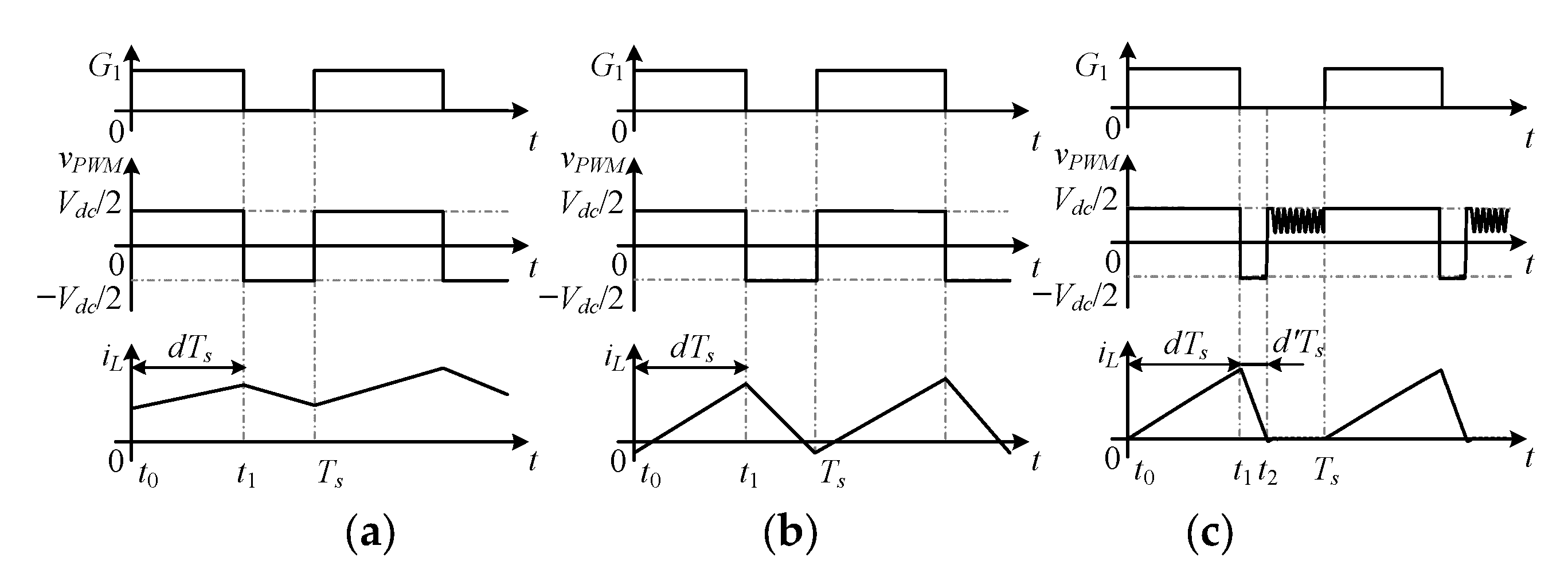
Inverters have been widely used in industrial and residential applications [1,2]. There are three current modes of the filter inductor that can be used for an inverter: continuous conduction mode (CCM), triangular current mode (TCM), and discontinuous conduction mode (DCM). Considering a half-bridge circuit that is shown in Figure 1, the waveforms of the three current modes are shown in Figure 2, where Ts denotes the switching period. The TCM operation can realize the zero-voltage switching (ZVS), which is also called the boundary conduction mode (BCM) [2,3,4], and the DCM operation can realize the zero-current switching (ZCS) [5,6,7,8,9,10].
Both the DCM and TCM are effective ways for reducing the switching loss by soft-switching and lifting the power density using a filter inductor with small inductance [11]. Although the DCM and TCM provide a higher peak inductor current than the CCM [12], their switching losses are acceptable for small-power applications where devices with low turn-off losses can be used [13,14].
The TCM normally operates at a variable switching frequency [3,15,16], and it is realized by controlling the inductor current, i.e., its peak value and the valley value. It can also be regarded as a type of boundary conduction mode (BCM) because its control methods determine the boundary of the inductor current [16].
The main drawback of the TCM is that its switching frequency can vary significantly, which can further lead to excessive turn-off switching losses in power devices, as well as excessive core losses and winding losses of the inductor [1]. Furthermore, the boundary value instead of the average value of the inductor current is required. Therefore, the required frequency of a high-precision accuracy sampling unit is a few times larger than the switching frequency, which leads to high cost. The variable switching frequency makes the closed-loop digital control relatively difficult [17]. In order to solve this problem, some studies have been focused on averaging the switching frequency [1,18]. The TCM with a fixed switching frequency was proposed in [18], but this method can cause larger conduction losses because the RMS value of the inductor current can increase significantly.
In contrast, the DCM can operate at a fixed switching frequency. Moreover, the DCM does not require detecting the inductor current. Therefore, the digital control for the DCM can be realized by using a microprocessor. However, there is still one difficulty: the state average model of the DCM is nonlinear when the capacitor voltage and inductor current are used as state variables. Therefore, no closed-loop control algorithm has been proposed yet.
This paper aims to develop a linear model for the DCM inverter operating at a fixed switching frequency, which is easy and meaningful for performing the closed-loop controls. A linear first-order model named the charge quantity model (CQM), which uses the charge quantities output by the inverter bridge as a control variable, is proposed. In addition, a closed-loop control method named the direct charge control (DCC) method is developed. Finally, the parameter design of the control system is completed. This method can achieve high stability and low distortion of the output voltage. The proportional control can be used for the mentioned control type. Using the proposed control method, the ZCS high-efficiency DCM inverter can operate stably at a fixed switching frequency and achieve accurate sine wave output through digital control. It is also insensitive to device parameter deviation.
The rest of this paper is organized as follows. In Section 2, related works are mentioned and the purposes of the study are stated. In Section 3, a half-bridge inverter with an LC filter for DCM operation is described. The CQM, which is established by using the charge quantities output by the inverter bridge as a control variable, is presented in Section 4, as well as the calculation of the duty cycle. In Section 5, the design procedure of a DCM inverter is introduced. The simulation and experimental results are given in Section 6. Finally, in Section 7, the conclusions are drawn.
2. Overview of Related Work
Nowadays, in the literature, the research on the control of output voltage for the DCM inverter mainly focuses on two problems. One is the optimization of the output voltage waveform distortion around the zero-crossing point of the inductor current. The other is to lower the average switching frequency.
In the inverters designed for CCM, the inductor current still works under DCM around the zero-crossing point of the load current, which causes the serious distortion of output voltage waveform. Research in [19] introduces a judgment and compensation method for DCM in the closed-loop control of the voltage waveform. Reference [10] proposed a power energy modulation (PEM) technique for both DCM and CCM that divided the energy demanded by the load into energy packets and modulated the bridge inverter on the basis of packets of energy for each switching period.
The control methods for the output voltage of DCM inverters are normally realized by using the hysteresis control or the off-time control. However, because the switching frequency is not constant, the extremely high switching frequency may appear and lead to higher switching losses. Reference [11] proposes a variable off-time control method for a single-phase microinverter operating in the DCM to lower the average switching frequency. Furthermore, a fixed off-time control method for single-phase micro-inverter operating in DCM is proposed in [15]. However, the control of output voltage is not discussed.
For the DCM inverter, a closed-loop controller is difficult to design. In [17], a feedforward control was proposed for low-power-grid-tied inverters under DCM, which may increase the switching frequency. In [20], the control of the DCM inverter is based on measuring the boundary of inductor current, and although the inductor current equation is given, it did not provide the digital control method for the output voltage waveform.
In summary, all the above methods cannot guarantee the good waveform of output voltage for the DCM inverter. Even if the switching frequency is fixed, there is still no linear model that has been established. Compared with the existing literature, the charge quantity model is established in this paper, which can solve the problem of the DCM inverter being unable to achieve high-performance closed-loop control due to the absence of a linear model. Furthermore, the closed-loop control method DCC based on CQM was constructed, which is simple to design and achieves a high-quality control effect.
The unique feature of the study in this paper is that a simple first-order linear model is established for the DCM inverter with fixed switching frequency, realizing high-performance closed-loop control.
The purpose of the study in this paper was to achieve a high-performance closed-loop control for DCM inverter. Therefore, a linear first-order mathematical model is firstly proposed, and on the basis of it, the closed-loop control method, named DCC, is constructed. The parameter design of the control system is also completed.
3. DCM Operation Analysis
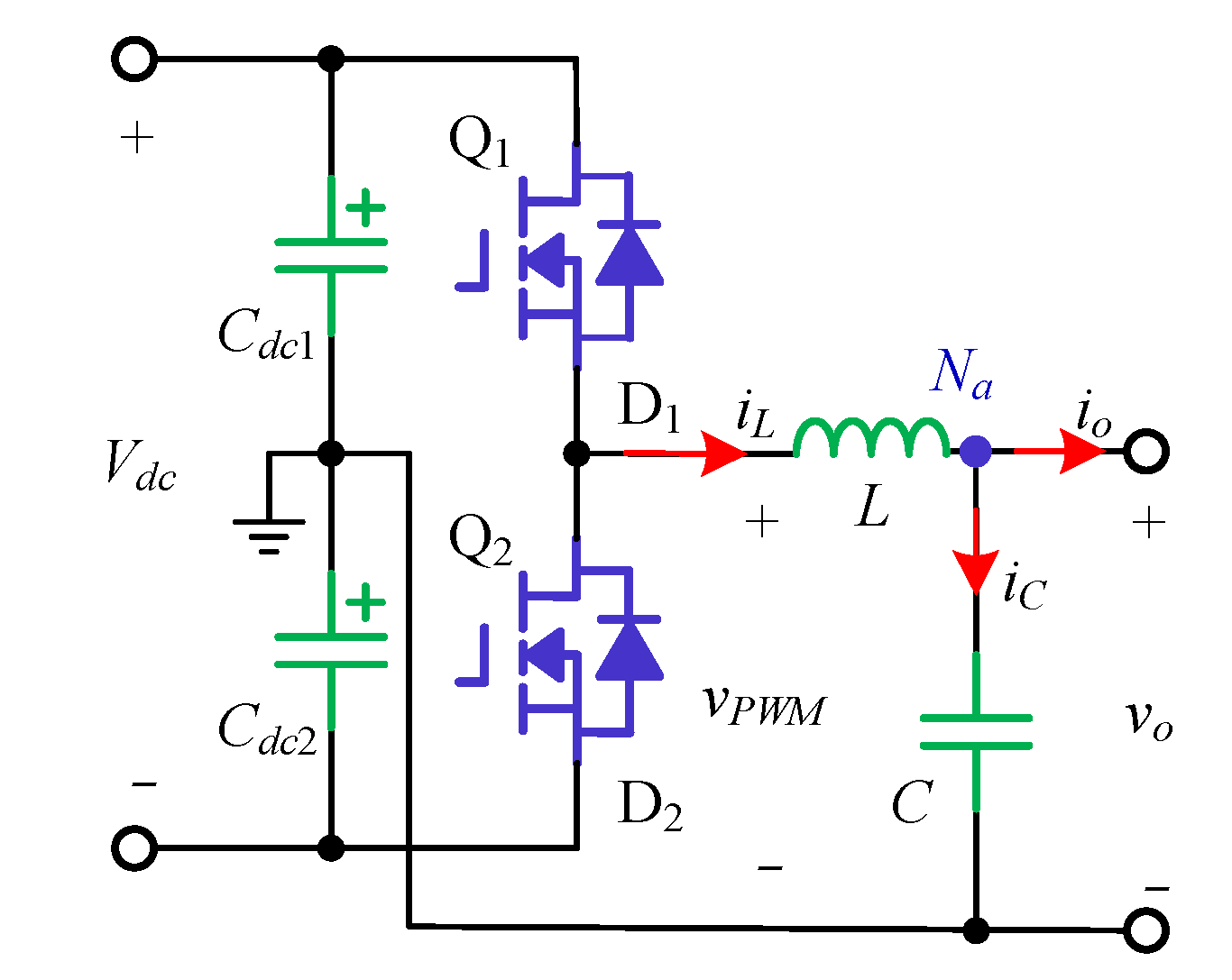
A half-bridge circuit, which is the basic unit of inverters, is shown in Figure 1. It is taken as a research example in this study for analyzing the DCM operation. As shown in Figure 1, the inverter circuit consists of two power devices Q1 and Q2, a filter inductor L, and a filter capacitor C. The DC bus voltage Vdc is separated by two capacitors Cdc1 and Cdc2. The connection point between L and C is denoted as Na.
3.1. DCM
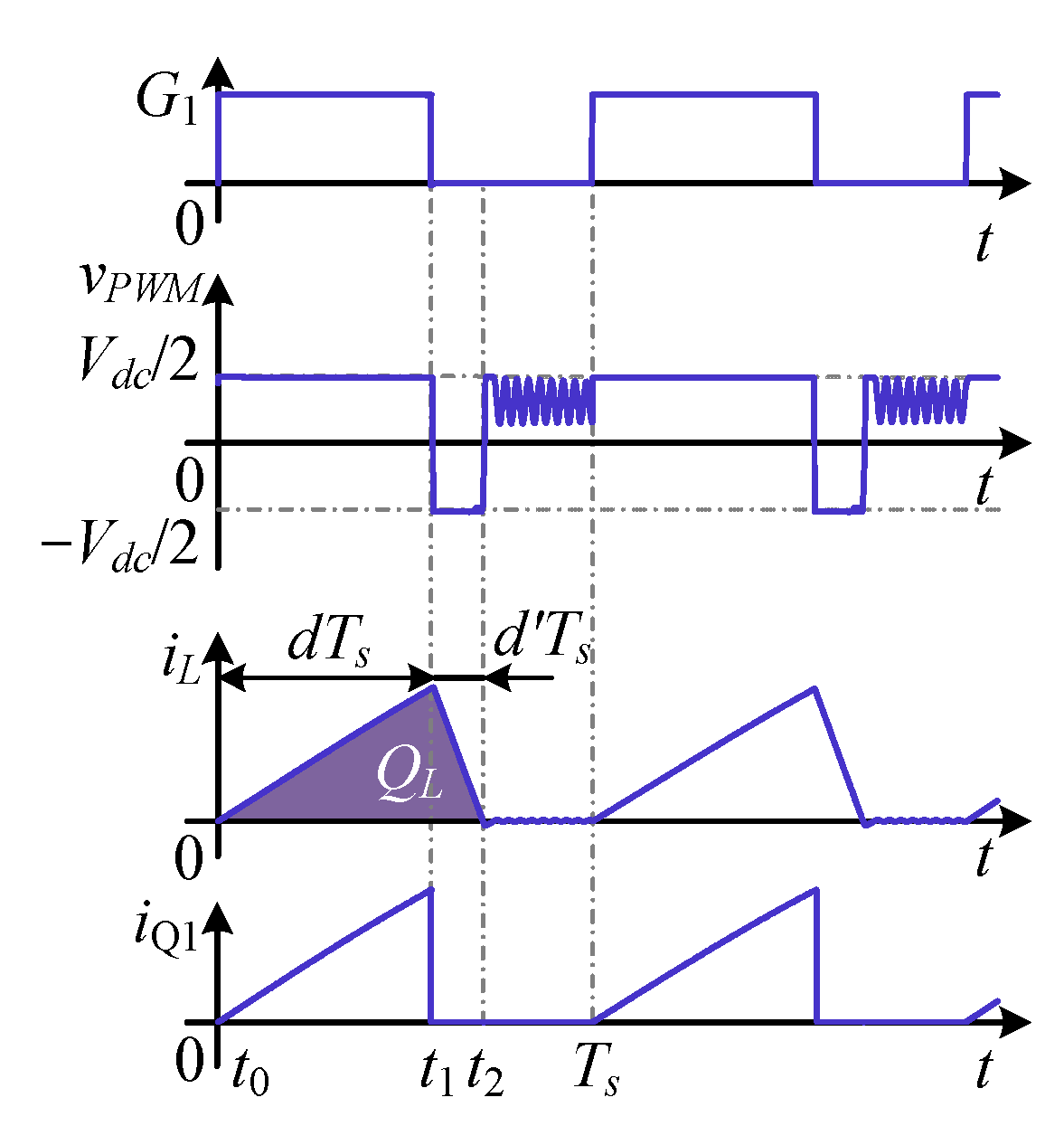
Assume that the inductor current iL and the output inductor voltage vo are positive; then, the steady-state waveforms for one switching cycle are as illustrated in Figure 3. The voltages of Cdc1 and Cdc2 are equal. The switching frequency is high enough, so both vo and Vdc are constant within one switching cycle. The steady-state waveforms for the switching frequency that is much higher than the grid frequency is analyzed in the following.
In one switching cycle, there are three intervals denoted as Intervals I–III.
- Interval I t0~t1: Switch Q1 is turned on at t0; Q1 is ZCS because iL is zero at t0, as shown in Figure 3. In this interval, the DC capacitor Cdc1 charges the filter capacitor C and supports the load current through the inductor L. The inductor voltage is expressed as vL = Vdc/2−vo > 0; thus, iL increases.
- Interval II t1~t2: Switch Q1 is turned off at t1, and the current iL commutates to D2. The inductor voltage is VL = −Vdc/2−vo < 0, and iL decreases to zero at t2.
- Interval III t2~Ts: In this interval, switches Q1 and Q2 keep off. The filter inductor L and the parasitic capacitance of Q1 and Q2 form a resonance circuit, and iL shows a resonant waveform, but its average value is close to zero. The filter inductor L is equivalent to the open circuit, and the load is powered by the filter capacitor C until the next switching cycle starts.
3.2. Circuit Equations
In Intervals I and II, when the inductor current and capacitor voltage are used as state variables, the state equations are given as follows:
In Interval III, when establishing the average model, iL can be considered to be zero, and the state equation in this interval is given by
According to Equations (1) and (2), the linear average state model cannot be derived, which is the reason why the closed-loop controllers for DCM inverter cannot be easily designed.
4. Direct Charge Model and Controller Design
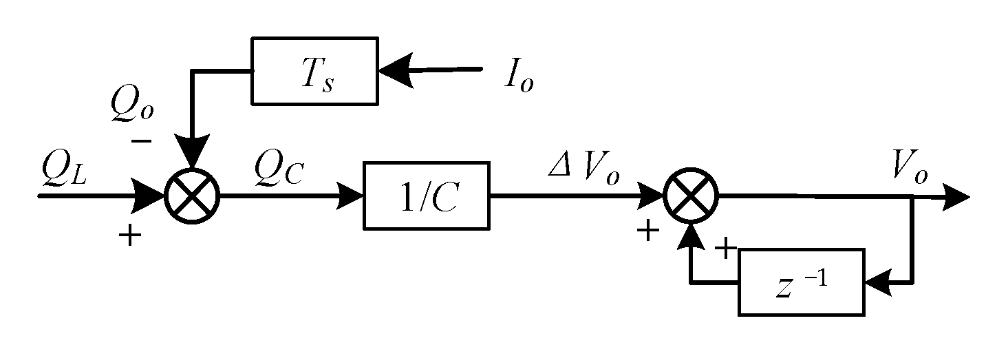
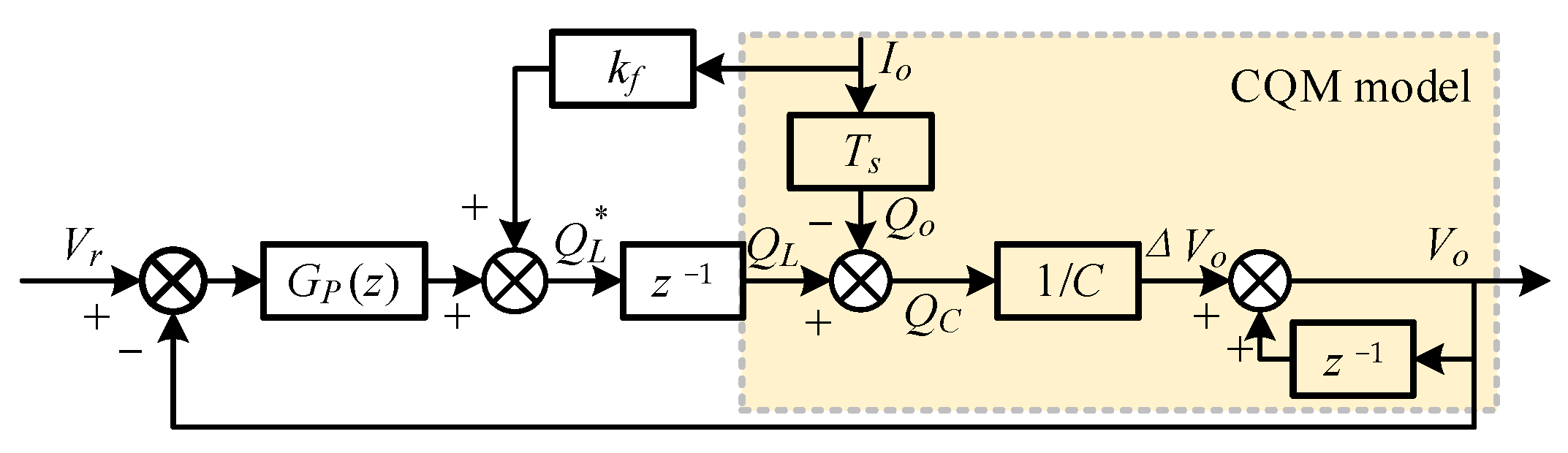
It should be noted that, for node Na, Equation (3) can be applied to the whole switching period, from which the charge equation can be derived as Equation (4). Charges QC and QO flow through the capacitor and load in one switching cycle, respectively. The QL denotes charge output by the inverter bridge, which flow through the inductor. Therefore, the charge quantity QL can be used as a control variable to establish the average model.
4.1. Charge Quantity Model
Equation (4) implies that within a switching period Ts, the amount of charge quantity QL is equal to the sum of the charge quantities QC and QO. Therefore, Equation (4) can be expressed as
Using the Z-transformer, Equation (5) can be expressed as
Equation (6) can be used as a model for the analysis and controller design of a DCM inverter, as shown in Figure 4. It is a linear first-order model, and in this paper, it is called the charge quantity model (CQM). The model uses charge quantity QL as the input control variable and the capacitor voltage Vo as the state and output variables. The load current Io is regarded as a disturbance.
4.2. Duty Cycle Calculation
In practice, the inverter is controlled by the duty cycle d instead of QL. Therefore, the duty cycle calculation is presented in this section.
In Figure 3, the charge quantity QL in one switching period is shown as the shaded area, and it can be realized by the control of duty cycle d. According to the relationship between the inductor voltage and the duty cycle, the inductor current ripple within a switching cycle and the corresponding charge QL can be calculated. The value of QL can be obtained as
In Equation (7), Ton = dTs and Td = d’Ts, as illustrated in Figure 3. Therefore, the inductor current ripple within a switching cycle is given by
From Equation (8), the falling time of the inductor current Td is given by
The inductor current iL decreases to zero before the next switching cycle, and the total duty-ratio dall of the Intervals I and II is calculated as
Therefore, Equation (10) can be rewritten as
On the basis of the required charge quantity QL, the duty cycle d can be determined as Equation (12):
According to Equation (12), when QL is required to output from the bridge, the calculated duty circle d should be applied to switches.
Many factors can affect the realization accuracy of the charge quantity QL, such as the inductance deviation or a DC bus voltage ripple. However, the influence of these disturbances can be suppressed by the closed-loop controller.
4.3. Controller Design
On the basis of the CQM, the closed-loop controllers for the DCM operation can be easily designed. This control method is denoted as the DCC method. The PID controller, PR controller, and voltage and current dual-loop controller can all be used as a controller. Due to the fixed switching frequency, the proposed DCC can be effectively implemented into digital controllers, such as a digital signal processor (DSP). Meanwhile, the proposed DCC does not require high-precision current sampling.
Due to the first-order structure of the CQM model, the simplest controller, which is a proportional controller, can be used. In order to achieve a better response-ability to the step load, the load-current feedforward control is adopted. Considering the one-beat delay, the control method is designed in z domain. The block diagram of the closed-loop control is shown in Figure 5, where the proportional controller is defined by Gp (z) = kp. The one-beat delay caused by the DSP is taken into consideration in the control loop. Although this method cannot be a strong contribution, as shown in [21], it is a good way to check the performance of the mathematic model.
The closed-loop transfer function can be expressed as
where
The characteristic equation of Equation (14) is
Cz + kp − C = 0.
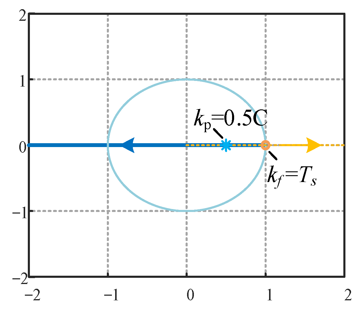
The pole of both Gv(z) and Gi(z) are
Therefore, when kp increases from 0 to +∞, the zp decrease from 1 to −∞, as the blue line given in Figure 6. To ensure the system stable, zp should be inside the unit circle, which means 0 < kp < C.
Considering the transfer function Gi(z), the zero is
z0 is proportional to kf, so it increases as kf increases. Considering the need of achieving the anti-interference ability to the load-current, the amplitude response at the power frequency of the transfer function Gi(z) needs to be close to 0. Therefore, the zero z0 is set to 1 and kf is set as Ts.
Therefore, the parameter of a proportional controller should be 0 < kp < C to ensure the magnitude of pole is |zp| = 1 and kp/C < 1, which means the system is stable.
Furthermore, according to Figure 5, the parameter of load-current feedforward control kf should be similar with Ts to eliminate the influence of the load current as much as possible.
5. LC Filter Design
In order to ensure that the inverter can work under the DCM for all switching periods, it is necessary to choose the LC filter parameters and switching frequency properly. Therefore, this section provides a design reference for DCM inverters.
The basic parameters of the inverter design include the DC voltage Vdc, the RMS value of the output AC voltage Vorms, the rated power PN, the peak value of inductor current IL, and the switching frequency fs. Furthermore, on the basis of the proposed model, the maximum value of dall = d + d’, which is denoted as Dmax, was set as a design parameter. First of all, the inverter working in the DCM operation mode must satisfy the following condition d + d’ ≤ 1. Considering the step load and other disturbances, Dmax should be smaller than one, and it was set to 0.95 in this paper.
According to Equation (10), the maximum of QL is limited by the available duty cycle, which can be defined as QLlim:
A well-designed inductance should make sure that the output charge ability QLlim is greater than the charge spends on the load in any switching period. In the case of full-resistive load, QLlim reaches its minimum at the peak value of the AC output voltage vo. At the same time, the charge spent on load also reaches its maximum. Therefore, the value of the inductance L is designed to the charge transfer capability at the peak value of the AC output voltage under the rated power of the resistive load, as shown in Equation (18).
Thus, the limitation of inductance L is expressed as
The high frequency components of the inductor current iL flow through the filter capacitor C and cause high-frequency ripple in the output voltage. The value of the filter capacitor should be designed as Equation (20) to effectively reduce the ripple of the output voltage ΔVpp.
where ILpeak denotes the peak value of the inductor current.
In DCM, the inductance of the filter inductor can be greatly reduced. However, due to the large ripple of the inductor current, it is necessary to increase the capacitance of the filter capacitor to absorb the harmonic current of the switching frequency. However, this will not significantly increase the volume of the capacitor. On the other hand, because the direct charge control method has a good control effect, it can effectively reduce the low harmonic of the output voltage. Therefore, the proposed method will not cause significant harmonic impact on the close equipment.
6. Simulation and Experimental Results
The simulation results verified the results given in Section 5. The simulation and experimental parameters are given in Table 1.
6.1. Simulation Results
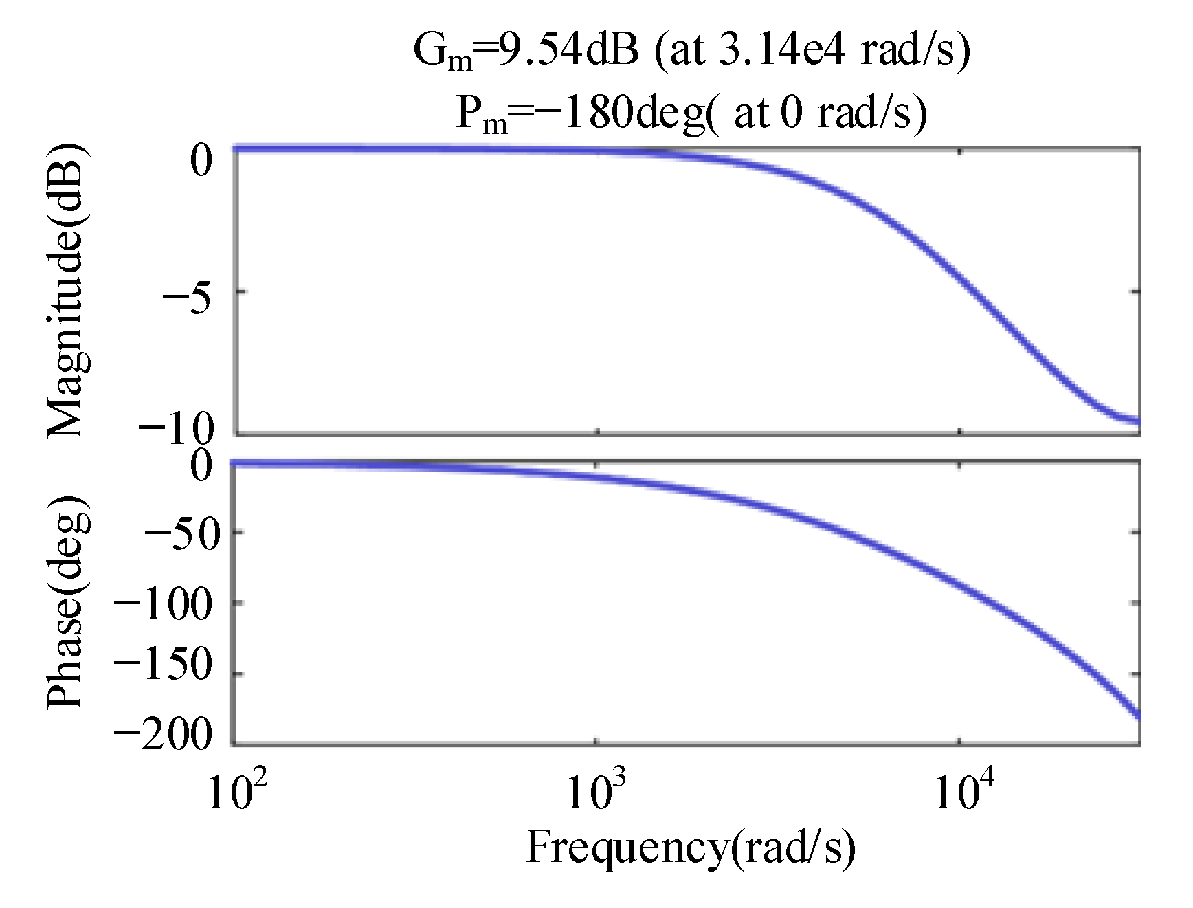
According to Equation (14), the controller parameter was set as kp = 0.5C, and kf = Ts was adopted to suppress the load current disturbance effectively.
The bode diagram can be given as Figure 7 and shows that the system is stable.
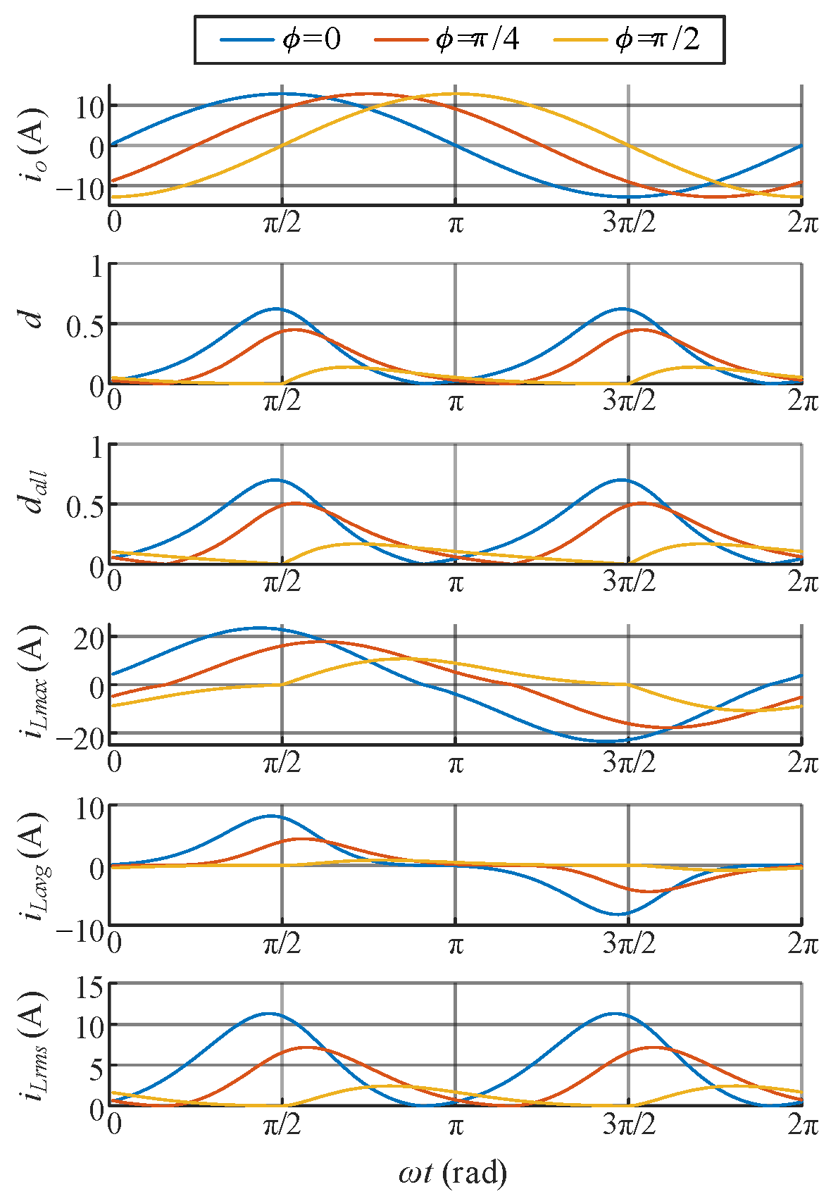
The output current io, the duty cycle d, the total duty cycle dall, the current stress ΔiL, the average value of inductor current iLavg, and the RMS value of the inductor current iLrms for a different power factor angle ϕ of the load are presented in Figure 8. As shown in Figure 8, when the power factor angle was ϕ = 0, both the duty cycle and the inductor current were the largest. Therefore, if the designed inverter can work well under the resistance load, it can also work well under other conditions.
6.2. Experimental Results
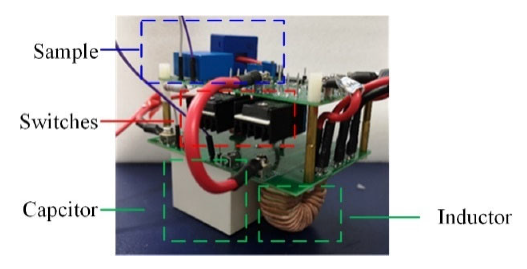
The proposed CQM and DCC methods were verified by the experiment using a 1 kW prototype, as shown in Figure 9. The experimental parameters are shown in Table 1. The Si MOSFETs were used as switching devices to take advantage of low turn-off losses and low conduction losses. The controller used in the prototype was based on a DSP TMS320F28335.
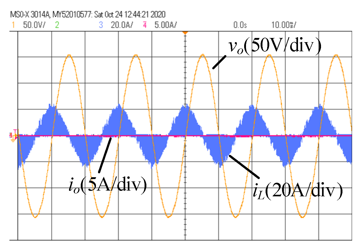
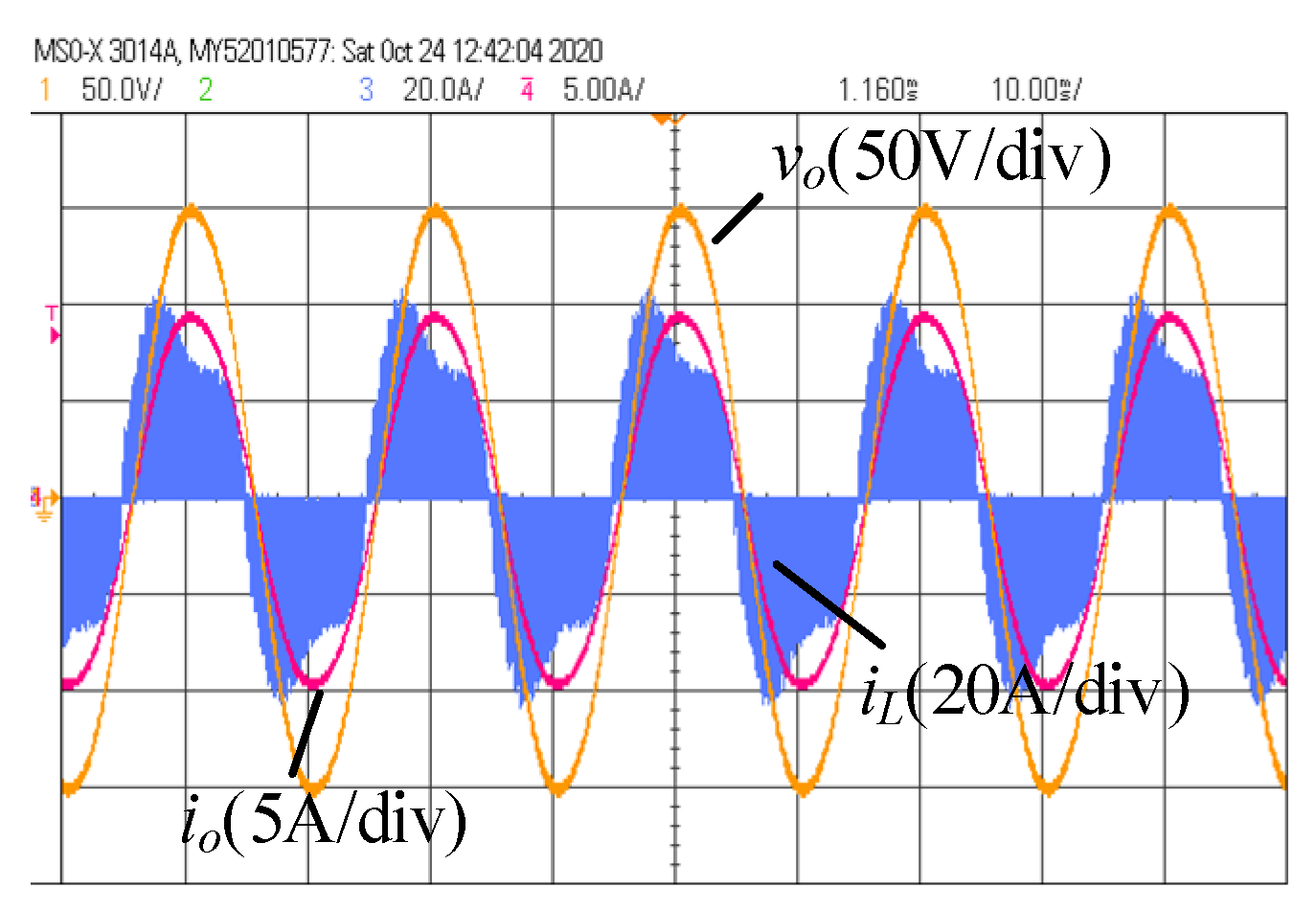
The waveforms of the inverter with no-load and under a resistive load are shown in Figure 10 and Figure 11, respectively, where it can be seen that the system could stably output the sine wave, and its THD was 2.77% at Po = 1 kW.
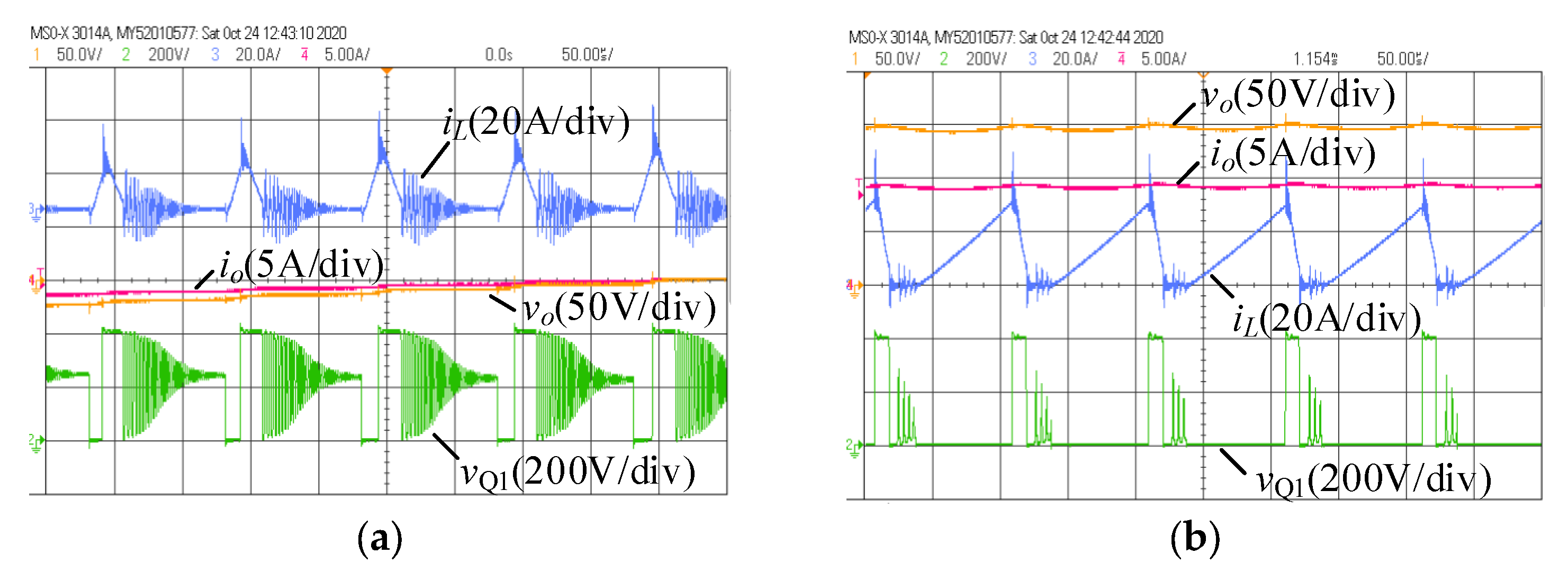
The zoomed-in waveforms of Figure 11 at different output voltage values, including vo = 0 and 150 V, are illustrated in Figure 12. The drain-source voltage of active switch VQ1 and inductor current iL for DCM operation is illustrated in Figure 12, where the output voltage vo and output current io are also given as a reference. As shown in Figure 12, the active switch was always under ZCS turn-on. What is more, the oscillating waveforms on iL and VQ1 were due to the resonance caused by the inductor and the parasitic capacitance of the switching devices in the corresponding interval in which both switches were turned off.
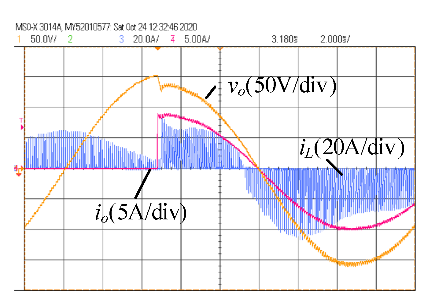
As shown in Figure 13, when the step load was applied, the voltage sag was 25.5 V, and the corresponding drop time was 0.4 ms, which was about four switching periods. In Figure 13, it can be seen that the proposed DCC method had good dynamic performance while using the proportional feedback controller plus the proportional load current feedforward controller. It should be noted that PID control, PR control, and other control methods can also be easily adopted in the proposed method if higher performance is required, but due to the limitation on the paper length, this is not discussed in this paper. Furthermore, although the inductor current maximum value of the inverter under no load and under the resistive load were similar, the duty cycles were different, as given in Equation (12). Under very small QL and d, the conduction losses in the no-load situation were much smaller than those in the full-load situation.
The losses of the inverter consists of inductor loss and switching device loss. For the soft-switching turn-on being realized by operating in DCM, the switching device losses include the turn-off losses and the conduction losses. The losses can be calculated by
where RL is the total equivalent resistance of inductor, d denotes the duty ratio of the current passing through a power device, Ron represents on-state equivalent resistance of MOSFET, VD represents on-state voltage drop of the body diode at zero current, RD represents its on-state equivalent resistance, and koff1–koff3 are the corresponding coefficient of turn-off losses. According to the datasheet, the parameters using for losses calculation are listed in Table 2.
Taking the positive half period as an example, the current goes through MOSFET when Q1 is turned on, and goes through the body diode of Q2 when Q1 is turned off and current is still not zero.
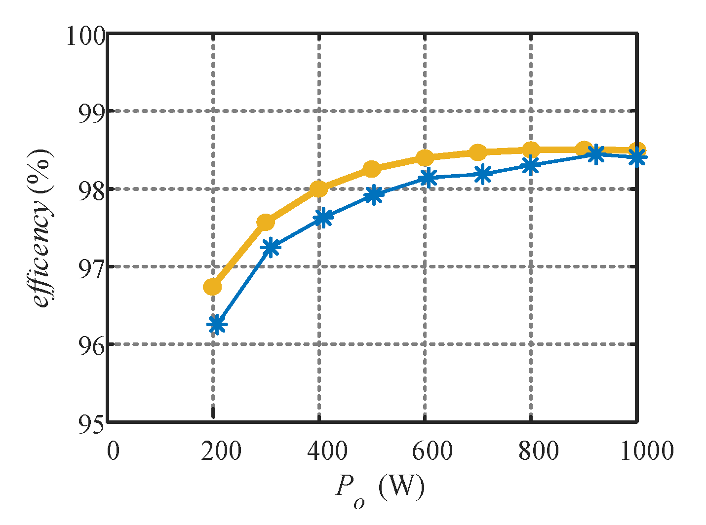
The efficiency of the experimental prototype, including the DC capacitors, half-bridge leg, and LC filter, was tested by the power analyzer. The comparison of the theoretical efficiency curve and experimental efficiency curve is given in Figure 14, where it can be seen that the peak efficiency of measured efficiency was above 98%. What is more, the efficiency curve obtained by the theoretical calculation was similar to the experimental efficiency curve and slightly higher than the experimental efficiency measured by the experiment. The error was mainly caused by the inconsistency between the operating temperature and parasitic parameters of the switch tube under the experimental conditions and the test conditions set in the data sheet.
In particular, the DCC could achieve high efficiency at a low load. The efficiency of the inverter can be further improved by optimization of the inductor design.
7. Conclusions
This paper proposes a CQM model for the inverter under the DCM operation. The proposed model uses the charge quantity output by the inverter bridge as a control variable to realize a linear model that has a simple first-order structure. This model is convenient for the simple realization of digital closed-loop control in a DCM inverter with a fixed switching frequency. The combination of the proportional controller and load current feedforward controller can provide good performances regarding the dynamic response and steady-state sine wave output.
Since the fixed frequency control is realized, the control system can be easily designed. Benefiting from the closed-loop control, the proposed DCM inverter is immune to the change in hardware parameters and does not require high-precision current sampling. The DCC can achieve high efficiency at a low load.
The key points of this paper’s contribution are summarized as follows:
- This paper proposed a mathematical model based on charge quantity. The model has a simple first-order linear structure and it is easy to design the closed-loop control.
- On the basis of the charge quantity model, a direct charge control method was proposed, and the performance was verified by the experiments using a 1 kW prototype, and a high-quality output voltage waveform with a peak efficiency of above 98% was achieved.
The proposed control method for the DCM provides a good solution for low AC power supply applications.
Author Contributions
Conceptualization, Y.Z. and Q.G.; methodology, Q.G.; software, Q.G.; validation, Q.G.; formal analysis, Y.Z. and Q.G. investigation, Q.G.; resources, Y.Z.; data curation, Q.G.; writing—original draft preparation, Q.G.; writing—review and editing, Y.Z.; visualization, Q.G.; supervision, Y.Z.; project administration, Y.Z. and Q.G.; funding acquisition, Q.G. All authors have read and agreed to the published version of the manuscript.
Funding
This research presented in this work was supported by the National Natural Science Foundation of China under grant no. 51907071.
Institutional Review Board Statement
Not applicable.
Informed Consent Statement
Not applicable.
Data Availability Statement
Not applicable.
Conflicts of Interest
The authors declare no conflict of interest.
References
- Liu, T.; Chen, C.; Xu, K.; Zhang, Y.; Kang, Y. GaN-Based MHz Single Phase Inverter with a Hybrid TCM Control Method for High Efficiency and High-Power Density. IEEE Trans. Power Electron. 2021, 36, 6797–6813. [Google Scholar] [CrossRef]
- Cimendağ, A.; Duman, T.; Yılmaz, M. 250W GaN Hybrid BCM Micro-Inverter Design for Avionic Applications. In Proceedings of the 2022 IEEE Applied Power Electronics Conference and Exposition (APEC), Houston, TX, USA, 20–24 March 2022; pp. 838–842. [Google Scholar]
- Marxgut, C.; Biela, J.; Kolar, J.W. Interleaved Triangular Current Mode (TCM) Resonant Transition, Single Phase PFC Rectifier with High Efficiency and High Power Density. In Proceedings of the The 2010 International Power Electronics Conference—ECCE ASIA, Sapporo, Japan, 21–24 June 2010; pp. 1725–1732. [Google Scholar]
- Allemann, S.; Biela, J.; Held, M. Reliability Comparison of a Dual Boost and a Triangular Current Mode Resonant-Transition PFC Converter Topology. In Proceedings of the 2012 7th International Conference on Integrated Power Electronics Systems (CIPS), Nuremberg, Germany, 6–8 March 2012; pp. 1–5. [Google Scholar]
- Dalapati, S.; Chakraborty, C. A Direct PWM Technique for a Single-Phase Full-Bridge Inverter through Controlled Capacitor Charging. IEEE Trans. Ind. Electron. 2008, 55, 2912–2922. [Google Scholar] [CrossRef]
- Chakraborty, C.; Dalapati, S.; Bhattacharya, S. Performance Evaluation of Controlled-Capacitor-Charging-Type Inverters. IEEE Trans. Ind. Electron. 2009, 56, 12–19. [Google Scholar] [CrossRef]
- Chakraborty, C.; Dalapati, S.; Bhattacharya, S. Variable Frequency Variable Duty Cycle Operation of the Controlled Capacitor Charging (CCC) Type Inverter. In Proceedings of the 31st Annual Conference of IEEE Industrial Electronics Society, IECON 2005, Raleigh, NC, USA, 6–10 November 2005; pp. 598–603. [Google Scholar]
- Dalapati, S.; Chakraborty, C.; Bhattacharya, S. Single Phase, Full Bridge, Controlled Capacitor Charging (CCC) Type Inverter. In Proceedings of the 2006 IEEE International Conference on Industrial Technology, Mumbai, India, 15–17 December 2006; pp. 265–270. [Google Scholar]
- Vijayakumar, K.; Rajan, S.E. Performance Evaluation of Inverter Topology Employing Controlled-Capacitor-Charging Technique. In Proceedings of the 2011 International Conference on Emerging Trends in Electrical and Computer Technology, Nagercoil, India, 23–24 March 2011; pp. 398–406. [Google Scholar]
- Xu, S.; Cao, B.; Chang, L.; Shao, R. Pulse Energy Modulation for a Single-Phase Bridge Inverter with Active Power Decoupling Capability. IEEE J. Emerg. Sel. Top. Power Electron. 2021, 9, 2014–2026. [Google Scholar] [CrossRef]
- Zhang, Z.; Zhang, J.; Shao, S. A Variable Off-Time Control Method for a Single-Phase DCM Microinverter. IEEE Trans. Power Electron. 2018, 33, 7229–7239. [Google Scholar] [CrossRef]
- Prasad, B.S.; Jain, S.; Agarwal, V. Universal Single-Stage Grid-Connected Inverter. IEEE Trans. Energy Convers. 2008, 23, 128–137. [Google Scholar] [CrossRef]
- Appel, T.; Fuhrmann, J.; Eckel, H. Design of Inductive Components for Triangular Current Mode (TCM) Inverters up to 500 KW. In Proceedings of the PCIM Europe 2017, International Exhibition and Conference for Power Electronics, Intelligent Motion, Renewable Energy and Energy Management, Nuremberg, Germany, 16–18 May 2017; pp. 1–7. [Google Scholar]
- Erickson, R.W.; Rogers, A.P. A Microinverter for Building-Integrated Photovoltaics. In Proceedings of the 2009 Twenty-Fourth Annual IEEE Applied Power Electronics Conference and Exposition, Washington, DC, USA, 15–19 February 2009; pp. 911–917. [Google Scholar]
- Zhang, Z.; Zhang, J.; Shao, S.; Wu, X.; Sheng, K. A Novel Fixed Off-Time Control Method for Single-Phase Micro-Inverter without Sensing Inductor Current. In Proceedings of the 2017 IEEE 3rd International Future Energy Electronics Conference and ECCE Asia (IFEEC 2017—ECCE Asia), Kaohsiung, Taiwan, 3–7 June 2017; pp. 1886–1891. [Google Scholar]
- Wang, J.; Zhang, D.; Liu, J.; Lv, Z.; Li, Y. Digital ZVS BCM Current Controlled Single-Phase Full-Bridge Inverter Using DSP TMS320F28035. In Proceedings of the 2017 IEEE 3rd International Future Energy Electronics Conference and ECCE Asia (IFEEC 2017—ECCE Asia), Kaohsiung, Taiwan, 3–7 June 2017; pp. 857–860. [Google Scholar]
- Zhang, J.; Isobe, T.; Tadano, H. Model-Based Control for Grid-Tied Inverters Operated in Discontinuous Current Mode with Low Harmonic Current Distortion. IEEE Trans. Power Electron. 2020, 35, 11167–11180. [Google Scholar] [CrossRef]
- Rothmund, D.; Bortis, D.; Huber, J.; Biadene, D.; Kolar, J.W. 10kV SiC-Based Bidirectional Soft-Switching Single-Phase AC/DC Converter Concept for Medium-Voltage Solid-State Transformers. In Proceedings of the 2017 IEEE 8th International Symposium on Power Electronics for Distributed Generation Systems (PEDG), Florianopolis, Brazil, 17–20 April 2017; pp. 1–8. [Google Scholar]
- Xu, S.; Cao, B.; Chang, L.; Zhou, J. Hybrid Modulation and Power Decoupling Control on Single-Phase Bridge Inverter with Buck-Boost Converter. IEEE J. Emerg. Sel. Top. Power Electron. 2021, 9, 5851–5864. [Google Scholar] [CrossRef]
- Isobe, T.; Kato, K.; Kojima, N.; Shimada, R. Soft-Switching Single-Phase Grid-Connecting Converter Using DCM Operation and a Turn-Off Snubber Capacitor. IEEE Trans. Power Electron. 2014, 29, 2922–2930. [Google Scholar] [CrossRef]
- Uesugi, S.; Mannen, T.; Isobe, T. Feed-Forward Current Control for Filter Size Reduction in a Sinusoidal Voltage Output Inverter for IPMSM Drive. In Proceedings of the 2020 23rd International Conference on Electrical Machines and Systems (ICEMS), Hamamatsu, Japan, 24–27 November 2020; pp. 662–667. [Google Scholar]
Figure 1.
The circuit of a single-phase half-bridge inverter.

Figure 2.
Schematic diagram of different current modes: (a) CCM, (b) TCM, (c) DCM.

Figure 3.
The DCM operation waveforms of the inverter.

Figure 4.
The CQM block diagram of a DCM inverter.

Figure 5.
The DCC control diagram of a DCM inverter.

Figure 6.
Zero-pole plot of transfer function.

Figure 7.
The bode diagram of the control system (kp = 4 × 10⁻⁵ and C = 80 µF).

Figure 8.
The calculation results at fs = 10 kHz, L = 120 μH, and C = 80 µF.

Figure 9.
The image of the DCM inverter prototype.

Figure 10.
The voltage and current waveforms of the DCM inverter at Po = 0. Time: 10 ms/div.

Figure 11.
The voltage and current waveforms of the DCM inverter at Po = 1 kW. Time: 10 ms/div.

Figure 12.
Waveforms of the active switch drain-source voltage and inductor current for the DCM operation at 1 kW: (a) vo = 0, (b) vo =150 V (time: 50 μs/div).
Figure 12.
Waveforms of the active switch drain-source voltage and inductor current for the DCM operation at 1 kW: (a) vo = 0, (b) vo =150 V (time: 50 μs/div).

Figure 13.
Dynamic response of the inverter to the step-change in the output power from 0 to 1 kW. Time: 2 ms/div.
Figure 13.
Dynamic response of the inverter to the step-change in the output power from 0 to 1 kW. Time: 2 ms/div.

Figure 14.
Efficiency curve of the closed-loop control DCM inverter.


Table 1.
Simulation and experimental parameters.
| Input voltage | 400 Vdc | Output voltage | 110 Vrms |
| Switching frequency | 10 kHz | Output power | 1 kW |
| Dmax | 0.95 | ||
| ILpeak | 30 A | ΔVpp | 10 V |
| Lmax | 126.04 μH | Cmin | 75 μF |
| Filter inductor L | 120 μH | Filter capacitor C | 80 μF |
| kp | 4 × 10⁻⁵ | kf | 1 × 10⁻⁴ |
| Switch | IPW65R048CFDA (650 V/40 A) | ||
Table 2.
Parameters used for loss calculation.
| RL (W) | 0.15 | Vswi(V) | 400 |
| Rdson (W) | 0.043 | koff1 | 1.03 × 10⁻⁷ |
| VD (V) | 0.28 | koff2 | 1.01 × 10⁻⁵ |
| RD (W) | 0.005 | koff3 | 2.53 × 10⁻⁶ |
Publisher’s Note: MDPI stays neutral with regard to jurisdictional claims in published maps and institutional affiliations. |
© 2022 by the authors. Licensee MDPI, Basel, Switzerland. This article is an open access article distributed under the terms and conditions of the Creative Commons Attribution (CC BY) license (https://creativecommons.org/licenses/by/4.0/).
Share and Cite
MDPI and ACS Style
Guan, Q.; Zhang, Y. Direct Charge Control Method for Inverters in Discontinuous Conduction Mode. Energies 2022, 15, 6608. https://0-doi-org.brum.beds.ac.uk/10.3390/en15186608
AMA Style
Guan Q, Zhang Y. Direct Charge Control Method for Inverters in Discontinuous Conduction Mode. Energies. 2022; 15(18):6608. https://0-doi-org.brum.beds.ac.uk/10.3390/en15186608
Chicago/Turabian StyleGuan, Qingxin, and Yu Zhang. 2022. "Direct Charge Control Method for Inverters in Discontinuous Conduction Mode" Energies 15, no. 18: 6608. https://0-doi-org.brum.beds.ac.uk/10.3390/en15186608
Note that from the first issue of 2016, this journal uses article numbers instead of page numbers. See further details here.