
Analysis and Modeling of a Single-Power-Source T-Type 7-Level Single-Phase DC-AC Inverter with Voltage Gain of 3


1
Department of Electrical Engineering, Feng Chia University, No. 100, Wenhwa Road, Seatwen, Taichung 40724, Taiwan
2
Department of Electrical Engineering, National Taipei University of Technology, 1, Sec. 3, Zhongxiao E. Road, Taipei 10608, Taiwan
3
Delta Electronics (Taiwan), No. 16, Dongyuan Road, Zhongli Dist., Taoyuan City 32063, Taiwan
*
Author to whom correspondence should be addressed.
Energies 2022, 15(21), 7894; https://0-doi-org.brum.beds.ac.uk/10.3390/en15217894
Submission received: 13 September 2022
/
Revised: 11 October 2022
/
Accepted: 14 October 2022
/
Published: 24 October 2022
(This article belongs to the Special Issue Multilevel Converter Topology, Design, and Applications)
Abstract
:This paper proposes a novel T-type 7-level single-phase DC-AC inverter having a single input power source, self-balancing, and voltage gain of 3 along with low total harmonic distortion (THD). Since the structure of the proposed 7-level DC-AC inverter is symmetrical, the interchangeability of mass production can be easily achieved. In addition, because only one switch works for all time, the switch has quite low switching loss and voltage stress as well as the control being very easy. Furthermore, not only the proposed 7-level DC-AC inverter is analyzed in detail by the operating principle, but also the mathematical model for the adopted level-shift sinusoidal pulse width modulation (LS-SPWM) for this multilevel DC-AC inverter is successfully developed by using the well-known state averaging technique widely employed in the DC-DC converter. As a result, the required proportional-integral (PI) controller, used in the closed loop, can be designed systematically and easily. Eventually, the feasibility and effectiveness of the proposed inverter are verified by simulated and experimental results.
1. Introduction
1.1. Motivations
Multilevel DC-AC inverters (MLIs) are a popular solution for AC power sources, including renewable energy conversion such as wind energy [1,2], automotive [3,4,5,6], and photovoltaic application [3,7,8]. Compared to two-level voltage source inverters, MLIs have the advantages of low voltage stress, high efficiency, low common-mode voltage, as well as providing high quality output waveforms and improving the total harmonic distortion (THD) [9].
The basic operating principle of the multilevel DC-AC inverter is to utilize the switch path to render the output voltage stratified, and to upgrade the number of filters or levels to cause the output voltage to be sinusoidal-like. As the output voltage of an MLI is hierarchical, the voltage stress across the switch can be clamped. As a result, the high-voltage AC output can be realized by low-voltage components.
MLIs can be used in high power or low power. Generally, high power converters have the advantage that all semiconductors are rated to the same voltage, despite the ratio of output levels over the number of power semiconductors being relatively low compared to low power converters. Low power multilevel inverters are also a wide research field in which a large number of output voltage levels can be achieved by sacrificing the voltage rating of semiconductors. For switching topologies, on the other hand, MLIs can be divided into two major categories, containing step switching multilevel and pulse-width-modulated (PWM) switching multilevel.
The step switching multilevel DC-AC inverter employs DC power source, semiconductor elements and capacitors to synthesize the AC output voltage [10,11,12]. Although this inverter greatly reduces the number of switching cycles over one AC cycle, the DC-AC conversion current path is increased by too many semiconductor elements, thereby increasing turn-on loss. Furthermore, since multilevel DC-AC inverters operate at low frequencies, the switched capacitors require a large capacity to provide step voltages. In addition, the load dynamic response of such an inverter is rather slow.
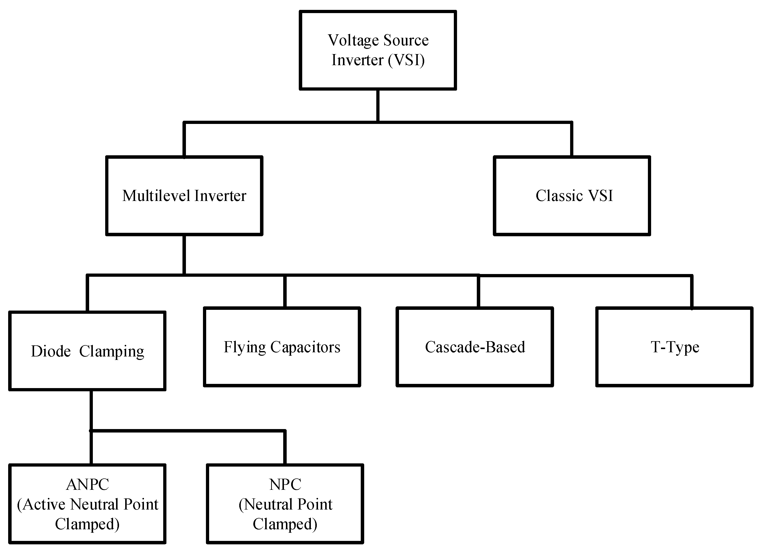
Voltage source multilevel PWM switching DC-AC inverters can be mainly classified into four types, containing flying capacitor type, cascade type, diode clamp type, and T-Type. The diode clamp type can be furthermore classified into two types: one is neutral point clamped (NPC), the other is active neutral point clamped (ANPC). In general, the voltage-type multilevel DC-AC inverters can be classified by Figure 1.
The flying-capacitor-based multilevel DC-AC inverter is designed to achieve the AC output voltage clamped by interconnecting multiple capacitors [13,14]. However, a large number of capacitors and complicated control strategies for capacitor voltage balancing are required to obtain a stratified output voltage.
The cascade-based multilevel DC-AC inverter is the only type having a modular design concept and adopts the fewest components among the three types [15,16]. However, the need for multiple independent power supplies to synthesize the required levels of the AC output voltage limits its applications.
The diode-clamp-based multilevel DC-AC inverter employs a diode and a switch to generate the potential of the neutral point for the output voltage, and a PWM (Pulse Width Modulation) method to create the appropriate gate signal to turn on the switch. This results in lower harmonic components compared to the traditional 2-level DC-AC inverter [17,18,19]. However, the diode clamp circuit has the problem of not achieving self-balancing at high levels [19].
The conventional T-type active clamp DC-AC inverter uses fewer components than the flying capacitor and the diode clamped DC-AC converters, and the voltage stress on the switch is lower than the input voltage. In addition, complex control signals are not required to balance the capacitor voltage. However, this structure requires two capacitors to build up the neutral point voltage and a bidirectional switch to connect the neutral point to the load, leading to only a 3-level step-down output voltage.
1.2. State of the Related Works
There are many other existing papers presented for the T-type single-phase MLIs [20,21,22,23,24,25] with a different number of levels, voltage gain and circuit structure considered. Those characteristics are summarized in Table 1. In study [20], two structures are presented by combining a T-type active clamp DC-AC inverter with multiple DC power sources. The first structure uses three DC voltage sources and ten switches to achieve a 15-level AC output with a voltage gain of 1, while the second structure uses four DC power sources and twelve switches to achieve a 25-level AC output with a voltage gain of 1. In studies [21,22,23], two T-type active clamp DC-AC inverters are used to form the circuit structure. In study [21], the input capacitance of the second T-type active clamp DC-AC inverter is changed to the power source voltage, and a 7-level step-up T-type DC-AC inverter having a voltage gain of 1.5 is implemented with ten switches and four capacitors. In study [22], only one capacitor is employed to boost the voltage, an inductor is utilized at the front end of the capacitor to form a buck-boost converter, and a duty cycle of 0.5 is adopted to convert the voltage on the capacitor to the power source voltage to achieve a 5-level AC output with a voltage gain of 2. The circuit structure shown in [23] takes four power inputs cross-connected to obtain two T-type actively clamped DC-AC inverters to achieve a 9-level AC output with a voltage gain of 1. However, compared with studies [21,22], the input power source is increased from a single power source to four power sources, but the 7- and 5-level DC-AC inverters in [21,22], respectively, are upgraded to the 9-level ones. In studies [24,25], 7-level DC-AC inverters are presented, formed by combining the T-type active clamp DC-AC inverter with the H-bridge. In study [24], eight switches and one floating capacitor are used to form a 7-level DC-AC inverter possessing a voltage gain of 0.75, and the space vector modulation is used to maintain the floating capacitor across the H-bridge at half of the DC input voltage. Compared with study [18], the literature [19] adds two switches to achieve a 7-level AC output with a voltage gain of 1.5.
On the other hand, in order to control the power converter, modeling is very important, although there are, of course, numerous variations in analysis and measure from a theoretical and implement point of view, respectively [26]. There are many methods which were proposed for modeling the DC-DC converter, for example, the well-known state-space averaging method. However, very few examples of modeling the multilevel DC-AC inverter can be found in the literature.
1.3. Contributions
Contributions of this paper are as follows: (1) A novel T-type 7-level single-phase DC-AC inverter with a single input power source, self-balancing, voltage gain of 3 and low total THD is proposed, which is different from [27] based on class-D. (2) The mathematical model of the DC-AC inverter is successfully developed by using the well-known state-space averaging method widely used in the DC-DC converter. (3) A 300 W prototype circuit is simulated to demonstrate the feasibility of the proposed circuit, and one-comparator voltage control [28], accordingly to the field programmable gate array (FPGA), which is utilized to verify the effectiveness of the proposed circuit. The proposed T-type 7-level DC-AC inverter not only has a rather fast load transient response due to the well-designed feedback controller, but also has the efficiency up to 97.42% and the THD down to 2.01%.
The contents of the paper may be outlined as follows. Section 2 illustrates the proposed MLI, including circuit description, switching patterns, and operating principle. Power component design is given in Section 3. Modeling and controller design is introduced for the level-shift sinusoidal pulse width modulation (LS-SPWM) in Section 4. Simulated and experimental results, along with discussions, are shown in Section 5. Finally, some conclusions are made in the last section.
2. Proposed Inverter
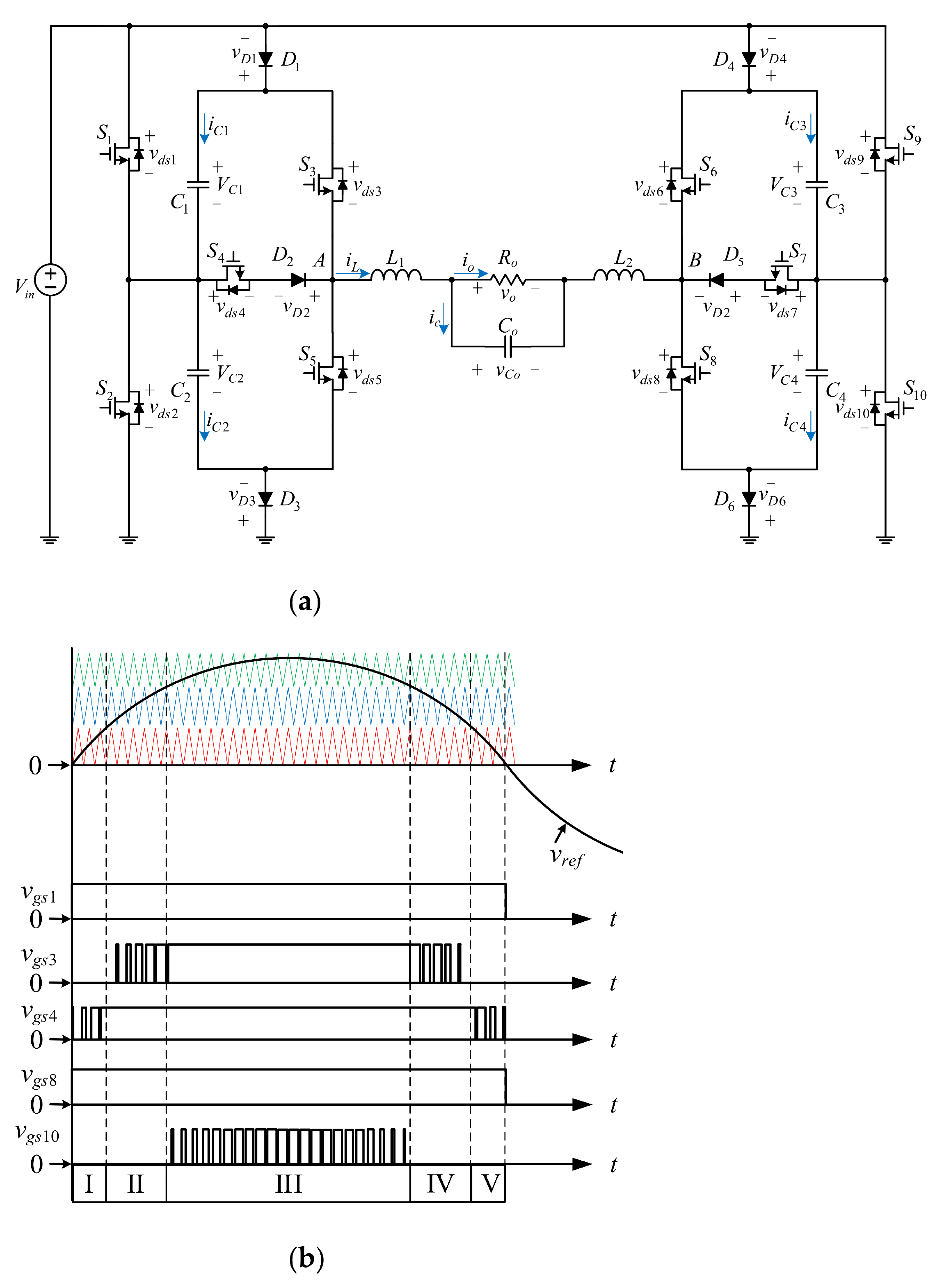
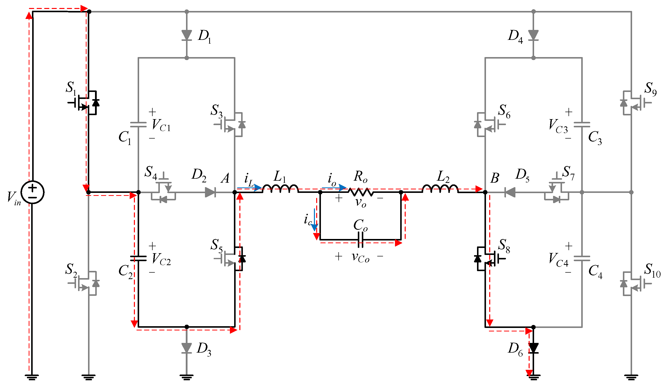
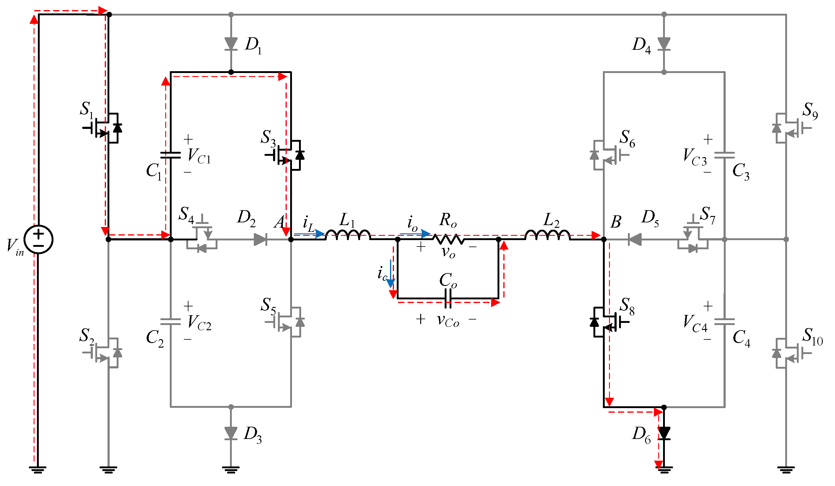
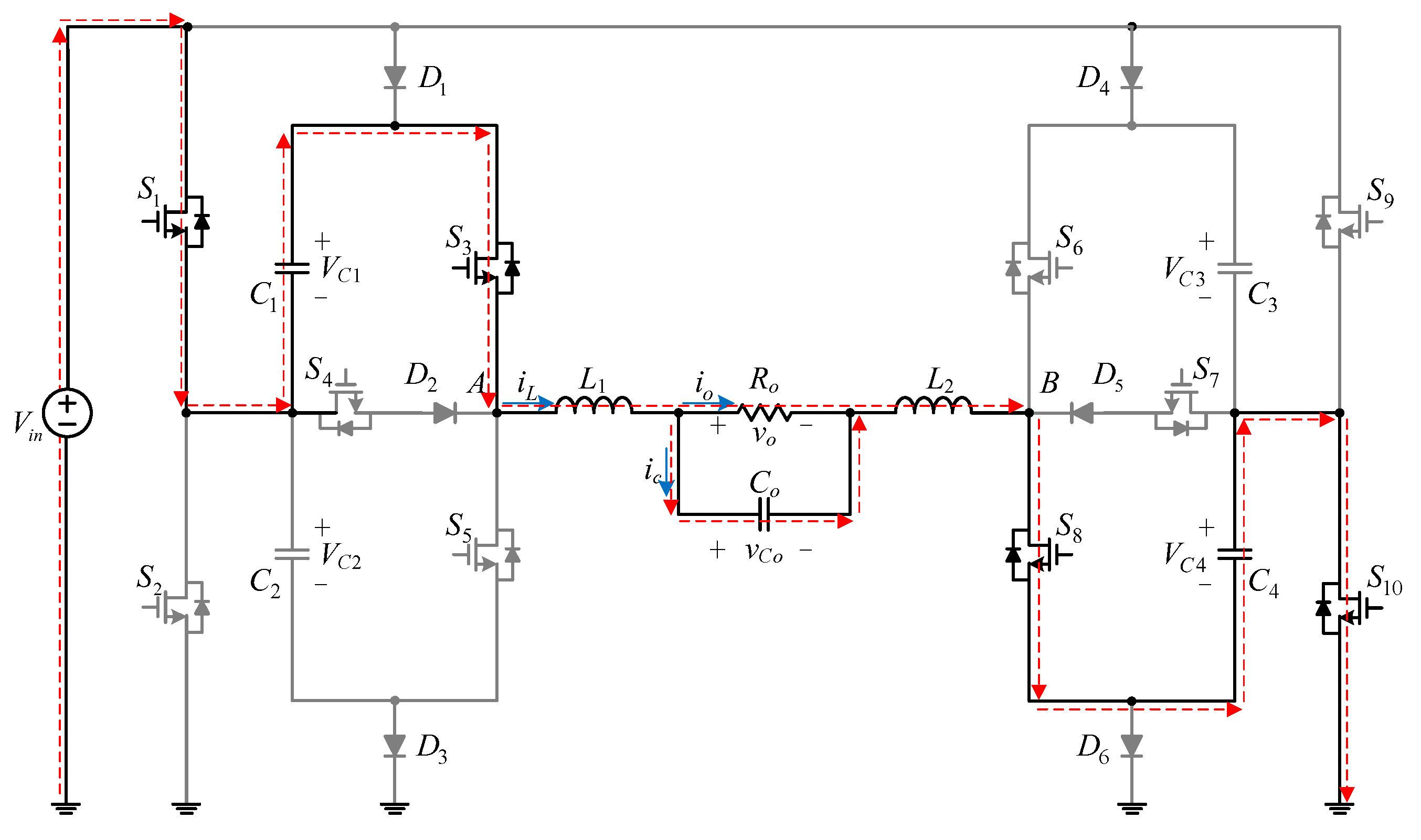
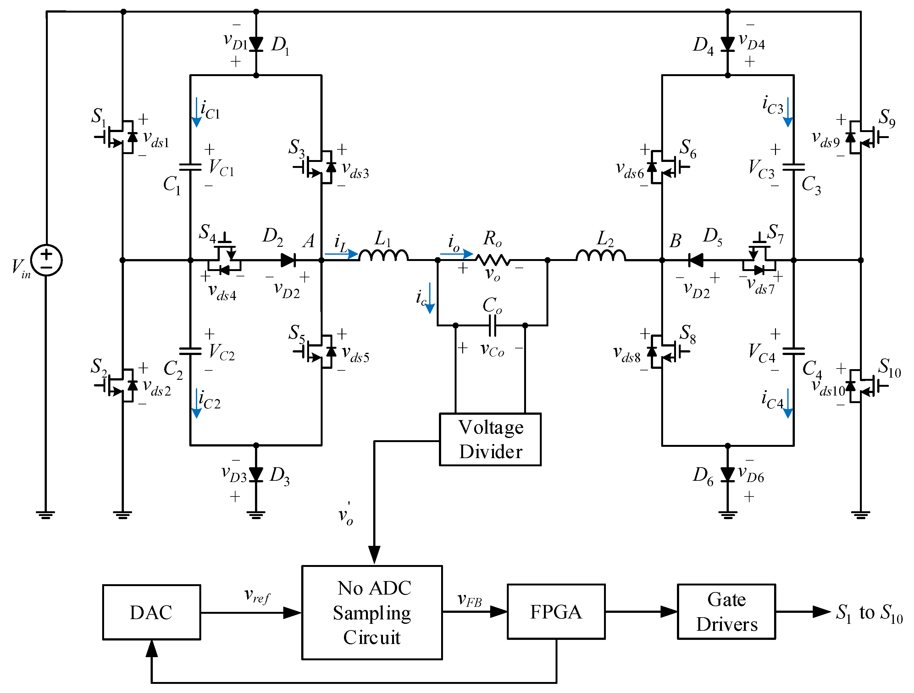
Figure 2a shows the proposed single-power-source T-type 7-level single-phase DC-AC inverter.
2.1. Operating Principle
Prior to the operation analysis, we will briefly explain the definition of the symbols and the assumptions required.
- (1)
- the input voltage is signified by Vin, the output voltage is denoted by vo, and the voltage across the output capacitor Co, VCo, is identical to vo.
- (2)
- the voltages on S1 to S10 are represented by vds1 to vds10, respectively.
- (3)
- the voltages on D1 to D6 are expressed by VD1 to VD6, respectively.
- (4)
- the currents in the energy-transferring capacitors C1 to C4 are denoted by iC1 to iC4, respectively.
- (5)
- It is assumed that the energy-transferring capacitances are large enough such that the voltages on the capacitors can be viewed as constant, i.e., VC1 = VC2 = VC3 = VC4.
- (6)
- the output current is signified by io, and the currents flowing through inductors L1 and L2 are expressed by iL.
- (7)
- All elements, except the body diodes of the switches, are considered as ideal.
Figure 2b displays the gate signals for the switches with level-shift sinusoidal pulse width modulation (LS-SPWM). As the gate signals at the positive half-cycle which are identical to those at the negative half-cycle, only the positive half-cycle is taken into consideration. There are five stages in circuit operation, and only one switch in each stage over one PWM switching cycle, while the rest of the switches are always on or off. Since stage I is identical to stage V and stage II is identical to stage IV, only stages I, II, and III are analyzed.
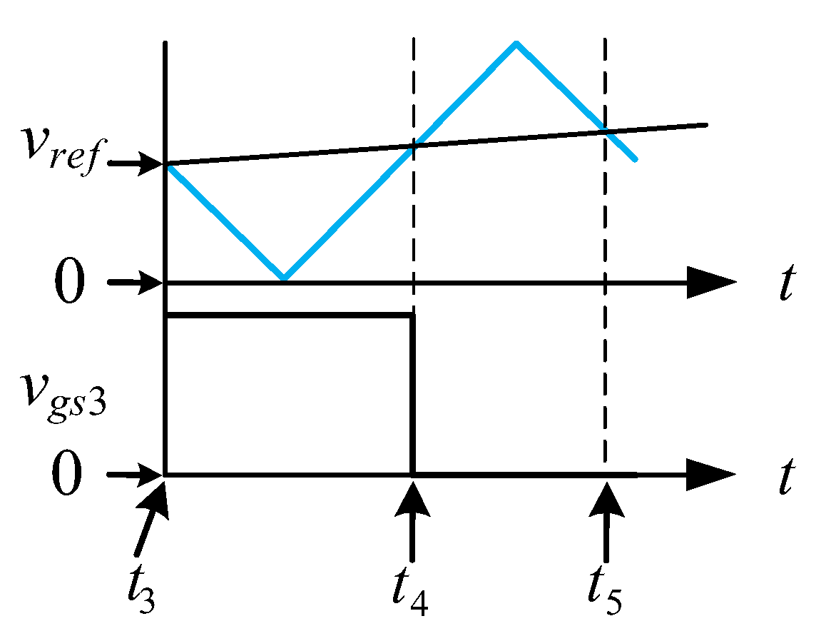
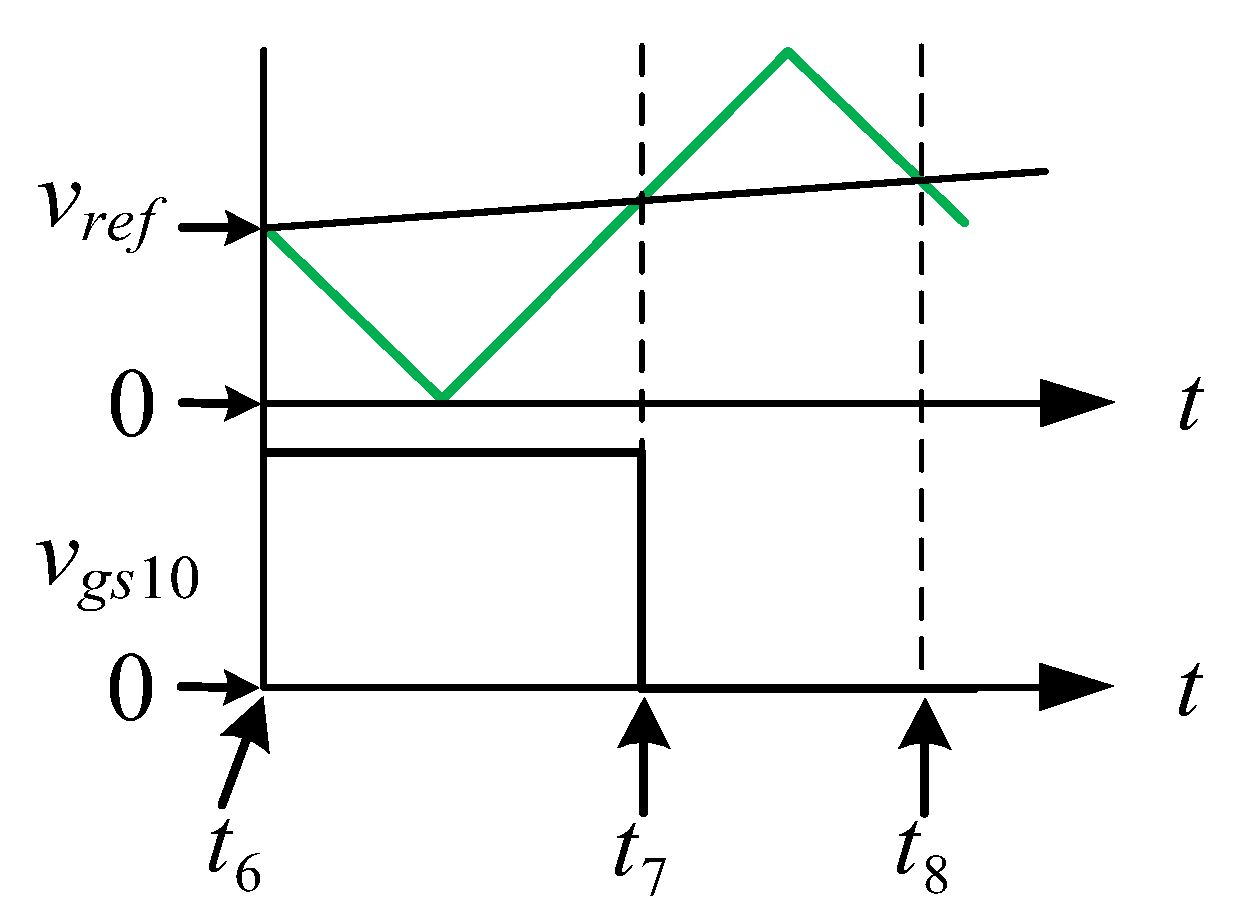
As the AC output voltage is at the positive half-cycle, the switches S1 and S8 are always in the on-state and the switches S2, S5, S6, S7, and S9 are always in the off-state. The output voltage will be obtained by switching S4, S3, and S10 to comply with the circuit operations of stages I, II, and III, respectively. To speak lucidly, all the three triangular waves are compared with the sinusoidal wave. If the latter is larger than the former, the turn-on times are generated. The red line is for vgs4, the blue line is for vgs3, and the green line is for vgs10.
2.1.1. Stage I
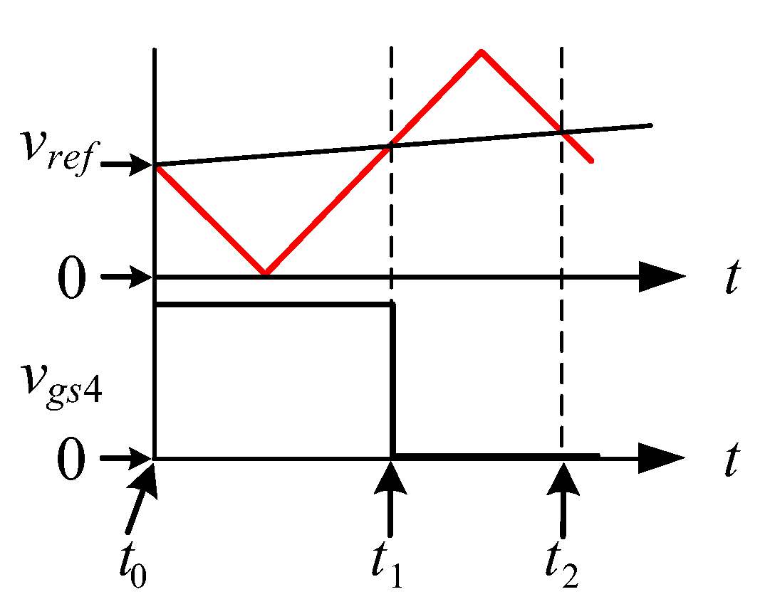
Only S4 is turned on/off as in Figure 3.
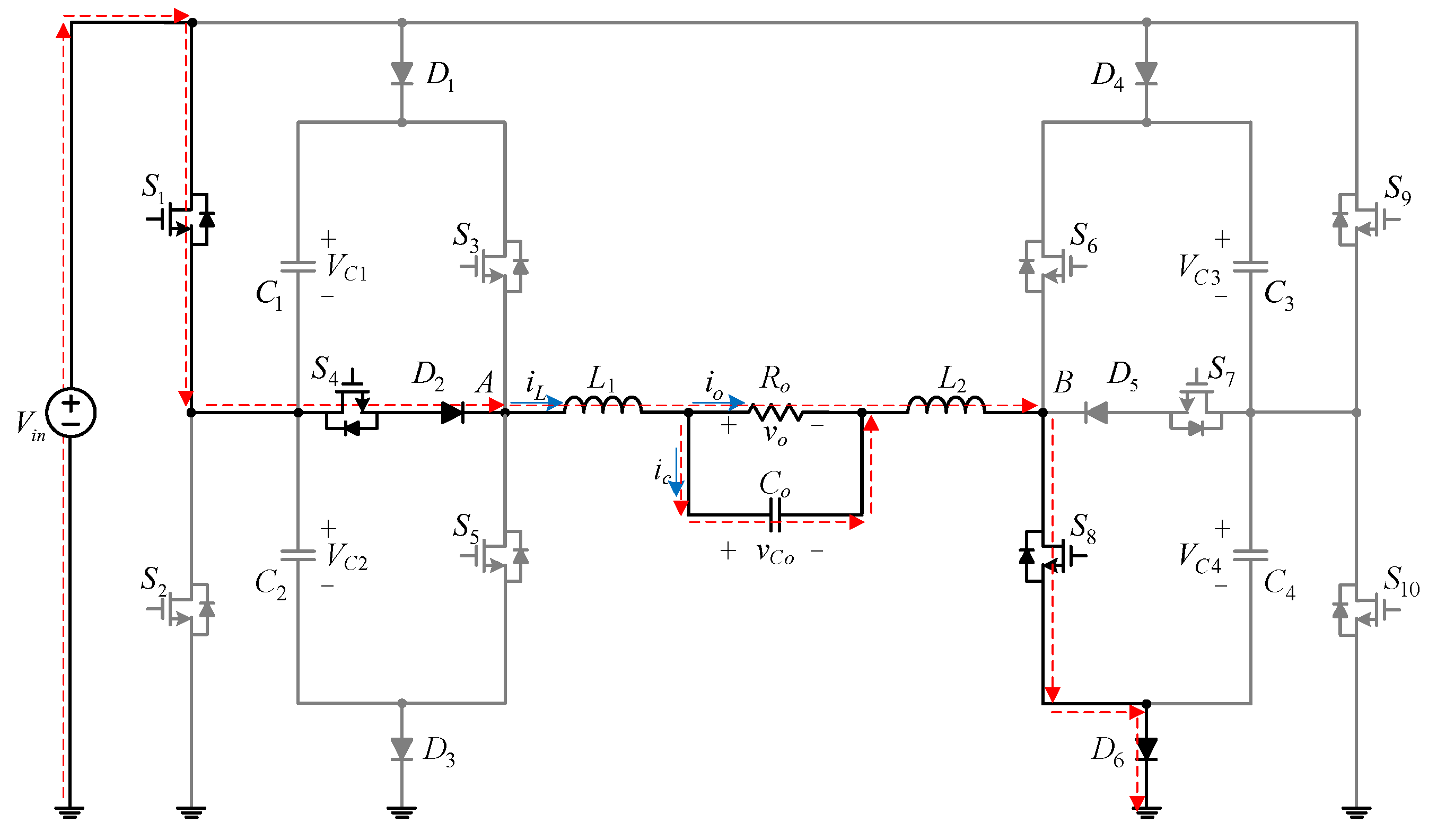
Time interval : As illustrated in Figure 2b and Figure 3, the switch S4 is on, but the switches S3 and S10 are off. As displayed in Figure 4, the power flow via the inductors L1 and L2 will generate a loop from the input voltage Vin to the switches S1, S4, S8 and the diodes D2, D6. Hence, the voltage across the terminals A and B, called vAB, is:
Time interval : As illustrated in Figure 2b and Figure 3, the switches S3, S4, and S10 are all off. As displayed in Figure 5, the power flow via the inductors L1 and L2 will generate a loop from the switches S1, S8, the diode D6, and the body diode of the switch S5. Hence, the voltage on the terminals A and B, named vAB, is:
2.1.2. Stage II
Only S3 is turned on/off as in Figure 6.
Time interval : As illustrated in Figure 2b and Figure 6, the switch S3 is on, but the switches S4 and S10 are off. Although the switch S4 is always in the on-state during this interval, the diode D2 is reverse biased so that no current passes through S4, which can be considered as equal to being in the off-state. As displayed in Figure 7, the power flow via the inductors L1 and L2 will generate a loop from the input voltage Vin to the switches S1, S3, S8, and the diode D6. Hence, the voltage on the terminals of A and B, called vAB, is:
Time interval : As illustrated in Figure 2b and Figure 6, the switches S3 and S10 are off, but the switch S4 is on. The power flow in this interval is the same as Figure 4. The power flow via the inductors L1 and L2 will generate a loop from the input voltage Vin to the switches S1, S4, S8, and the diodes D2 and D6. Hence, the voltage on the terminals A and B, named vAB, is Vin as shown in Equation (1).
2.1.3. Stage III
Only S10 is turned on/off as in Figure 8.
Time interval : As illustrated in Figure 2b and Figure 8, the switches S3 and S10 are on, but the switch S4 is off. As displayed in Figure 9, the current flow via the inductors L1 and L2 will generate a loop from the input voltage Vin to the switches S1, S3, S8, and S10. Hence, the voltage on the terminals of A and B, called vAB, is:
Time interval : As illustrated in Figure 2b and Figure 8, the switches S4 and S10 are cut off, but the switch S3 is on. The power flow in this interval is the same as Figure 7. The power flow via the inductors L1 and L2 will generate a loop from the input voltage Vin to the switches S1, S3, S8, and the diode D6. Hence, the voltage on the terminals A and B, named vAB, is 2Vin as shown in Equation (3).
According to the analysis mentioned above, the proposed 7-level DC-AC inverter possesses the voltage gain of 3, to be calculated based on (5):
2.2. Switch Behavior and Maximum Voltage Stress
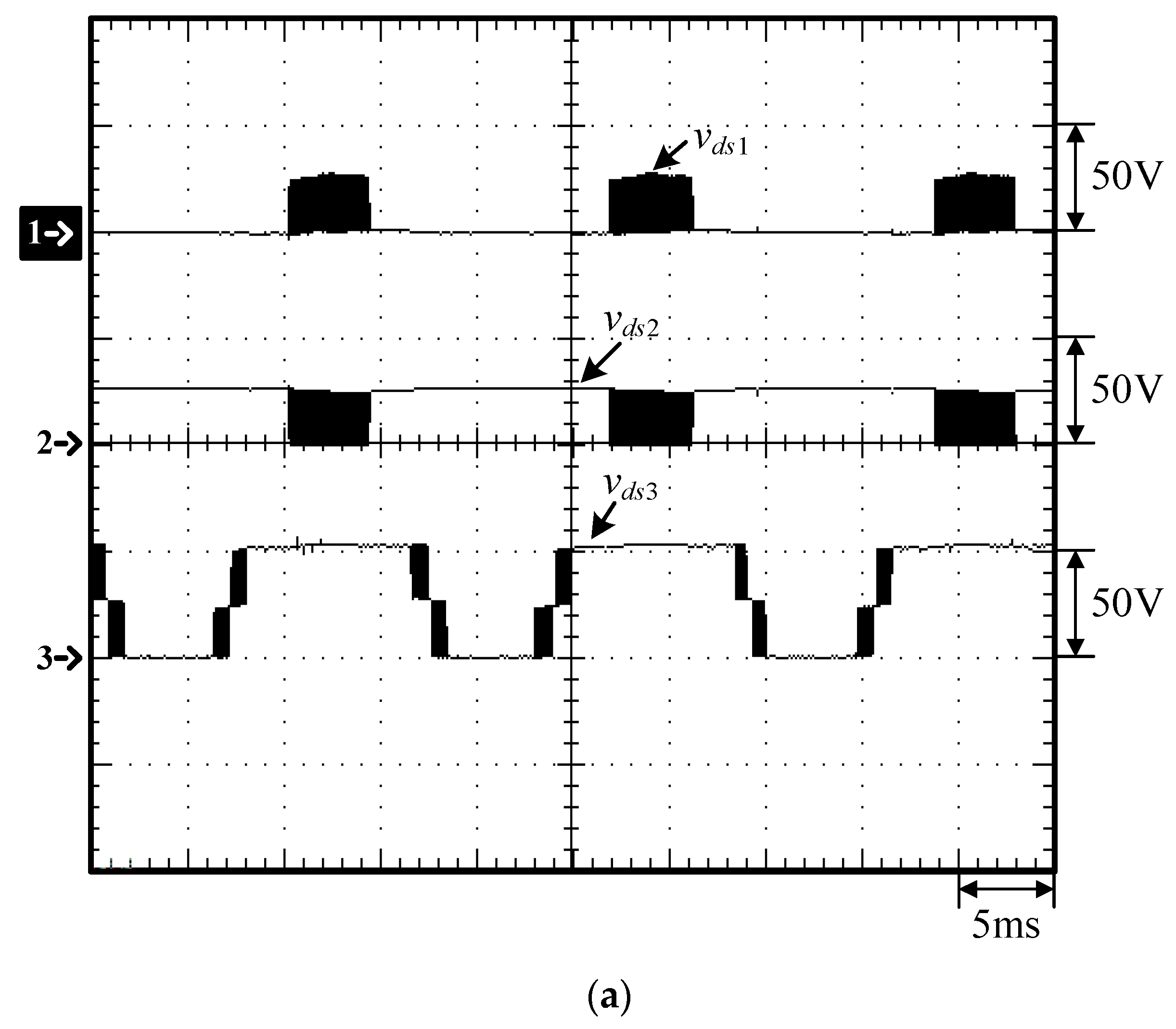
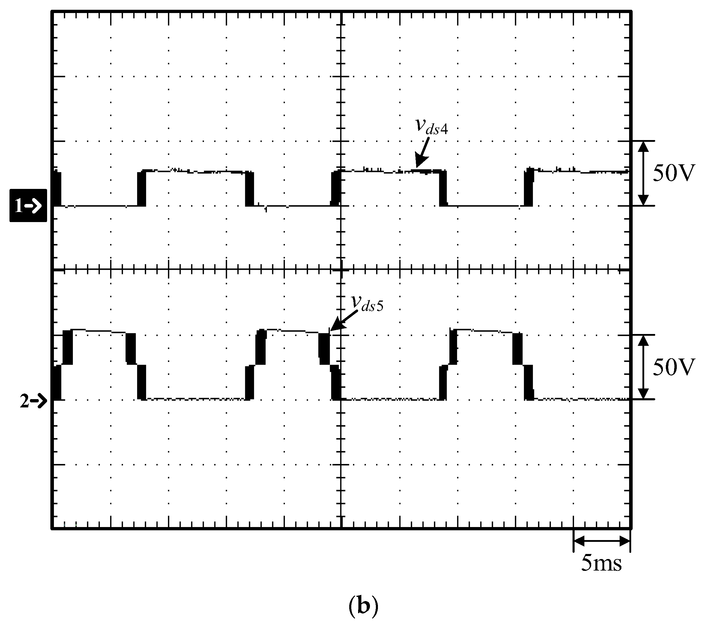
Table 2 displays the switch behavior of the proposed circuit and the corresponding maximum voltage stresses of switches, where fline is the mains frequency and fPWM is the switching frequency. Since the positive half-cycle is considered, the switches S2, S5, S6, S7, and S9 are kept off. The maximum voltage stress is Vin for all switches except for the switches S3 and S5, whose voltage stresses both are 2Vin.
3. Power Component Design
The specifications for the proposed DC-AC inverter are shown in Table 3.
3.1. Energy-Transferring Capacitor Design
The PSIM simulation results can be used to get the charge of two energy-transferring capacitors discharged at the positive half-cycle of the mains. By setting the voltage ripple rate at 10%, the capacitance can be obtained as below:
Consequently, for design convenience, a 3.3 mF electrolytic capacitor is used for each of the four energy-transferring capacitors, and the voltage across each capacitor is identical to the input voltage according to Section 2.1. Since the derating should be considered in use of the electrolytic capacitor, the voltage rating of the selected capacitor, based on thumb theorem, should be at least 1.25 times of the input voltage Vin, namely:
Eventually, the specifications of the selected capacitors are shown in Table 4.
3.2. Filter Design
The maximum total harmonic distortion is 5% under 69 kV or less [29], according to the harmonic voltage limit proposed by IEEE 519–1992. Since a multilevel DC-AC converter is operated at high frequencies, the output voltage contains high frequency components, leading to a total harmonic distortion greater than 5%. Consequently, a filter should be adopted to reduce the total harmonic distortion of the output voltage.
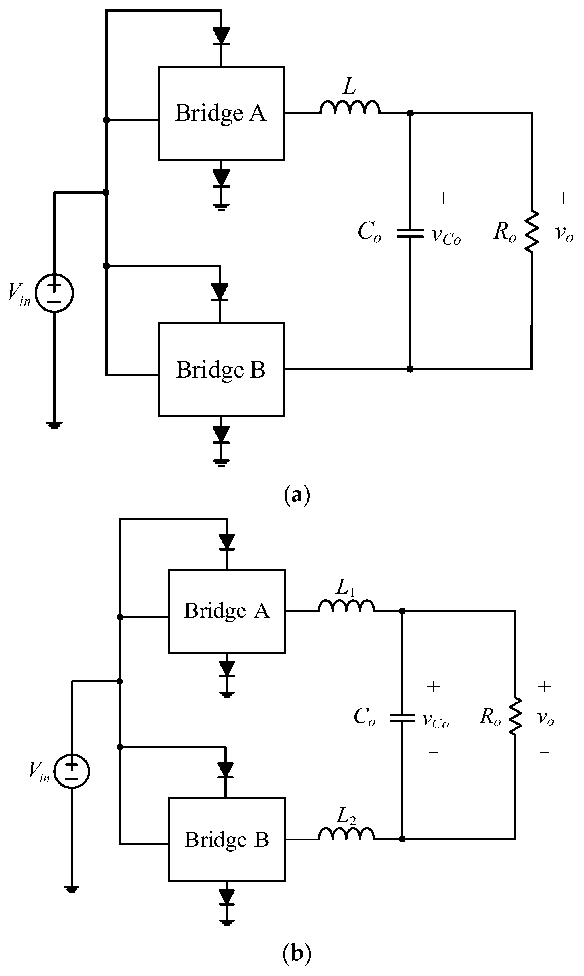
Since the proposed circuit has a double-ended symmetrical output, the inductance L of LC filter as shown in Figure 10a is divided into L1 and L2 as shown in Figure 10b, not only rendering the differential-mode (DM) noise to not exist at the output terminals, but also keeping the common-mode noise (CM) from influencing the operation of the circuit. Accordingly, L1 is connected with L2 in series as displayed in Figure 10b so let L be equal to the sum of L1 and L2 to do analysis and calculation, i.e., L = L1 + L2, where L1 = L2 = 0.5L.
High frequency switching is used to reduce the size of the filter, and the cut-off frequency fc of the filter is designed at 0.1 times the switching frequency fs to ensure that the fundamental and harmonics of the switching frequency can be filtered out by this filter. Since the switching frequency is prescribed at 60 kHz, the value of fc is prescribed at 6 kHz.
The transfer function of the filter, called F(s), is indicated in Equation (10) as follows:
In Equation (10), we can find the expressions of the cut-off frequency fc and the quality factor Q as below:
and:
Substituting the value of fc into Equation (11) yields:
At the same time, rearranging Equation (12) yields:
The value of Q at full load is set to 3 dB, that is , and substituting this value into Equation (14) yields:
Substituting Equation (15) into Equation (13) yields:
Substituting Equation (16) into Equation (15) yields:
One 1 μF/275 V metal film capacitor, manufactured by HJC Co., is selected as Co.
Therefore, the value of the individual values of L1 and L2 can be chosen to be:
Eventually, the individual values of L1 and L2 are selected as 367 μH.
Two low permeability cores are selected for cores of L1 and L2 along with the following parameters shown in Table 5.
Since the inductors L1 and L2 are the same, whose values are 367 μH, the required number of turns N, wound on the T106-26 core, is:
Eventually, each inductance is 375 μH with 55 turns.
On the other hand, the current density Jf is designed to be 400 A/cm2, and by considering the skin effect and using a wire diameter Φf of 0.5 mm, the required number of strands is:
According to the result of Equation (20), 4 wires of 0.5 mm diameter enameled wire are wound on the used cores to obtain the filter inductors L1 and L2.
In addition, the product name for S1, S2, S4, S7, S9, and S10 is AP75T45GP-HF, while the product name for S3, S5, S6, and S8 is IPP076N15N5. The product name for D1 to D6 is SBR20A100CTFP.
4. Modeling and Controller Design
4.1. Modeling
4.1.1. Small-Signal Analysis of Stage I
The state-space equations of the circuit are shown in Equation (21) and Equation (22) as the switch S4 is turned on and off, respectively, during stage I:
Based on the state-space averaging method [26], it is assumed that the switch S4 is on during the period of dTs and the switch S4 is off during the period of (1−d)Ts, where d is duty cycle and Ts is the switching period. After this, by multiplying Equation (21) by dTs and Equation (22) by (1−d)Ts, the state-space averaging equations of stage I, via summing these two corresponding results, can be obtained to be:
Since each parameter of the converter contains a DC quiescent operating point and an AC small signal, we can express the corresponding parameters as shown in Equation (24):
Substituting Equation (24) into Equation (23) yields the small-signal AC model equation:
4.1.2. Small-Signal Analysis of Stage II
The state-space equations of the circuit are shown in Equation (26) and Equation (21) as the switch S3 is turned on and off, respectively, during stage II:
where according to the analysis in Section 2, the voltage across the energy-transferring capacitor C1 is treated as the input voltage, i.e., vC1 = vin.
Sequentially, it is assumed that the switch S3 is on during the period of dTs and the switch S3 is off during the period of (1 − d)Ts. Afterwards, by multiplying Equation (26) by dTs and (21) by (1 − d)Ts, the state-space averaging equations of stage II, via summing these two corresponding results, can be obtained to be:
Substituting Equation (24) into Equation (27) yields the small-signal AC model equation, which is the same as Equation (25).
4.1.3. Small-Signal Analysis of Stage III
The state-space equations of the circuit are shown in Equation (28) and Equation (26) as the switch S10 is turned on and off, respectively, during stage III:
where according to the analysis in Section 2, the voltage across the energy-transferring capacitors C1 and C4 are treated as the input voltage, i.e., vC1 = vC4 = vin.
Sequentially, it is assumed that the switch S10 is on during the period of dTs and the switch S10 is off during the period of (1 − d)Ts. After this, by multiplying Equation (28) by dTs and Equation (26) by (1 − d)Ts, the state-space averaging equations of stage III, via summing these two corresponding results, can be obtained to be:
Substituting Equation (24) into Equation (29) yields the small-signal AC equation, which is the same as Equation (25).
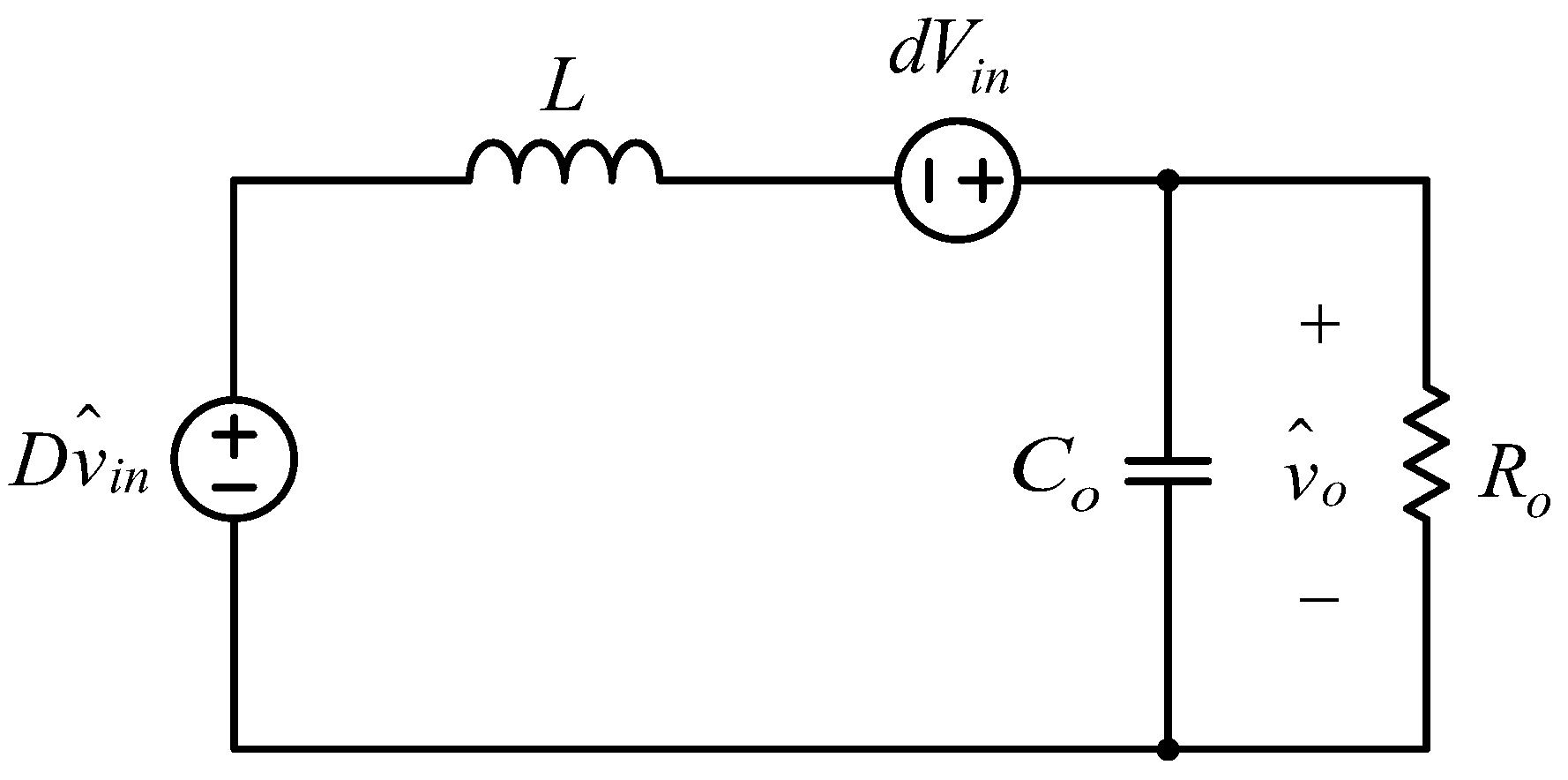
From above analysis, it can be seen that the small-signal ac model of the proposed inverter is the same for any stage, and it is shown in Figure 11. From this figure, it can be seen that the small-signal AC model of the proposed inverter is the same as that of the conventional DC-DC buck converter. As a result, the control design can be carried out easily and systematically.
4.2. Controller Design
First, taking the Laplace transform of the circuit shown in Figure 11 yields the control-force-to-output-voltage transfer function Gvd(s):
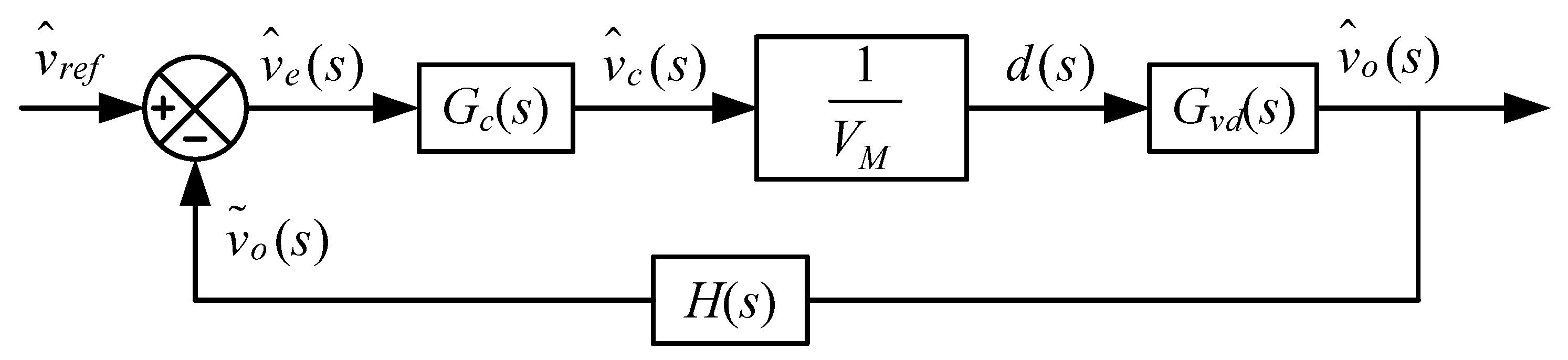
Accordingly, the system block diagram for voltage feedback control of the proposed circuit can be obtained as shown in Figure 12, where Gc(s) represents the controller transfer function, VM denotes the peak-to-peak triangular wave transfer function, and H(s) signifies the voltage divider transfer function. The loop gain T(s) is equal to .
First, let and , the phase angle at the crossover radian frequency is calculated by MATLAB to be approximately , and based on the radian frequency compensation parameter table as described in [30] and the designed values of components as shown in Section 3, can be obtained to be:
In general, the general system stability condition is set at the compensation phase between and , so the compensation phase is set at to calculate the required angle after compensation as follows:
Substituting the phase calculated by Equation (32) into the formula of the proportional gain kp shown in Equation (33) and the integral gain ki shown in Equation (34) to find their corresponding values as below:
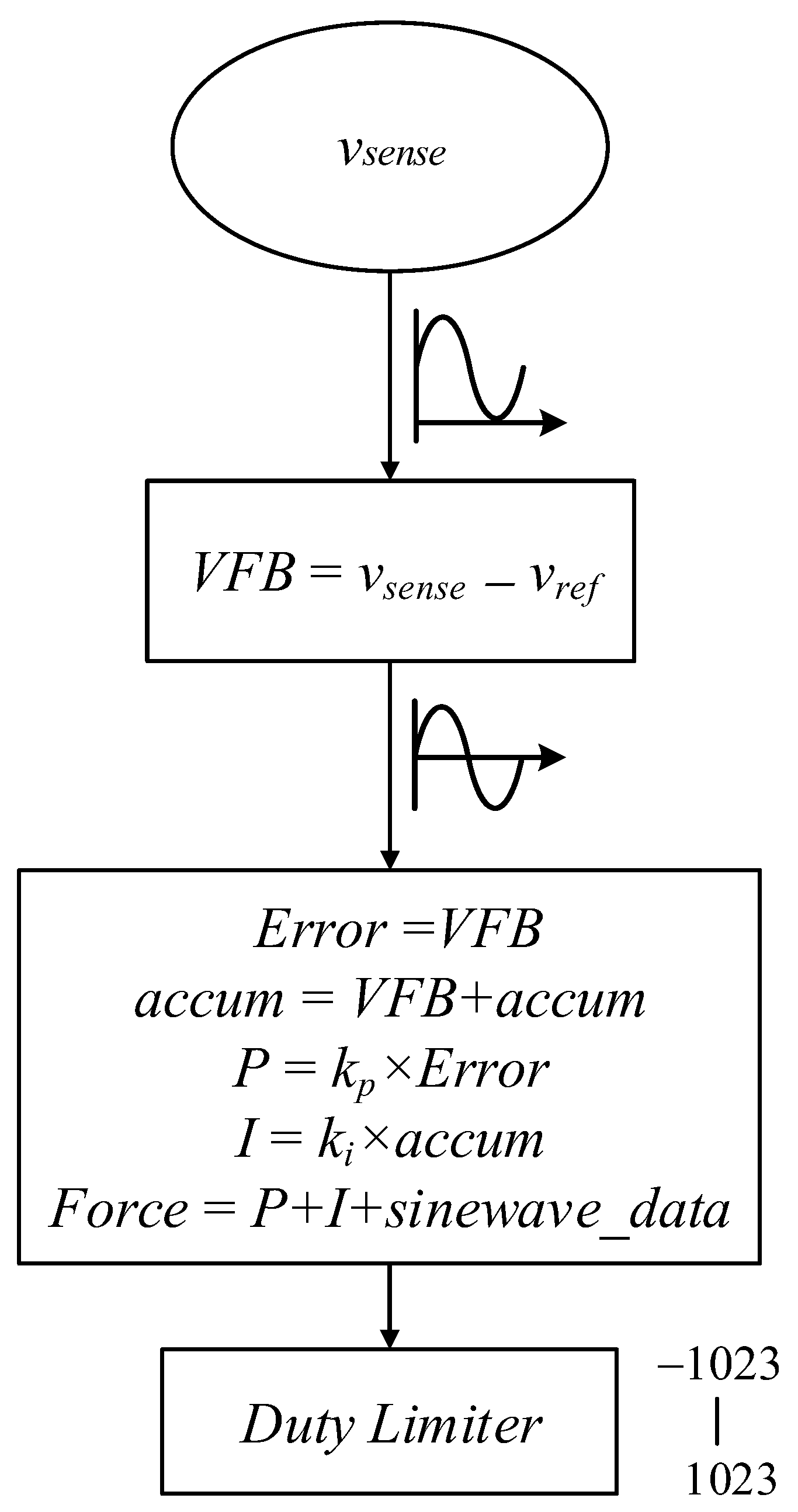
Figure 13 shows the control flow chart. The signal vsense is after no analog-to-digital converter (ADC) sampling so it is a digital value. This value is positive and is subtracted from the reference value vref to get VFB, which is a positive/negative number. Afterwards, set the variable Error to store the current error value and multiply it by the coefficient kp to get the proportional control force P. At the same time, set the variable accum to store the cumulative value, and each operation will add the previous error value to this operation, then multiply this variable by the coefficient ki to get the integral control force I. Finally, add P, I, and the digital sine wave signal, called sinewave_data, to get the control force, called Force, which is restricted by a limiter, called Duty Limiter, between −1023 and 1023.
5. Results and Discussion
5.1. System Configuration
Figure 14 shows the system configuration for the proposed 7-level single-phase DC-AC inverter. This system is built up by the main circuit and the feedback circuit. The field-programmable gate array (FPGA) and digital-to-analog converter (DAC) are used to create sinusoidal voltage reference signal vref, and no ADC sampling circuit is used to transmit the feedback signal vFB to the FPGA to get the resulting control effort after calculation. This control effort is then sent to the isolated gate driver to make the switch on/off to achieve a desired output voltage.
5.2. Simulation and Experiment with Discussion
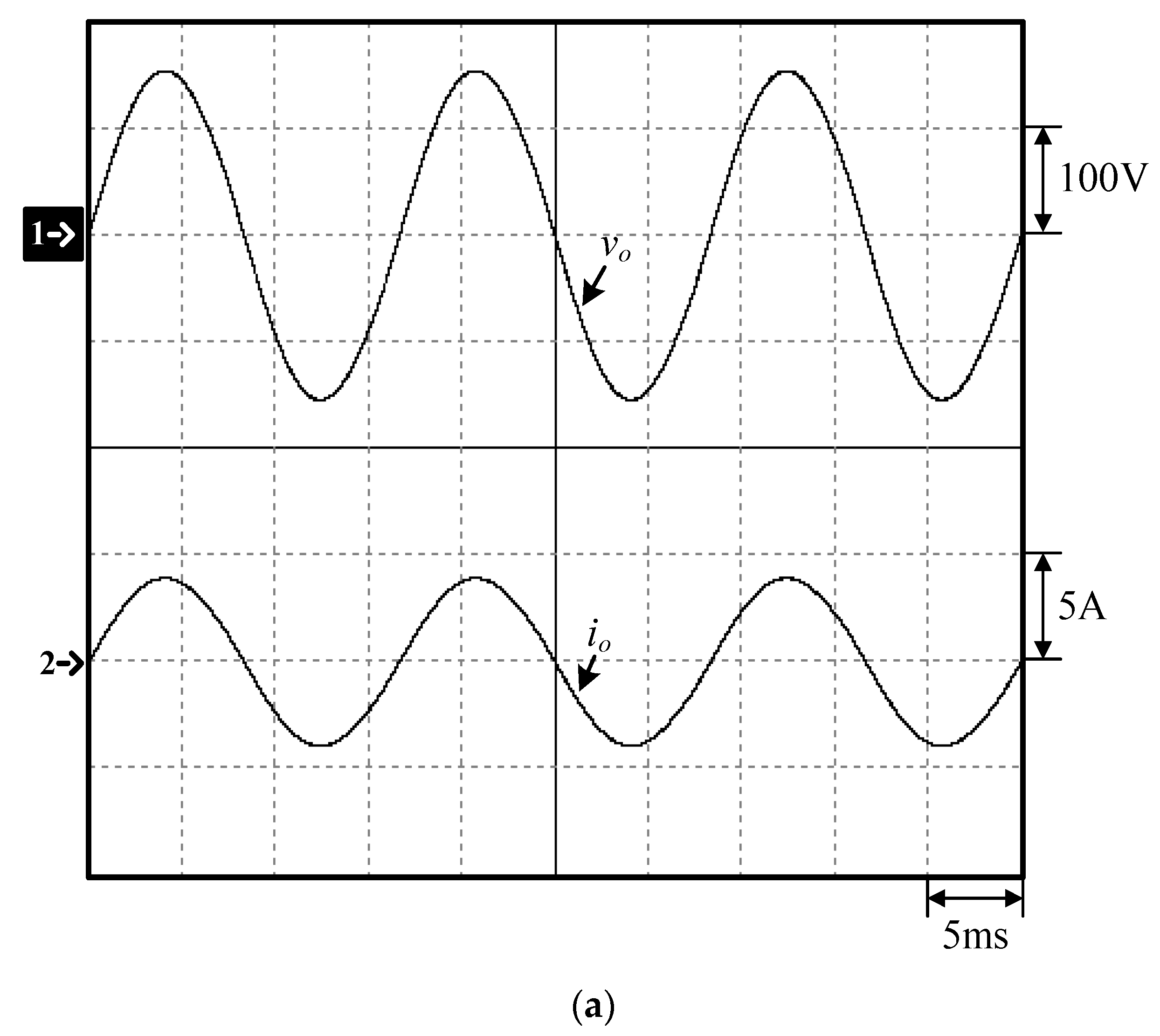
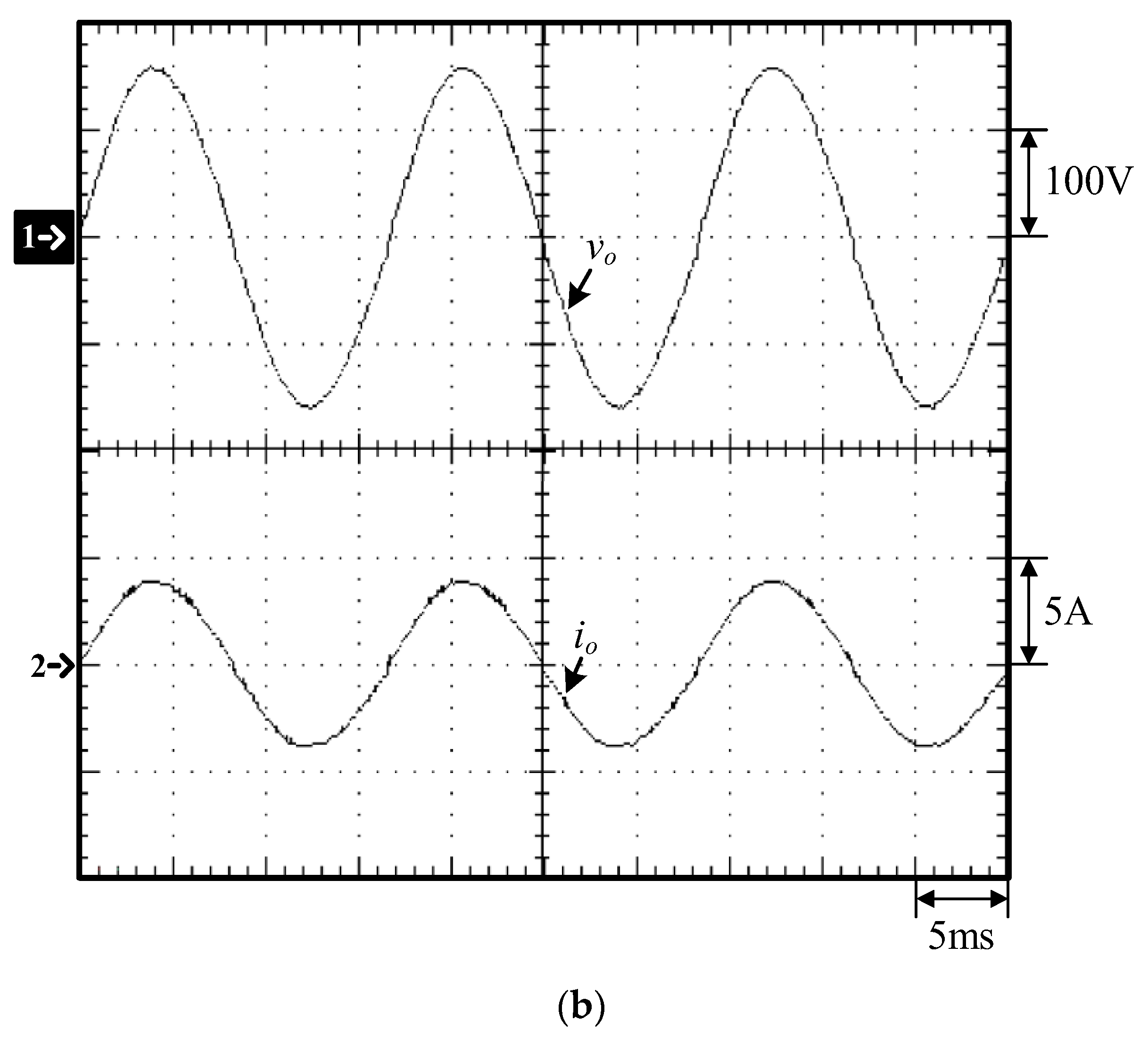
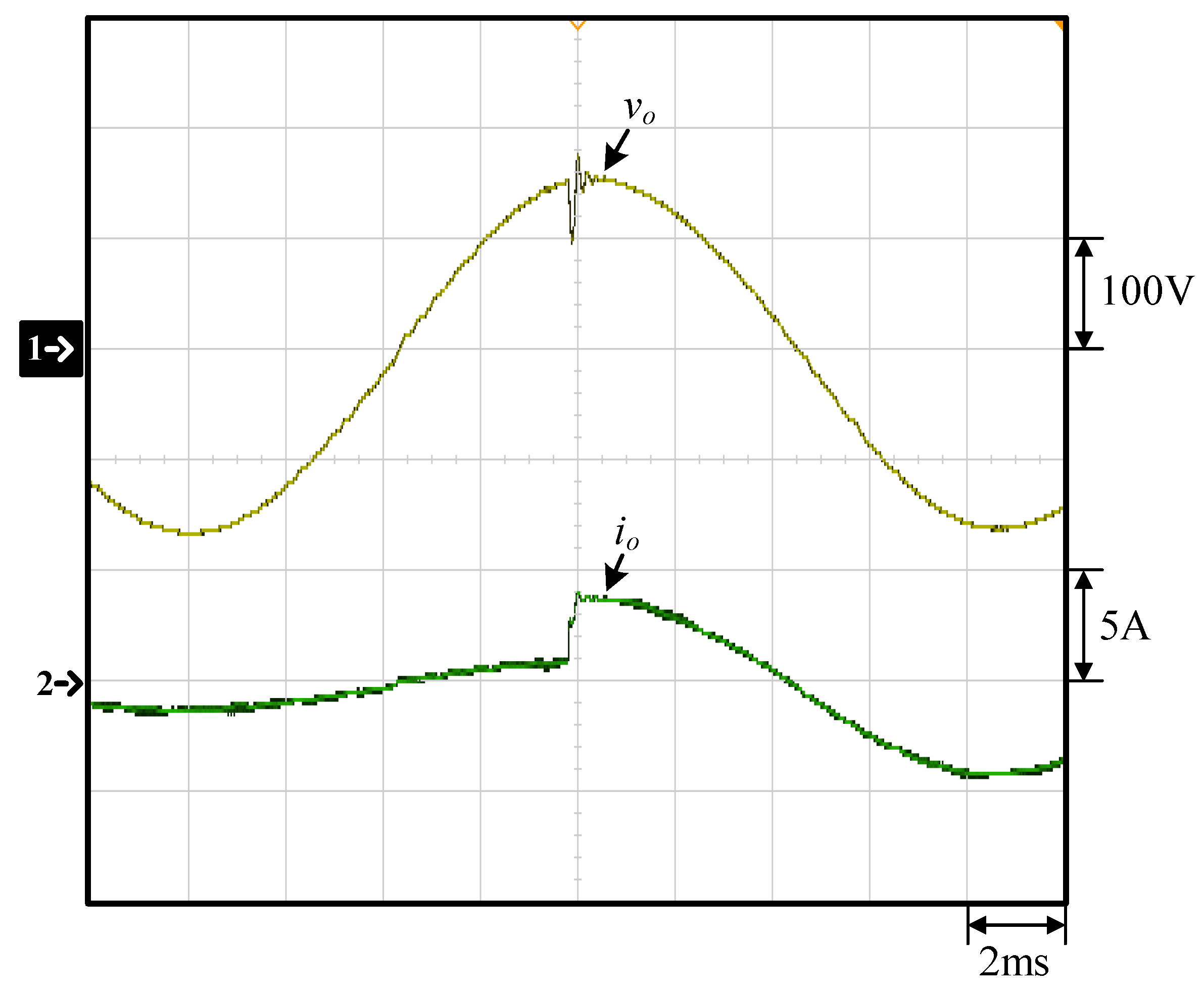
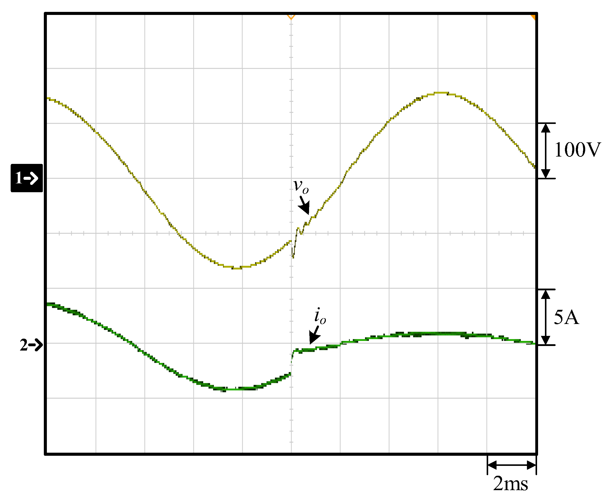
Under closed loop at rated load, Figure 15 shows the output voltage vo and current io. Figure 16 displays the output voltage vo and the unfiltered output voltage vPWM. Figure 17 and Figure 18 show the voltages on the energy-transferring capacitors C1, C2, C3, and C4. Figure 19 only shows the voltage stresses on the switches S1 to S5 due to the circuit symmetry. Figure 20 and Figure 21 display the upload and download transient responses based on load variations from 25% to 100% load and from 100% to 25% load, respectively.
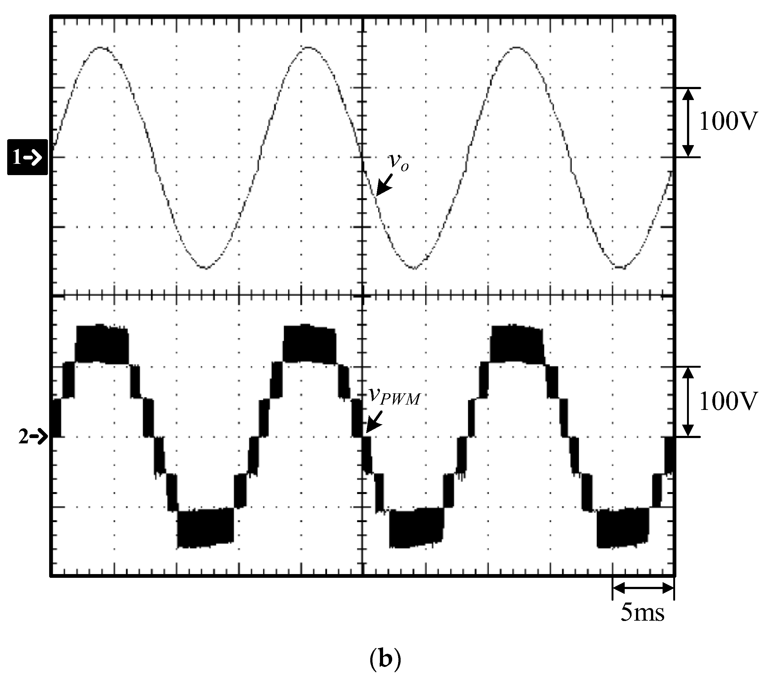
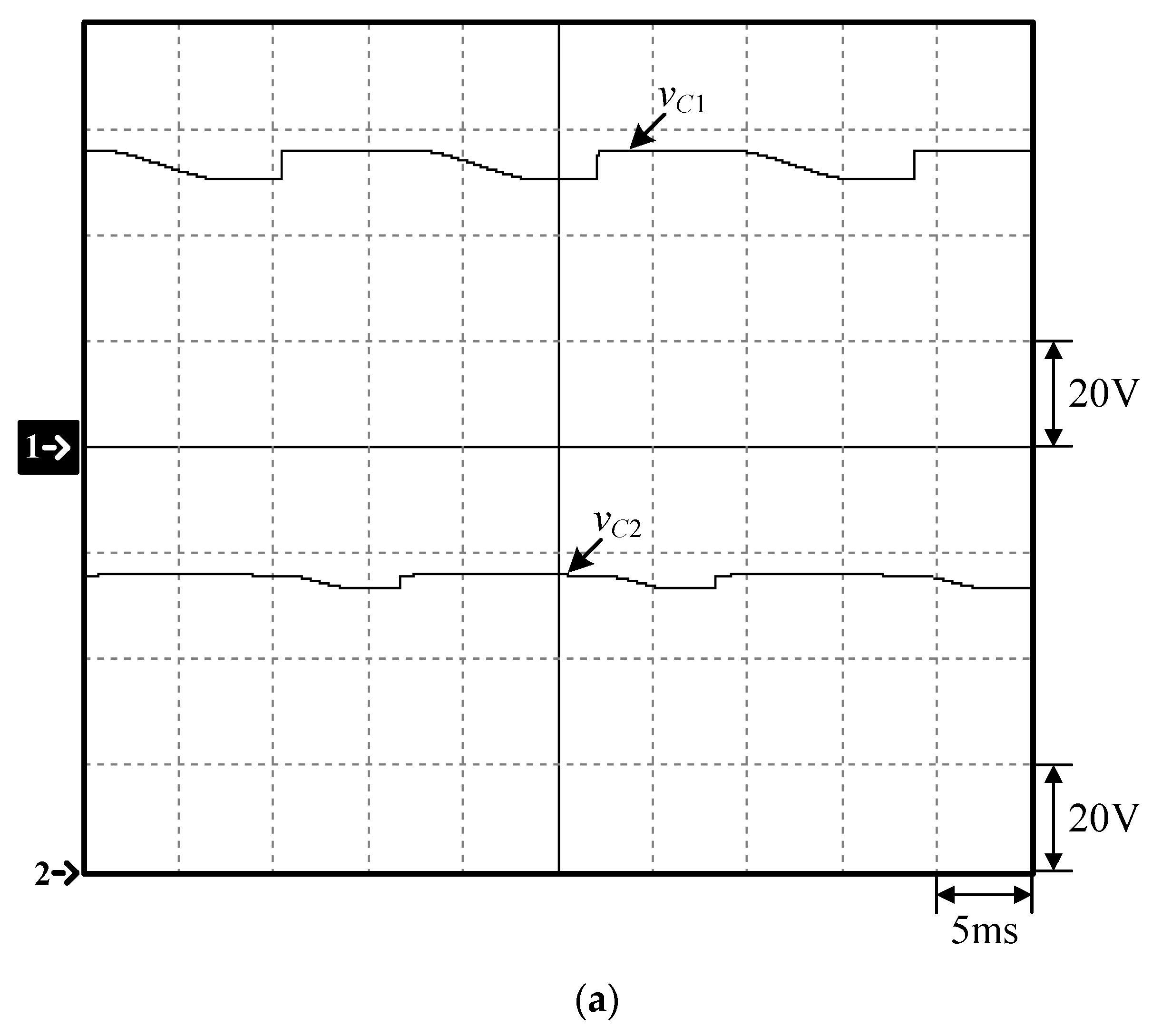
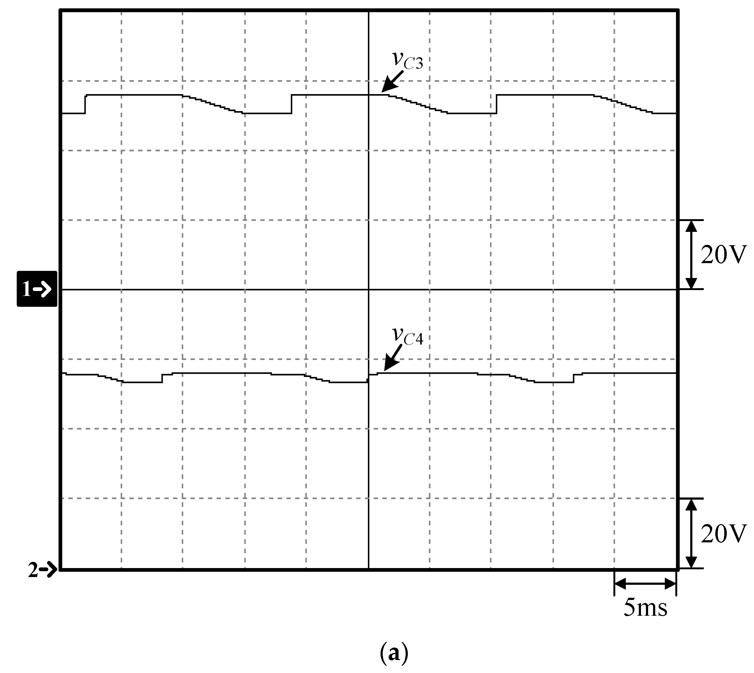
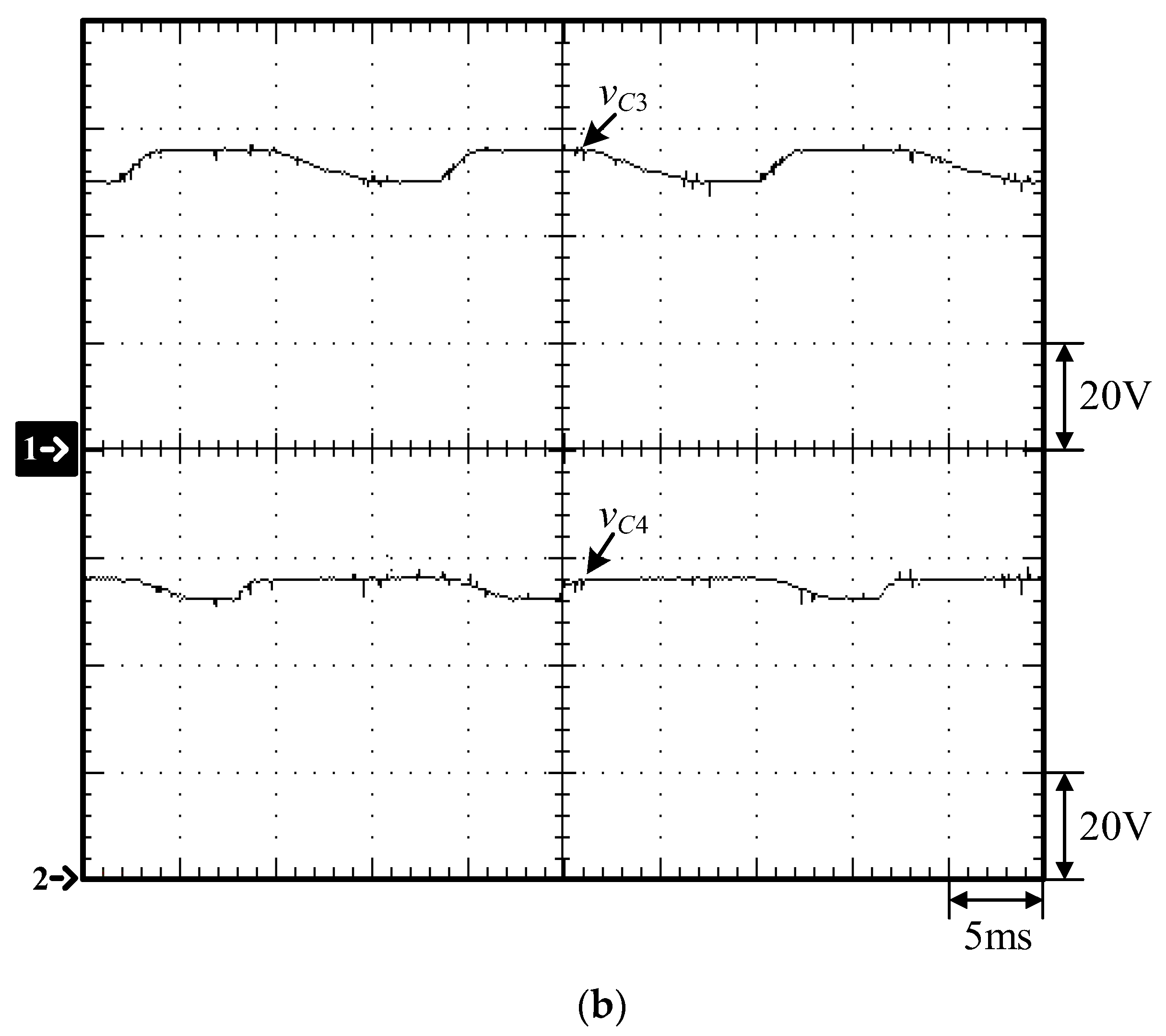
From Figure 15, it can be seen that the output voltage vo and output current io are both AC outputs. From Figure 16, it can be seen that the unfiltered output voltage vPWM possesses 7 levels generated by the gate signal with high switching frequency to conduct and cut off the switch and is filtered to get 60 Hz AC voltage with voltage gain of 3. As can be seen from Figure 17 and Figure 18, the energy-transferring capacitors possess self-balancing. From Figure 19, it can be seen that all switches have voltage stresses of the input voltage except the switches S3 and S5, whose voltage stresses are double the input voltage. From Figure 20 and Figure 21, it can be seen that the former has an undershoot voltage of about 50 V and a recovery time of about 0.6 ms, and the latter has an overshoot voltage of about 45 V and a recovery time of about 1.5 ms. From the above simulated and measured results, it is obvious that good agreement between the simulated and experimental results validates the feasibility and effectiveness of the proposed single-power-source T-type 7-level single-phase DC-AC inverter.
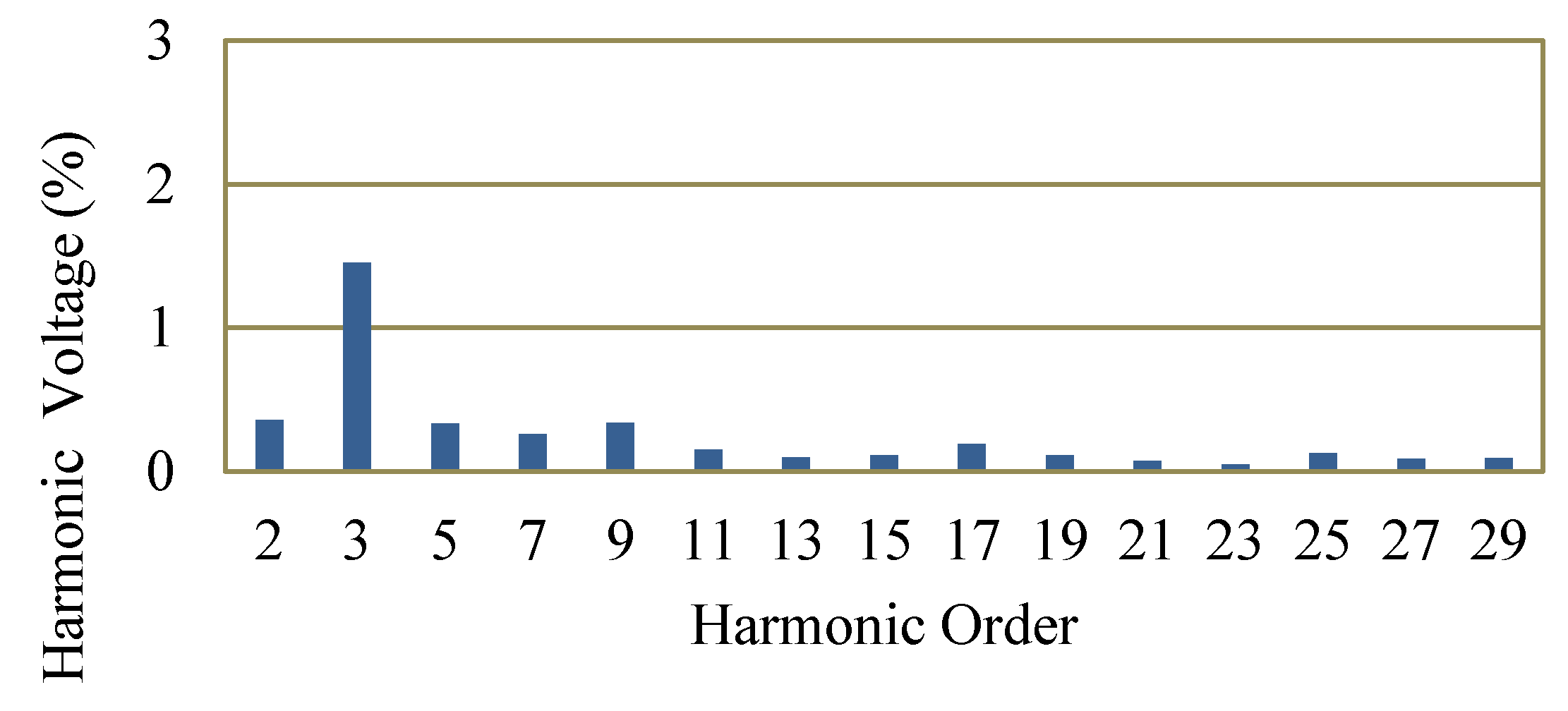
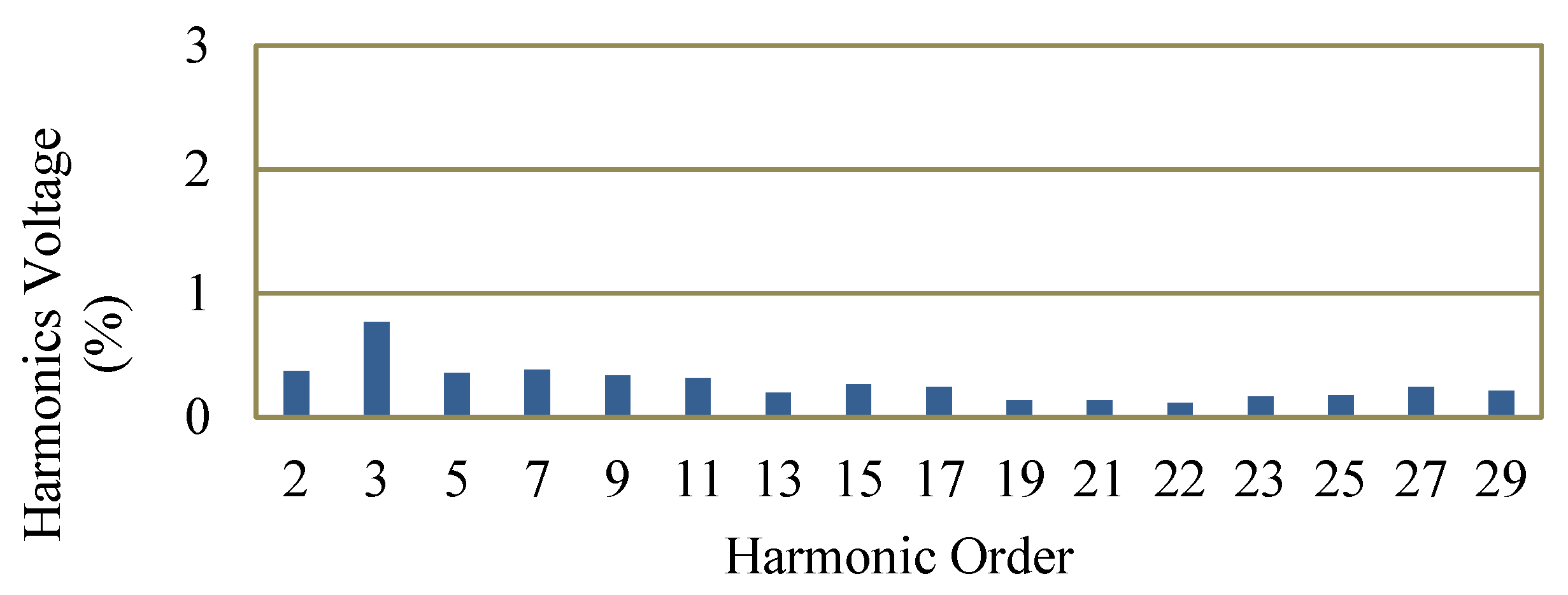
5.3. Voltage Harmonic Distribution
Figure 22 and Figure 23 show the voltage harmonic distribution at 100% and 25% load, respectively. The total harmonic distortion (THD) of the output voltage of the single source T-type 7-phase DC-AC inverter at 100% load and 25% load are 2.01% and 3.36%, respectively, which are small enough to remove or downsize the output filter, leading to less volume and cost. Furthermore, the proposed DC-AC inverter can indeed meet the IEEE 519–1992 requirement of less than 5% THD of voltage harmonics.
5.4. Efficiency Measurement
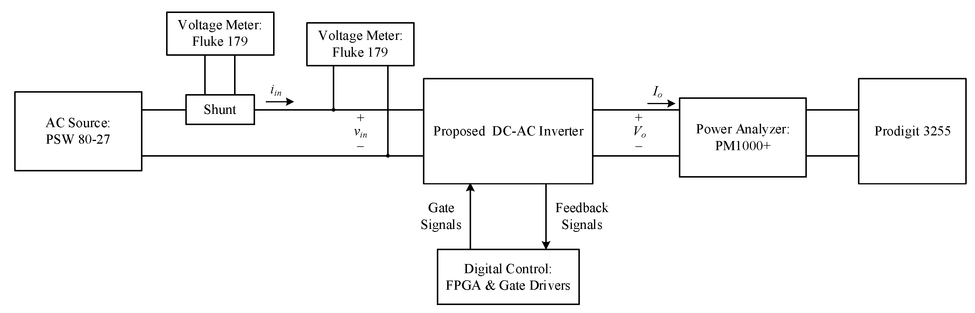
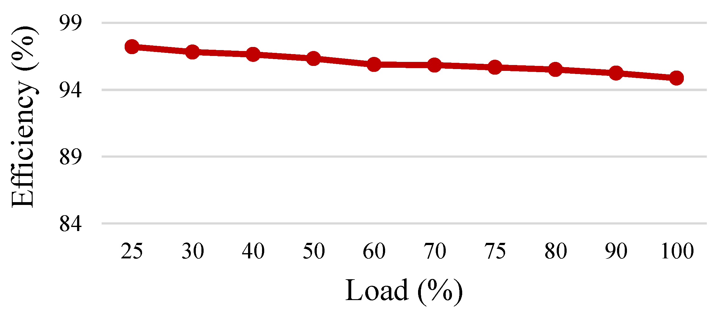
The efficiency of the proposed inverter circuit at various loads is measured as shown in Figure 24. First of all, a digital meter (Fluke 179) is used to measure the input voltage and the voltage on a current-sensing resistor (Shunt) to obtain the input current. Sequentially, the output voltage and current, total harmonic distortion, and harmonics of each number are measured by utilizing a power analyzer (PM1000+). Afterwards, the input and output powers can be obtained. Moreover, an AC electronic load (Prodigit 3255) is adopted at the load side. Eventually, the resulting input and output powers are employed to calculate the overall efficiency as illustrated in Figure 25. From this figure, it can be seen that the proposed inverter is based on the T-type circuit, thereby making the efficiency reduced as load is increased. The efficiency all over the load range is above 94% and the maximum efficiency is 97.42%.
5.5. Comparison between Proposed Inverter and Other Topologies
6. Conclusions
The proposed inverter has the following features as described below:
- This circuit has a symmetrical structure possessing voltage gain of 3 and self-balancing along with low THD. As a result, the mass production interchangeability can be obtained easily.
- Only one switch operates at any time, and not only is the corresponding control quite easy, but also any switch has very low switching losses and voltage stress.
- Since the mathematical model of the multilevel DC-AC inverter is successfully developed using the state-space averaging method, the voltage controller for the multilevel DC-AC inverter can be designed systematically and easily.
Furthermore, since the proposed DC-AC inverter possesses low THD, the possible applications of the proposed inverter in the industry are mentioned below:
- It can be applied to a single AC motor to reduce the torque ripple.
- It can be also applied to the low-frequency transformer to reduce the core loss.
- It can be applied to utility parallel of green power with relatively low electric pollution.
However, two switches have the maximum voltage stress of double input voltage. Consequently, this should be considered in practical perspective.
In addition, the possible developments of the proposed inverter in this research activity are mentioned below:
- Many researchers have focused on the structure and output of the multilevel inverter, but comparatively few researchers on the THD and product usefulness. Accordingly, THD reduction and circuit symmetry should be investigated.
- In general, only open-loop steady-state waveforms are shown in many papers. That is, dynamic responses are not considered. Accordingly, modeling of the multilevel inverter and closed-loop controller design should be developed.
- Up to now, there is no standard of the input voltage. Accordingly, by taking 12 V as a base, a multiple of this base to get 24 V, 48 V, and 96 V makes the user commonality achieved.
Author Contributions
Conceptualization, J.-J.S., K.-I.H. and Y.-Y.L.; methodology, J.-J.S.; software, Y.-Y.L.; validation, Y.-Y.L., K.-I.H. and J.-J.S.; formal analysis, Y.-Y.L.; investigation, J.-J.S.; resources, Y.-Y.L.; data curation, J.-J.S.; writing—original draft preparation, K.-I.H.; writing—review and editing, K.-I.H.; visualization, J.-J.S.; supervision, K.-I.H.; project administration, K.-I.H.; funding acquisition, K.-I.H. All authors have read and agreed to the published version of the manuscript.
Funding
This research was funded by the Ministry of Science and Technology, Taiwan, under the Grant Number: MOST 110-2221-E-027-045-MY2.
Data Availability Statement
No new data were generated or analyzed in this study. Sharing of the data in this article is not applicable.
Conflicts of Interest
The authors declare no conflict of interest.
References
- Wang, Y.; Shi, W.W.; Xie, N.; Wang, C.M. Diode-free T-type three-level neutral-point-clamped inverter for low-voltage renewable energy system. IEEE Trans. Ind. Electron. 2014, 61, 6168–6174. [Google Scholar] [CrossRef]
- Wu, F.; Li, X.; Feng, F.; Gooi, H.B. Modified cascaded multilevel grid-connected inverter to enhance European efficiency and several extended topologies. IEEE Trans. Ind. Inform. 2015, 11, 1358–1365. [Google Scholar] [CrossRef]
- Benedetti, D.; Agnelli, J.; Gagliardi, A.; Dini, P.; Saponara, S. Design of an off-grid photovoltaic carport for a full electric vehicle recharging. In Proceedings of the IEEE EEEIC/I&CPS Europe’20, Madrid, Spain, 9–12 June 2020; pp. 1–6. [Google Scholar]
- Dini, P.; Saponara, S. Electro-thermal model-based design of bidirectional on-board chargers in hybrid and full electric vehicles. Electronics 2022, 11, 112. [Google Scholar] [CrossRef]
- Rasool, H.; Verbrugge, B.; Zhaksylyk, A.; Tran, T.M.; El Baghdadi, M.; Geury, T.; Hegazy, O. Design optimization and electro-thermal modeling of an off-board charging system for electric bus applications. IEEE Access 2021, 9, 84501–84519. [Google Scholar] [CrossRef]
- Dhanamjayulu, C.; Khasim, S.R.; Padmanaban, S.; Arunkumar, G.; Holm-Nielsen, J.B.; Blaabjerg, F. Design and implementation of multilevel inverters for fuel cell energy conversion system. IEEE Access 2020, 8, 183690–183707. [Google Scholar] [CrossRef]
- Ardashir, J.F.; Sabahi, M.; Hosseini, S.H.; Blaabjerg, F.; Babaei, E.; Gharehpetian, G.B. A single-phase transformerless inverter with charge pump circuit concept for grid-tied PV applications. IEEE Trans. Ind. Electron. 2017, 64, 5403–5415. [Google Scholar] [CrossRef]
- Sen, P.; Jha, V.; Sahoo, A.K. Inrush current minimization in reduced device count multilevel inverter interfacing PV system. In Proceedings of the IEEE International Conference on Energy, Power and Environment: Towards Clean Energy Technologies, Bucharest, Romania, 13–14 October 2021; pp. 1–6. [Google Scholar]
- Malinowski, M.; Gopakumar, K.; Rodriguez, J.; Perez, M.A. A survey on cascaded multilevel inverters. IEEE Trans. Ind. Electron. 2010, 57, 2197–2206. [Google Scholar] [CrossRef]
- Lee, S.S.; Bak, Y.; Kim, S.-M.; Joseph, A.; Lee, K.-B. New family of boost switched-capacitor seven-level inverters (BSC7LI). IEEE Trans. Power Electron. 2019, 34, 10471–10479. [Google Scholar] [CrossRef]
- Ali, J.S.M.; Krishnasamy, V. Compact switched capacitor multilevel inverter (CSCMLI) with self-voltage balancing and boosting ability. IEEE Trans. Power Electron. 2019, 34, 4009–4013. [Google Scholar]
- Siddique, M.D.; Mekhilef, S.; Shah, N.M.; Mohamed Ali, J.S.; Meraj, M.; Iqbal, A.; Al-Hitmi, M.A. A new single phase single switched-capacitor based nine-level boost inverter topology with reduced switch count and voltage stress. IEEE Access 2013, 7, 174178–174188. [Google Scholar] [CrossRef]
- Fard, M.T.; Khan, W.A.; He, J.; Weise, N.; Abarzadeh, M. Fast online diagnosis of open-circuit switching faults in flying capacitor multilevel inverters. Chin. J. Electr. Eng. 2020, 6, 53–62. [Google Scholar] [CrossRef]
- Naderi, R.; Sadigh, A.K.; Smedley, K.M. Dual flying capacitor active-neutral-point-clamped multilevel converter. IEEE Trans. Power Electron. 2016, 31, 6476–6484. [Google Scholar] [CrossRef]
- Dhanamjayulu, C.; Meikandasivam, S. Implementation and comparison of symmetric and asymmetric multilevel inverters for dynamic loads. IEEE Access 2017, 6, 738–746. [Google Scholar] [CrossRef]
- Babaei, E.; Laali, S.; Alilu, S. Cascaded multilevel inverter with series connection of novel H-bridge basic units. IEEE Trans. Ind. Electron. 2014, 61, 6664–6671. [Google Scholar] [CrossRef]
- Nabae, A.; Takahashi, I.; Akagi, H. A new neutral-point-clamped PWM inverter. IEEE Trans. Ind. Appl. 1981, 17, 518–523. [Google Scholar] [CrossRef]
- Carrara, G.; Gardella, S.; Marchesoni, M.; Salutari, R.; Sciutto, G. A new multilevel PWM method: A theoretical analysis. IEEE Trans. Power Electron. 1992, 7, 497–505. [Google Scholar] [CrossRef]
- Zhao, J.; Han, Y.; He, X.; Tan, C.; Cheng, J.; Zhao, R. Multilevel circuit topologies based on the switched-capacitor converter and diode-clamped converter. IEEE Trans. Power Electron. 2011, 26, 2127–2136. [Google Scholar] [CrossRef]
- Omer, P.; Kumar, J.; Surjan, B.S. A new multilevel inverter topology with reduced switch count and device stress. In Proceedings of the IEEE UPCON’18, Gorakhpur, India, 2–4 November 2018; pp. 1–6. [Google Scholar]
- Lee, S.S.; Lee, K.-B. Dual-T-type seven-level boost active-neutral-point-clamped inverter. IEEE Trans. Power Electron. 2019, 34, 6031–6035. [Google Scholar] [CrossRef]
- Lee, S.S.; Lim, C.S.; Siwakoti, Y.P.; Lee, K.-B. Dual-T-type five-level cascaded multilevel inverter with double voltage boosting gain. IEEE Trans. Power Electron. 2020, 35, 9522–9529. [Google Scholar] [CrossRef]
- Meraj, S.T.; Hasan, K.; Masaoud, A. A novel configuration of cross-switched T-type (CT-type) multilevel inverter. IEEE Trans. Power Electron. 2020, 35, 3688–3696. [Google Scholar] [CrossRef]
- Lee, S.S.; Lim, C.S.; Siwakoti, Y.P.; Lee, K.-B. Hybrid seven-level converter based on T-type converter and H-bridge cascaded under SPWM and SVM. IEEE Trans. Power Electron. 2018, 33, 689–702. [Google Scholar]
- Sathik, M.J.; Sandeep, N.; Blaabjerg, F. High gain active neutral point clamped seven-level self-voltage balancing inverter. IEEE Trans. Circuits Syst. II Express Briefs 2020, 67, 2567–2571. [Google Scholar] [CrossRef]
- Erickson, R.W.; Maksimovic, D. Fundamental Power Electronics, 2nd ed.; Electronic Services: Boulder, CO, USA, 2001. [Google Scholar]
- Shieh, J.-J.; Hwu, K.-I.; Li, Y.-Y. A single-voltage-source class-D boost multi-level inverter with self-balanced capacitors. Energies 2022, 15, 4082. [Google Scholar] [CrossRef]
- Hwu, K.I.; Yau, Y.T. Applying one-comparator counter-based PWM control strategy to DC-AC converter with voltage reference feedforward control considered. In Proceedings of the IEEE APEC’11, Fort Worth, TX, USA, 6–11 March 2021; pp. 1811–1815. [Google Scholar]
- Alvarez, W. IEEE Recommended Practices and Requirements for Harmonic Control in Electrical Power Systems; Institute of Electrical and Electronics, Inc.: New York, NY, USA, 1993. [Google Scholar]
- Phillips, C.L.; Nagle, H.T. Digital Control System Analysis and Design, 3rd ed.; Prentice Hall: Hoboken, NJ, USA, 1994. [Google Scholar]
- Lee, S.S.; Sidorov, M.; Idris, N.R.N.; Heng, Y.E. A symmetrical cascaded compact-module multilevel inverter (CCM-MLI) with pulsewidth modulation. IEEE Trans. Ind. Electron. 2018, 65, 4631–4639. [Google Scholar] [CrossRef]
- Lee, S.S. A single-phase single-source 7-level inverter with triple voltage boosting gain. IEEE Access 2018, 6, 30005–30011. [Google Scholar] [CrossRef]
- Rao, B.N.; Suresh, Y.; Naik, B.S.; Venkataramanaiah, J.; Aditya, K.; Panda, A.K. A novel single source multilevel inverter with hybrid switching technique. Int. J. Circuit Theory Appl. 2021, 50, 794–811. [Google Scholar]
Figure 1.
Voltage source DC-AC inverter classification.

Figure 2.
Proposed inverter and PWM control strategy: (a) Single-power-source T-type 7-level single-phase DC-AC inverter; (b) Gate signals of the switches.
Figure 2.
Proposed inverter and PWM control strategy: (a) Single-power-source T-type 7-level single-phase DC-AC inverter; (b) Gate signals of the switches.

Figure 3.
Gate signal of S4.

Figure 4.
Power flow as S4 is conducted.

Figure 5.
Power flow as S4 is cut off.

Figure 6.
Gate signal of S3.

Figure 7.
Power flow as S3 is conducted.

Figure 8.
Gate signal of S10.

Figure 9.
Power flow as S10 is conducted.

Figure 10.
Filter circuit diagram from the point of view of the output load with the inductance of (a) L; (b) L1 and L2.
Figure 10.
Filter circuit diagram from the point of view of the output load with the inductance of (a) L; (b) L1 and L2.

Figure 11.
Small-signal AC model of the proposed inverter.

Figure 12.
System block diagram for voltage feedback control of the proposed circuit.

Figure 13.
Control flow chart.

Figure 14.
System configuration for the 7-level single-phase DC-AC inverter.

Figure 15.
Waveforms at rated load with (1) vo and (2) io: (a) simulated; (b) measured.


Figure 16.
Waveforms at rated load with (1) vo and (2) vPWM: (a) simulated; (b) measured.


Figure 17.
Waveforms at rated load with (1) vC1 and (2) vC2: (a) simulated; (b) measured.


Figure 18.
Waveforms at rated load with (1) vC3 and (2) vC4: (a) simulated; (b) measured.


Figure 19.
Waveforms measured at rated load with (a) (1) vds1, (2) vds2, and (3) vds3; (b) (1) vds4 and (2) vds5.
Figure 19.
Waveforms measured at rated load with (a) (1) vds1, (2) vds2, and (3) vds3; (b) (1) vds4 and (2) vds5.


Figure 20.
Measured waveforms of uploading from 25% load to 100% load: (1) vo; (2) io.

Figure 21.
Measured waveform of downloading from 100% load to 25% load: (1) vo; (2) io.

Figure 22.
Voltage harmonic distribution at 100% load.

Figure 23.
Voltage harmonic distribution at 25% load.

Figure 24.
Efficiency measurement block diagram.

Figure 25.
Curves of Efficiency against load.


Table 1.
T-type single-phase MLIs.
| Reference Number | Level Number | Voltage Gain | Circuit Structure |
|---|---|---|---|
| [20] | 15 | 1.0 | T-Type + Active Clamped |
| [21] | 7 | 1.5 | Asymmetric Two T-type Active Clamped |
| [22] | 5 | 2.0 | Two T-type Active Clamped+ Front-End Buck-Boost Converter |
| [23] | 9 | 1.0 | Two T-type Active Clamped+ Four Power Inputs |
| [24] | 7 | 0.75 | T-type + Diode Clamped+ Floating Capacitor |
| [25] | 7 | 1.5 | T-type + Diode Clamped+ H-bridge Switched-Capacitor |
Table 2.
Switch behavior of the proposed circuit and the corresponding maximum voltage stresses of switches at the positive half-cycle.
Table 2.
Switch behavior of the proposed circuit and the corresponding maximum voltage stresses of switches at the positive half-cycle.
| S1 | S3 | S4 | S8 | S10 | ||
|---|---|---|---|---|---|---|
| Switch Frequency | fline | fpwm | fpwm | fline | fpwm | |
| Stage I (S4 PWM) | Switch status | 1 | 0 | 1, 0 | 1 | 0 |
| Maximum voltage stress | 0 | 2Vin | Vin | 0 | Vin | |
| Stage II (S3 PWM) | Switch status | 1 | 1,0 | 1 (no power flow) | 1 | 0 |
| Maximum voltage stress | 0 | Vin | 0 | 0 | Vin | |
| Stage III (S10 PWM) | Switch status | 1 | 1 | 1 | 1 | 1,0 |
| Maximum voltage stress | 0 | 0 | 0 | 0 | Vin | |
Note: ‘1′ implies ‘on’ and ‘0′ implies ‘off’.
Table 3.
Specifications for the proposed DC-AC inverter.
| Specification | Value |
|---|---|
| Input Voltage Vin | 56 V |
| Output Voltage (Mains) Frequency fline | 60 Hz |
| Output Voltage vo | 110 Vrms |
| Rated Output Power Po,rated/Rated Outout Current Io,rated | 300 W/2.72 Arms |
| Minimum Output Power Po,min | 75 W |
| Switching Frequency fs | 60 kHz |
Table 4.
Specifications for four energy-transferring capacitors.
| Product Name | Rubycon |
|---|---|
| Rted Voltage | 100 V |
| Capacitance | 3300 μF |
Table 5.
Specifications for the used cores.
| Ring Core | T106–26 |
|---|---|
| Outside Diameter (OD) | 26.9 mm |
| Inner Diameter (ID) | 14.5 mm |
| Thickness (HT) | 14.6 mm |
| Relative Permeability (μr) | 75 |
| Inductance Coefficient (AL) | 124 ± 10% (nH/N2) |
| Effective Area (Ae) | 0.858 cm2 |
| Effective Magnetic Length (le) | 6.49 cm |
| Effective Volume (Ve) | 5.57 cm3 |
Table 6.
Comparisons between the proposed single-phase multilevel DC-AC inverter and existing topologies.
Table 6.
Comparisons between the proposed single-phase multilevel DC-AC inverter and existing topologies.
| [10] | [11] | [12] | [21] | [25] | [31] | [32] | [33] | Proposed | |
|---|---|---|---|---|---|---|---|---|---|
| Number of Levels | 7 | 9 | 9 | 7 | 7 | 7 | 7 | 9 | 7 |
| Number of Switches | 10 | 11 | 11 | 10 | 10 | 10 | 16 | 10 | 10 |
| Number of Diodes | 0 | 0 | 0 | 0 | 0 | 0 | 0 | 0 | 6 |
| Number of Capacitors | 4 | 2 | 3 | 4 | 3 | 0 | 2 | 2 | 4 |
| Number of Transformers | 0 | 0 | 0 | 0 | 0 | 0 | 0 | 2 | 0 |
| Voltage Gain | 1.5 | 2 | 2 | 1.5 | 1.5 | 2 | 3 | 1 | 3 |
| Number of DC Power Sources | 1 | 1 | 1 | 1 | 1 | 3 | 1 | 1 | 1 |
| Rated-load Power (W) | 270 | 300 | 500 | 150 | 1000 | 100 | 45 | 500 | 300 |
| Input Voltage (V) | 100 | 160 | 70 | 100 | 200 | 100 | 30 | 100 | 56 |
| Peak Output Voltage (V) | 150 | 150 | 320 | 150 | 300 | 200 | 90 | 100 | 168 |
| Rated-load THD (%) | --- | 13.10 | 14.1 | --- | --- | 19.05 | --- | 12.25 | 3.36 |
| Peak Efficiency (%) | 96.52 | --- | 97.80 | 98.20 | 96.13 | 99.11 | 96.25 | 93.50 | 97.42 |
| Control Strategy | SVPWM | LS-PWM | PD-PWM | SHE-PWM | SVM | SHE-PWM | SPWM | SPWM | LS-SPWM |
| Modeling | x | x | x | x | x | x | x | x | v |
| Feedback Controller Design | x | x | x | x | x | x | x | x | v |
Publisher’s Note: MDPI stays neutral with regard to jurisdictional claims in published maps and institutional affiliations. |
© 2022 by the authors. Licensee MDPI, Basel, Switzerland. This article is an open access article distributed under the terms and conditions of the Creative Commons Attribution (CC BY) license (https://creativecommons.org/licenses/by/4.0/).
Share and Cite
MDPI and ACS Style
Shieh, J.-J.; Hwu, K.-I.; Li, Y.-Y. Analysis and Modeling of a Single-Power-Source T-Type 7-Level Single-Phase DC-AC Inverter with Voltage Gain of 3. Energies 2022, 15, 7894. https://0-doi-org.brum.beds.ac.uk/10.3390/en15217894
AMA Style
Shieh J-J, Hwu K-I, Li Y-Y. Analysis and Modeling of a Single-Power-Source T-Type 7-Level Single-Phase DC-AC Inverter with Voltage Gain of 3. Energies. 2022; 15(21):7894. https://0-doi-org.brum.beds.ac.uk/10.3390/en15217894
Chicago/Turabian StyleShieh, Jenn-Jong, Kuo-Ing Hwu, and You-Yang Li. 2022. "Analysis and Modeling of a Single-Power-Source T-Type 7-Level Single-Phase DC-AC Inverter with Voltage Gain of 3" Energies 15, no. 21: 7894. https://0-doi-org.brum.beds.ac.uk/10.3390/en15217894
Note that from the first issue of 2016, this journal uses article numbers instead of page numbers. See further details here.