
Interconnecting Power-Electronic Buck Converter Modules in a Novel High-Power Test Bench for MVDC Circuit Breakers

Institute of High Voltage Equipment and Grids, Digitalization and Energy Economics (IAEW), RWTH Aachen University, 52062 Aachen, Germany
*
Author to whom correspondence should be addressed.
Energies 2022, 15(21), 7915; https://0-doi-org.brum.beds.ac.uk/10.3390/en15217915
Submission received: 13 September 2022
/
Revised: 14 October 2022
/
Accepted: 21 October 2022
/
Published: 25 October 2022
(This article belongs to the Section F: Electrical Engineering)
Abstract
:Advances in medium voltage direct current (MVDC) technologies and the penetration of extended MVDC systems are still significantly hindered by the lack of adequate direct current (DC) switching equipment. The fundamentally different fault current behavior in case of a DC fault, compared to faults in alternating current (AC) systems, with regard to the characteristics and development of fault currents and their interruption make dedicated test procedures necessary. One testing approach is the application of a power-electronic buck converter (PEBC) to simulate relevant stresses on DC switching equipment during a DC fault current interruption. Since the associated requirements, especially regarding current ratings of several kiloamperes, cannot be fulfilled by using a singular PEBC, a modularization becomes necessary. However, particularly in high-power applications, the interconnection of several PEBC modules poses significant challenges. In this article, a demonstrator PEBC-based high-power test circuit for the provision of relevant testing parameters is presented. The underlying challenges and respective solutions with regard to the interconnection of, in total, 120 individual PEBC modules are discussed. It can be shown that the harmonization of connection busbar inductances is the main contributor towards a stable and safe test circuit operation.
1. Introduction
A decentralization of generation and consumption of electrical energy is one of the many challenges arising from the politically and socially desired energy transition towards higher shares of renewable energy sources [1,2,3,4]. Integrating these into existing conventional grid infrastructure is proving to be challenging, especially with regards to a resulting bi-directional power flow between the distribution and transmission grids [5]. One promising solution strategy is the application and penetration of direct current (DC) technology, not only on the high voltage level of transmission grids, but also on underlying medium voltage level distribution grids [4,6,7,8,9]. The advantages and penetration strategies for the medium voltage direct current (MVDC) technology as a supplement to the existing alternating current (AC) distribution grid infrastructure are well established and include, inter alia, better power flow control, higher overall efficiency or lower levelized costs of electricity [4,6,9,10,11]. However, one key obstacle remains for the successful pervasion of MVDC technology. For the safe and reliable operation of such MVDC distribution grids, adequate switching equipment is essential [4,5,12,13,14]. Especially in the event of a DC-side fault, conventional circuit breakers (CBs) from AC technology are practically not applicable. This is due to the fundamentally different characteristic of DC fault currents, most prominently represented by the lack of natural current zero crossings [15,16,17,18,19,20,21,22]. Correspondingly, necessary test infrastructures, that are used for research and development of novel switching equipment, cannot be directly adapted from conventional AC technology [16,18,23,24].
To provide a test infrastructure, that adequately represents the associated stresses on MVDC CBs during a DC fault current interruption, fundamental requirements on the generation of characteristic DC fault current curves, simulation of the DC system voltage as well as the provision of a significant testing energy have to be met [14,15,16]. In this regard, the generation of suitable impulse test currents as a representation of realistic DC fault current curves has proven to be the most challenging aspect [16,18]. First indications in system studies of future extended multi-terminal MVDC grids hint at DC fault current amplitudes of several kiloamperes after only a few milliseconds. The corresponding grid voltages range from single digits to a few tens of kilovolts [6,7,10,15]. However, actual values depend heavily on the system architecture under consideration and cannot be definitively determined at this point in time.
In order to provide adequate representations of the aforementioned relevant stresses during a fault current interruption in MVDC grids, a novel testing approach has been developed and realized by the authors [23,24]. The generation of suitable impulse test currents is realized through the application of a high-power power electronic buck converter (PEBC). With respect to requirements on the simultaneous provision of the described impulse test current amplitudes in the range of several kiloamperes and testing voltages of several kilovolts, the application of a singular PEBC is not feasible. This is due to the lack of suitably powerful semiconductor devices. The solution approach undertaken was therefore to modularize the structure of the PEBC and design individual PEBC modules using insulated gate bipolar transistors (IGBT) as semiconductor switches. The PEBC modules can be interconnected in parallel or serial connection to achieve an integrated modularized PEBC, that enables testing of MVDC CBs with high impulse test currents and test voltages. The functionality of the developed concept was proven in a demonstrator high-power test circuit at RWTH Aachen University. In this specific use case, the individual PEBC modules feature current ratings of up to 500 A output current at 4 kV source voltage each. By interconnecting in total 120 individual PEBC modules, output currents of up to itest = 30 kA at vtest = 8 kV source voltage are realizable [23,24].
Through specific switching of the IGBTs, a flexibly adjustable output current can be generated. The switching of the IGBTs is realized by adequately controlling the gate-emitter voltage VGE. In order to salvage wiring, as well as signal generation and distribution effort reduction potentials, three individual PEBC modules each were combined into one PEBC module package. The control of such a package was realized in a master–slave configuration. As the entire setup was designed to function as virtually a singular PEBC, the switching signals were synchronized for all included PEBC modules. This article details the specific interconnection layout and presents the modularization possibilities, including the use of the master–slave configuration for the synchronized control of the individual PEBC modules.
From the presented modularization into high-power PEBC modules arise significant challenges in practical realization. To the knowledge of the authors, the interconnection of PEBC modules in this power range has not been addressed in the relevant literature [25,26,27,28,29]. During the development and commissioning of the test circuit concept and the realization of the demonstrator high-power test circuit, several challenges regarding the interconnection of high-power PEBC modules were observed. It can be seen that the PEBC modules are highly sensitive to differentiating connection busbar inductances within the master–slave module packages, resulting in unstable test circuit control operation. This is manifested, in particular, in deviating gate-emitter voltages. This article therefore discusses the effect of harmonizing the connection inductances through modification of the interconnection coordination. The effectiveness is analyzed and underlined by means of measurements of the gate-emitter voltage during operation, as well as the demonstration of the generation of impulse test currents using the overall demonstrator high-power test circuit.
2. Fundamentals
2.1. Power Electronic Buck Converter (PEBC)
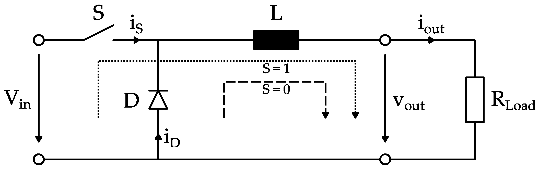
Buck converters, also known as step-down converters, are periodically switched converters, that are used to adapt a DC voltage source to a load with lower voltage ratings. The general setup is depicted in Figure 1 and consists of an arbitrary DC voltage source (Vin), a switching device (S), a freewheeling diode (D) as well as inductive (L) and ohmic (R) loads. In various applications, dedicated capacitive elements in parallel to the load are used in order to smoothen the output voltage (vout). By periodically switching S, the load is connected or disconnected from the source. This results in a current commutation process from the main current path (Vin-S-L-Load) into the freewheeling diode (D-L-Load) current path. By adequate selection of the control structure, either the mean output voltage (vout) or the output current (iout) waveform can be adjusted [30,31,32,33].
At the initial closing of the switching device, a current flow is initiated that can be calculated using Equation (1). When the switch is opened, the current commutates into the freewheeling diode path. The resulting subsiding current flow through the load is given by Equation (2). The subsequent current rise after a repeated switch-on of the switching device can be determined from Equation (3) [32].
For the considered application case of a demonstrator high-power test circuit, an insulated gate bipolar transistor (IGBT) was chosen as the power electronic (PE) switching device. The underlying reasons were enhanced controllability and high switching frequency, which are necessary for the desired functionality [35]. A mechanical switching device would not suffice.
2.2. Insulated Gate Bipolar Transistor (IGBT)
IGBTs combine the advantages of bipolar transistors (high power density) and the flexible controllability of metal oxide semiconductor field-effect transistors (MOSFET) [30,35,36]. In addition to the dedicated continuous switching modes (conducting and blocking) of IGBTs, an understanding of the dynamic switching behavior is necessary to comprehend the associated challenges in the presented practical application. For the visualization, a cross-sectional schematic of an IGBT is shown in Figure 2. In addition to the resulting MOSFET (npn) and bipolar transistor (pnp) structures at the junctions between the differently-doped regions, stray capacitances (CGE, CGC, CCE) are highlighted. These stray capacitances play crucial roles in the dynamic switching behavior of IGBTs.
For the control of the IGBT, typically gate drive units (GDU) were applied [38]. The IGBT’s switching state is changed from blocking to conductive by applying a positive supply voltage between the gate and emitter electrode. As a result, an n-conductive path is formed inside the p-doped area near the gate contact. Majority carriers, electrons, are consequently transported towards the collector electrode, which in turn reduces the area of the space charge zone. This leads to the induction of minority carriers, positively charged holes, in the n−-zone. This flooding of the n−-drift area further reduces the space charge zone, leading to a highly conductive path between collector and emitter-contact. As a supplementary result, the voltage drop between collector and emitter (VCE) also drops [32,35,36,37,39].
The relevant voltage and current waveforms during the dynamic switching operation of IGBTs in a PEBC are shown in Figure 3. These include the gate-emitter voltage VGE (upper part of Figure 3), the collector-emitter voltage VCE (continuous line in lower part of Figure 3) and the collector current IC (dashed line in lower part of Figure 3). After the active gate turn-on at t0, the input capacitance CGE is charged. Only after reaching a threshold voltage VGE(th.) at t1, the collector current IC begins to rise. During this time, the freewheeling diode is still conductive, practically holding VCE stable. Between t2 and t4, the diode is turned off and the current fully commutates towards the IGBT. During this, the Miller capacitance CGC is charged, resulting in the characteristic Miller plateau, where VGE is constant at VGE(pl.). With CGC being fully charged at t4, the IGBT is fully switched on and CGE is charged to the steady state value of VGE(on). Correspondingly, VCE drops to VCE,sat. For switch-off, the process runs in reverse, indicated in Figure 3 from t6 onwards [32,35,36,37,39].
3. Experimental Setup
The aforementioned PEBC structure’s modularization is at the core of the high-power test circuit development. Consequently, a detailed description of the modularization is given in order to convey the understanding of the practical realization and associated challenges. The most critical challenges revolve around the interconnection of the individual PEBC modules to create an overall integrated high-power test circuit. The detailed analysis of these challenges, as well as the solution approach, are presented in the following.
3.1. Power-Electronic Buck Converter Module
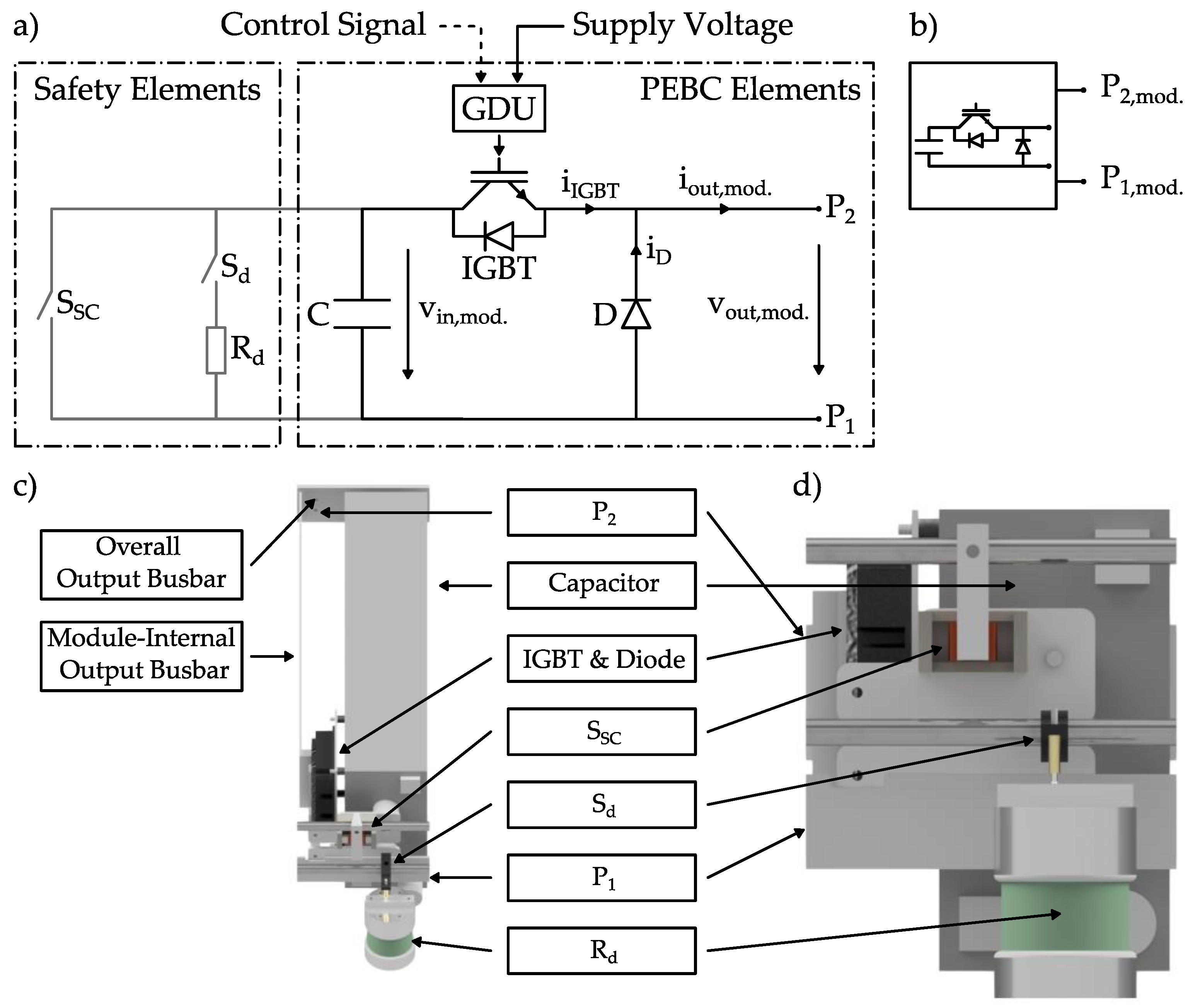
The basis for the development of individual PEBC modules is the PEBC structure, as shown in Figure 1 and explained in Section 2.1. The final design of the developed individual PEBC module is depicted in Figure 4a and explained hereafter. For purposes of illustration, a rendering of a physical PEBC module from the developed demonstrator high-power test circuit, highlighting the most important elements, is also given in Figure 4c in isometric and in Figure 4d in front view.
For the practical realization, the first decision variable is the voltage source (Vin). Since numerous individual PEBC modules are included in the final overall test circuit design, DC/DC converters, or comparable voltage sources on the module level which are directly connected to a point of common coupling, are not feasible. This is due to wiring efforts and complex galvanic isolation. To cope with these challenges, a module capacitance (C) was chosen as a dedicated energy storage unit. With this as the voltage source, the high-power test circuit can be designed as a synthetic testing environment, without direct connection to a point of common coupling during a high-power test. That means that no repercussions on the connected grid infrastructure occur. Additionally, high-power capacitances are typically comparably robust components. In combination with a relatively simple adjustment of the level of input voltage and the design as a synthetic test circuit, a flexible test circuit operation can be ensured. The choice of the specific capacitance values depends on the desired test circuit operation in terms of capacitance, maximum charge voltage and maximum discharge current. Regardless of the specific desired test circuit ratings, the general requirements for the capacitor are comparatively low: On the one hand the discharge operation is desired to be as robust as possible with current amplitudes at least as high as the switching device limits, and simultaneously a high energy density is necessary to keep the source voltage as stable as possible. In addition, the tolerance of the individual module capacitance values should be minimal in order to ensure a module voltage that is as homogeneous as possible over the entire test sequence. This was implemented in the demonstrator test circuit to the effect that discharge-capacitances with oil-impregnated self-healing metallized dielectrics were used (cf. Appendix A).
Supplementing the module capacitance, the other elements that were included on the module level and that were responsible for the PEBC functionality were a PE switching device (IGBT) and a freewheeling diode (D). The implementation of a dedicated inductance at module level was waived for reasons explained later on (cf. Section 4). The interconnection of several PEBC modules was achieved via the interconnection terminals P1 and P2. The specific interconnection coordination of several PEBC modules is explained in Section 3.2. IGBT internal anti-parallel diodes were also included, whose function was to protect the IGBT from reverse overvoltages. In the developed demonstrator high-power test circuit, the diodes were also used as a current path to charge the module capacitors prior to the actual impulse current generation for conducting experimental investigations. The corresponding procedure is described in Section 3.2.
Also included in Figure 4 are the relevant voltage measurement signals on the PEBC module level, consisting of charging voltage of the capacitance (Vin,mod.) and the module’s output voltage (Vout,mod.). The considered currents include the current through the IGBT path (iIGBT), through the diode path (iD) and the overall module output current (iout,mod.).
The active IGBT control was handled by a GDU on the module level. The inputs for the GDU are marked in Figure 4 and include the control signal and the supply voltage. The control signal was centrally computed by a central control unit (CCU) and transmitted as a synchronized signal to the GDUs on the module level. As such, the overall test circuit, consisting of several interconnected PEBC modules, virtually operated as a singular PEBC. As a consequence, the output current of the overall test circuit was chosen as the control variable instead of the individual module’s output current. Calculation and generation of the control signal was based on a two-point control scheme. The actual implementation of the regulation is not intended to be the focus of this paper. For a detailed explanation and analysis of control algorithm, reference is made to [24]. The distribution of the control signal to the individual PEBC modules is described in Section 3.3.3 of this article.
To ensure a safe operation of the high-power test circuit, the individual PEBC modules had to be extended. As direct connections to the high-voltage electrodes of the module capacitors are not provided at the overall test circuit level, possibilities for safe discharging and earthing must be provided at module level. For this, a switch (Sd) to discharge the capacitor via a discharge resistor (Rd) after a test is conducted was included. This is part of the normal operation sequence of the high-power test circuit. Additionally, a switch (SSC) to short-circuit the capacitance was added to the PEBC module design. This was an additional level of security in the normal operation mode, to make sure that no stray charges remained, even after discharging the capacitance using Sd. In case of emergency, this switch (SSC) served as an emergency grounding switch. For the operational functionality of the PEBC to generate the stresses on MVDC CB, relevant during a short-circuit interruption test, these safety measures played no role. In the subsequent graphic representations, the elements Sd, Rd and SSC are therefore neglected. For the further description, the abstract representation of an individual PEBC module, as shown in Figure 4b, is used.
3.2. Interconnection Coordination of PEBC Modules
The described design of the PEBC module containing two connection terminals, P1 and P2, allows for a flexible interconnection of several individual modules. The two interconnection options are depicted in Figure 5. Therein, Figure 5a shows the interconnection of two PEBC modules in serial connection. It is clear, that by connecting any number of PEBC modules in serial, the total output current iout,ser. cannot be enhanced, since the main current path runs through all stages of the stack. The total output voltage vout,ser., however, multiplies with the number of stages. In contrast, the parallel interconnection, as presented in Figure 5b, leads to a respective increase in the total output current iout,par.. The output voltage vout,par. remains constant. In both interconnection options, the value of the total capacity changes according to the general capacity equation.
When designing an overall integrated high-power test circuit for the investigation of DC circuit breakers on the basis of the presented modularized PEBC modules, the number of necessary modules depends on the desired application case. For the dimensioning of the test circuit, typically three design parameters are relevant [16]:
- Target current amplitude
- Level of test voltage
- Magnitude of test energy
For the provision of the aspired test current amplitude (itest,target), the corresponding number of PEBC modules were connected in parallel. The required number (m) can be calculated using Equation (4). Similarly, the required number of serial stages (n) can be calculated by Equation (5) in dependence of the target test voltage (vtest,target). For both values, it is necessary to round up to the next real number. The provision of a sufficient test energy is a combination of both, the total circuit capacitance Ctotal and the control inductance of the test circuit LControl. The total circuit capacitance is a function of the number of serial stages and parallel modules per stage and can be calculated using Equation (6).
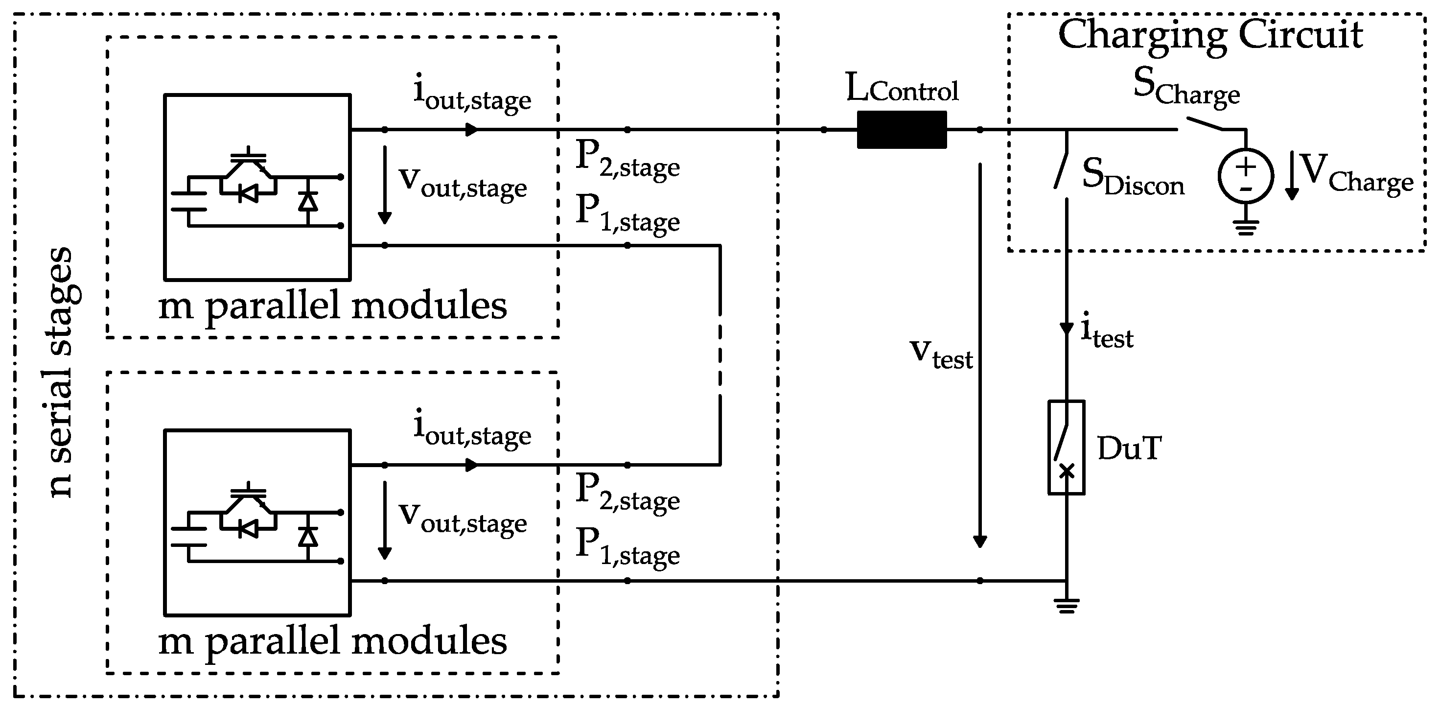
Figure 6 shows the equivalent circuit diagram of the final overall test circuit design. The aforementioned parallel and serial inclusion of individual PEBC modules can be seen on the left-hand side of the circuit diagram. It is important to note that the choice of the number of parallel modules (m) per stage is to be equalized across all stages. Besides the PEBC modules in parallel and serial connection, the only other added elements required for the general PEBC part of the test circuit are the control inductance (LControl) in the main output current path and the device under test (DuT). Similar to the choice of the module capacitance and the number of interconnected modules, the choice of LControl depends on the desired test sequences to be conducted. In this regard, the control inductance serves two purposes: On the one hand, it is used to smoothen the course of the output current and to thus support a stable test circuit operation. On the other hand, it represents the system inductance of MVDC grids. Since the energy magnetically stored in the system inductance needs to be dissipated by the DC circuit breaker during current interruption, replicating the system inductance is necessary to achieve realistic operating conditions. As additional general requirements, it can be noted that LControl needs to withstand the voltage and current stresses during a breaking test of a MVDC circuit breaker. In the demonstrator high-power test circuit, a line trap air coil with rated nominal voltages of Vr = 150 kV and a rated short-circuit current capability of Ir = 31.5 kA is applied for the aforementioned reasons. The inductance ratings can be adjusted in discrete steps as LControl = 0, 0.5 and 1.0 mH.
Supplementing the general PEBC part of the test circuit, the charging circuit is highlighted in Figure 6, which is used to charge the PEBC module capacitors pre-test through the anti-parallel IGBT-internal diodes (cf. Figure 4). Before initiating the active test current flow, the disconnector switch SDiscon is open and the switch SCharge is closed. After the PEBC module capacitances have reached the specified charging voltage, the voltage source (VCharge) is disconnected. By closing the switch SDiscon, the test circuit is closed and ready to generate the desired impulse test current.
Theoretically, the structure shown in Figure 6 allows for the design of high-power test circuits based on modularized PEBC cells in an arbitrary (m × n)-matrix. The practical realization, however, poses challenges regarding the harmonization between the individual PEBC modules. These practical challenges are discussed within the framework of this article.
3.3. Setup of Demonstrator High-Power Test Circuit
In order to prove the functionality of the developed test circuit for MVDC CB, a demonstrator high-power test circuit was built at RWTH Aachen University. The underlying requirements regarding the target current amplitude (itest) and test voltage (vtest) for the specific considered application can be obtained from Table 1. To account for a variety of different scenarios, the demonstrator high-power test circuit was designed to reach maximum current amplitudes of Îtest = 30 kA. Accompanying this, the maximum test voltage was set to Vtest,max = 8 kV. An overview of the ratings of the final PEBC module design, as well as of the overall demonstrator high-power test circuit, is included in Appendix A.
3.3.1. Realization of Integrated Overall Demonstrator Test Circuit Interconnection
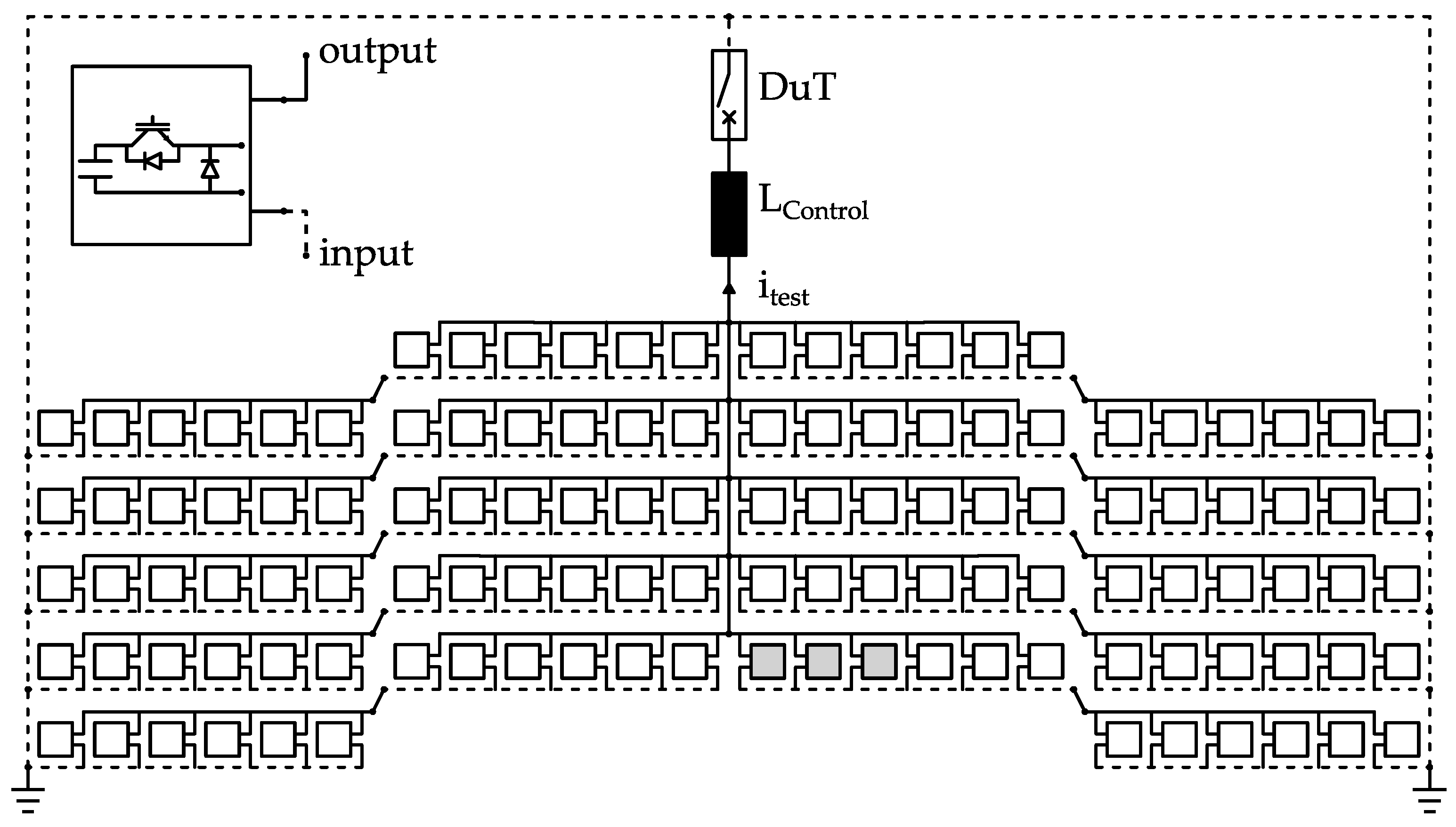
When designing electric circuits on the basis of PE equipment, it is well established that shortest possible paths between components as well as uniform distances are mandatory. For this reason, and for reasons of spatial circumstances at the location of construction, the layout of the realized test circuit was designed according to the depiction in Figure 7.
As indicated in Table 1, the resulting (m × n) matrix was chosen as a (60 × 2) matrix [24]. The individual PEBC modules were stacked in a total of four capacitor banks, containing 30 modules each. Two of each of these capacitor banks form one test circuit stage. Within the two stages, 60 modules are connected in parallel by direct connection of the respective ground terminals (P1) using common ground busbars, indicated by the dashed connecting lines in Figure 7. Similarly, the output terminals (P2) are connected by a common output busbar system (continuous lines in Figure 7). In order to provide a symmetrical interconnection between modules, the two outer capacitor banks form the first test circuit stage. The first stage’s output is routed to the ground terminals of the two inner banks, which form the second test circuit stage. The output of the second stage in turn is applied as the test current itest onto the DuT via the control inductance LControl. By designing the control inductance to be adapted in discrete steps (cf. Table A2), a variation of the rate of rise of the test current (ditest/dt) can be achieved. To visualize the spatial boundary conditions, a photo of the demonstrator high-power test circuit is given in Figure 8.
3.3.2. PEBC Modules in Master–Slave Configuration
Since the high-power test circuit is to be operated as a singular PEBC (cf. Section 3.1), potentials for reducing construction and control efforts can be exploited. For this, three PEBC modules each were combined to form a PEBC module package, as can be seen in Figure 9. The middle module is defined as the master, the two outer modules as slaves. Through this, only one centrally computed control signal and one power supply need to be connected to three modules each. The central control signal is translated by the master GDU and transmitted as the local control signal together with the supply voltage to the GDUs of the slave modules. This reduces the expenditures necessary for the amount of centrally computed control signals as well as the efforts to wire the individual PEBC modules to one third as compared to the direct connection of every individual PEBC module.
3.3.3. Overall Test Current Control System
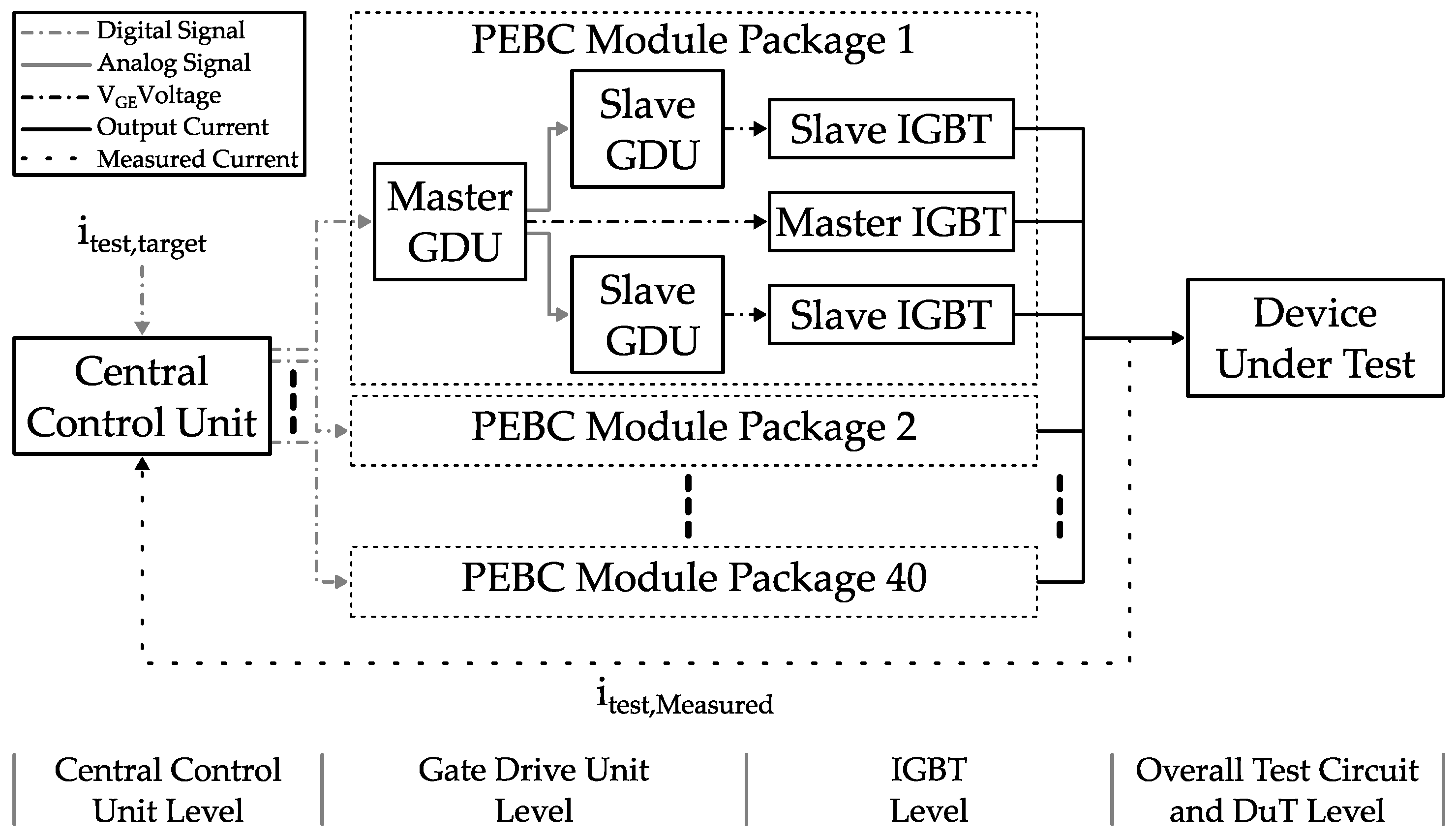
The test current (itest) applied on the DuT was chosen as the central control variable in the developed high-power test circuit. In the following, the underlying control system is described in more detail and, in particular, the distribution of the control signals to the individual PEBC modules. This is done using the schematic representation in Figure 10. As a pre-set, the target current waveform (itest,target) for the test sequence is fed into the CCU. By comparing itest,target and the measured test current, which was actually applied on the device under test (itest,Measured), the necessary state of the IGBTs is centrally computed by the CCU and translated to a switching signal. In the demonstrator test circuit, the cycle frequency of the control system is f = 100 MHz, whereas the maximum switching frequency of the applied IGBTs is limited to fmax = 10 kHz. As previously indicated, the actual implementation of the control structure, a two-point control, is not discussed in detail here. It is, however, necessary to understand that for the underlying control algorithm, a target current waveform is specified before conducting a high-power test. This target current waveform is enveloped by a tolerance band, which governs the switching limits for the CCU. If the actual test current is outside of this tolerance envelope band, the IGBTs’ switching state is changed accordingly between blocking and conducting mode. A detailed presentation and discussion of the implemented control algorithm of the developed demonstrator high-power test circuit is given in [24].
The central switching signal is computed for all 40 PEBC module packages of the overall high-power test circuit uniformly and is distributed via fiber optics to the packages’ master GDUs. In Figure 10, this is marked by the dotted grey line. The incoming switching signal is converted into an analog signal (continuous grey line) and forwarded to the slave GDUs as well as transformed into a VGE voltage for the master IGBT (finely dotted black line). The application of the VGE voltage on the master IGBT is delayed to match the internal computing time of the slave GDUs in order to achieve a simultaneous switching signal to the modules’ IGBTs. As a consequence of the rise in VGE voltage, the modules’ IGBTs become conductive and the output current flow of the modules is initiated (continuous black line) and applied on the DuT. The overall output current in turn is continuously measured and the corresponding measurement signal is fed into the CCU to compute the necessary switching state of the IGBTs for the next time step.
3.4. Investigation Scheme
As stated above, significant cost-saving potentials can be exploited through the combination of three PEBC modules into one PEBC module package in a master–slave configuration. A number of these are then interconnected as the integrated overall high-power test circuit. However, this comes at the cost of higher requirements regarding synchronization and harmonization efforts within the PEBC module package itself, as well as between numerous PEBC module packages. The associated challenges experienced by the authors during the construction and commissioning of the demonstrator high-power test circuit as well as the respective solution approaches are discussed in detail hereafter.
3.4.1. Investigated Design Options for Interconnection Coordination of PEBC Modules
The main challenges observed are related to the interconnection of the individual PEBC modules to the common output busbar of the test circuit. These impact the control stability of the demonstrator test circuit with a strong dependency on stray inductances. To demonstrate this, Figure 11 shows a schematic drawing of the integration of individual PEBC modules in the real demonstrator test circuit. As can be seen, three PEBC modules each are connected to form the PEBC module package. The input terminals of the individual PEBC modules are directly connected by a common ground busbar. The ground connection to the next PEBC module package is realized by the point of common coupling (PCC1). Preliminary investigations show that the common ground busbar has no effect on the control stability and is therefore neglected in the following. For the output connection, an output busbar is used with a connection to the next PEBC module package at PCC2. The connection to the next module package is indicated in Figure 11 by means of representation of the neighboring package (greyed-out). For the connection between the emitter terminals of the individual PEBC modules (E) and the output busbar, module-internal busbars have to be used as a result of spatial constraints in the demonstrator test circuit (cf. Figure 4). These busbars on the module level feature a busbar inductance, marked in Figure 11 as LE1–LE3. Additionally, the busbar inductances of the common output busbar sections from the individual contacting point to PCC2, LB1–LB3, are included in the graphic representation. Gate contact (G) and collector terminal (C) of the IGBTs are also highlighted in the schematic drawing.
Several options are available to interconnect these module-internal busbars to the common output busbar. In total, four different interconnection strategies, as shown in Figure 12a–d, are considered and analyzed within the framework of this article. The constructive framework conditions are identical for all four considered designs of interconnection coordination. These include the size of the common busbars, the module-internal busbar inductances LE1–LE3 as well as the positioning of the individual PEBC modules.
The first interconnection strategy, depicted in Figure 12a, represents the base case and is characterized by a connection of the PEBC modules to different connecting points on the output busbar. In Figure 12b, a redesign is realized by connection of all three PEBC modules of one PEBC module package to the same connecting point on the output busbar. The respective change is highlighted by greying out the unchanged elements. For the option depicted in Figure 12c, the design from the previous case is extended by a direct connection of the IGBT emitter terminals as a supplement to the module-internal busbars. The goal of this design is to equalize the emitter potential of the three PEBC modules. Figure 12d shows the final connection coordination design. This is the further development of the previously described designs with the implementation of an additional direct connection of the collector terminals of the IGBTs. Through this design, the voltage levels of the PEBC modules’ capacitors is achieved, further improving the control stability. In the remainder of the article, the individual options are referred to as base case a and otherwise as interconnection design options b–d. For reasons of simplicity, a repeated reference to Figure 12 will be omitted.
3.4.2. Experimental Method and Investigation Approach
For the conducted experiments regarding the impact of the interconnection design on the test circuit stability, only the initial turn-on operation is considered. This is permissible, since this switching operation constitutes the highest sensitivity to unstable test circuit operations. Thus, the actual waveform of the test current is neglected for the presented results in Section 4.1. In order to demonstrate the functionality and investigate the control stability, the experimental investigations were conducted in full operating capacity of the demonstrator test circuit. Consequently, the specified testing parameters for the experimental investigations concerning the developmental steps for the interconnection design presented in this article are listed in Table 2.
The choice of the interconnection coordination proved to have the largest impact on the control stability of the demonstrator high-power test circuit. This impact directly translates to a change in the gate-emitter voltage VGE, measurable at the GDU of the individual PEBC module. In order to monitor this behavior, the VGE-measurement of an exemplary PEBC module package was conducted. For this, active differential probes (TT-SI 9001 by TESTEC) were applied, which were measured using a central measurement system at fMeas = 100 MSamples/s. The corresponding monitored PEBC module package is indicated in Figure 7 as greyed-in.
The effects of the different interconnection designs a–d are first demonstrated by means of a comparative analysis. For this, the gate-emitter voltages VGE of the individual PEBC modules of one PEBC module package were analyzed for the time range of the initial turn-on operation, which is between t = 0 µs and t = 100 µs. Concluding, by comparison of the normalized deviation (VGE,Diff) of the slave GDU’s VGE from the VGE value of the master GDU, the control stability can be quantified. Through this analysis, the increasing control stability as a function of the further developments b–d can be demonstrated. Preliminary investigations, the presentation of which is omitted here, have shown that the uniformity of the VGE voltages directly translates to a uniformity of the PEBC module output currents.
The presentation of the results in the figures of Section 4.1. is according to the order of the interconnection options in Figure 12. Equivalently, the underlying enumeration of the results shown in the figures are chosen in accordance with the one in Figure 9, with Slave 1 being the slave module to the left and Slave 2 the one to the right of the Master module respectively.
Concluding this section, an exemplary rectangular test current generation is presented and analyzed in Section 4.2, on the basis of which the feasibility of the presented method to interconnect several high-power PEBC modules is demonstrated, thus proving the overall functionality and stability of the overall high-power test circuit.
4. Results and Discussion
4.1. Experimental Investigation of Interconnection Coordination
Since the interconnection coordination in Figure 12a represents the smallest wiring effort, this option was chosen as the base case for the demonstrator test circuit. However, during the commissioning tests on the basis of the base case design, automatic terminations by the test circuit control can be reproducibly observed, even at the lower end of the high-power test circuit’s limit spectrum. The causal chain that leads to these terminations can be found in the design of combining three individual PEBC modules each into PEBC module packages. A central control signal is generated for each PEBC module package, which is transmitted to the GDU of the master module. The master’s GDU processes the signal internally and relays it to the slave modules’ GDUs, which change the switching state of the IGBTs synchronously with the master module (cf. Section 3.3.3). At the same time, the respective gate-emitter voltage VGE of the individual modules is monitored locally at the GDU and continuously compared with the gate-emitter voltages VGE of the other two PEBC modules involved. If the deviation leaves a predefined tolerance band, this is transmitted to the CCU as an error condition, whereupon the CCU sends a switch-off signal to all GDUs of the overall test circuit and the control is aborted. To investigate this, the comparative analysis of the VGE voltages is conducted.
The first essential object of investigation is the formation of the Miller plateau, as described in Section 2.2, during the turn-on of the modules’ IGBT. Figure 13a shows the corresponding time range of the VGE voltages (VGE,Master, VGE,Slave1, VGE,Slave2) during the initial switch-on at the set parameters from Table 2 for the base case interconnection between the PEBC modules. As can be seen, the formation of the Miller plateau, between t = 4 µs and t = 7 µs, does not exhibit significant deviations between the three associated VGE voltages. However, first indications as to the subsequently growing discrepancies can be observed after t = 13 µs.
Figure 14a acts as the continuation of the identical switch-on operation as shown in Figure 13a for the time range of t = 20 µs to t = 100 µs. The target gate-emitter voltage for the applied IGBTs is VGE,target = 15 V. As is evident from the measurements, the deviations between the three measured gate-emitter voltages (VGE,Master, VGE,Slave1, VGE,Slave2) as well as from the target voltage (VGE,target) reach values of up to VGE,Diff = 2.43 V. These in turn lead to the automatic termination by the test circuit control.
The cause for the considerable deviations between VGE,Master, VGE,Slave1 and VGE,Slave2 respectively is best described using the involved inductances, highlighted in Figure 11. The GDUs are using the potential of the emitter-terminal (E) on the module level as the reference potential for setting the gate-emitter voltage VGE. Additionally, this emitter potential is taken as the reference point for the comparison between the VGE voltages within the master–slave configuration. However, since the stray inductances between the modules and the joint point of common coupling PCC2 differ in value (cf. Equations (7)–(9)), different voltage drops for all three involved PEBC modules result. This leads to different values of the emitter-potential, which the associated GDUs try to even out. Since the computing time of each GDU is finite, these matching processes interfere with each other, which ultimately leads to increasing deviations and an automatic termination by the test circuit control.
The choice of the presented parameters for the experimental investigations (itest, vtest, cf. Table 2) arises from the fact that with the base case coordination design, a stable operation above these parameters cannot be achieved. As a consequence, the coordination design of the base case is dismissed as not feasible for the provision of a stable test circuit control. The main objective of the development of new interconnection options is therefore to harmonize the emitter inductances from the terminals of the PEBC modules to the point of common coupling of the superordinate PEBC module package (LSlave1→PCC2, LMaster→PCC2, LSlave1→PCC2). The design steps are highlighted in Figure 12b–d and the results of the associated experimental investigations are discussed hereafter.
As a first step towards homogenizing the emitter inductances within the PEBC module packages, the connection of the PEBC module internal busbars to the common busbar is modified towards a common star point connection via short cables with high-current carrying capability. The added cable inductances are LE1′, LE2′ and LE3′ (LEj’), resulting in the overall inductances from each PEBC module’s emitter terminal to the PCC2, as described in Equation (10).
Considering the formation of the Miller plateau (cf. Figure 13b), no significant difference can be observed as compared to Figure 13a. This is, however, due to the fact, that the formation of the Miller plateau is not the critical phase during a switch-on operation. Nevertheless, it can be shown that the introduction of the star point connection also does not negatively impact this phase. Thus, the principle feasibility of the developed interconnection can be accepted for the formation of the Miller plateau. As a supplementary, it is evident from Figure 14b, that the redesign towards option (b) significantly improves the stability and the homogeneity of the gate-emitter voltages VGE. It is important to note, that for the base case, the ordinate-scale ranges from VGE = 11 V to VGE = 17 V, whereas in the other displayed measurement results (Figure 14b–d), the voltage scale only includes VGE = 14.5 V to VGE = 15.5 V. A presentation with a uniform scale was not feasible, as otherwise the effects studied could not be presented sufficiently well.
However, especially in the time range until VGE reaches the steady state value of VGE,on, deviations between the gate-emitter voltages of the investigated PEBC modules remain for the interconnection option (b). This can be attributed to the fact that constructive tolerances in the module internal busbars, as well as the star point connection cables, cannot be ruled out across the board. In order to reduce these differences to a minimum, direct connections between the emitter terminals are introduced in concept (c). Through this modification, the emitter potential is almost perfectly equalized within the PEBC module package. Again, the effects of the extended design in the first 20 µs of the turn-on operation (cf. Figure 13c) are negligible. For the continued switch-on operation (t = 20 µs to t = 100 µs, cf. Figure 14c), on the other hand, the impact on the homogeneity of the gate-emitter voltages (VGE) can be clearly observed. At this state of the design, the space for optimization regarding the harmonization of the emitter inductances is exhausted in constructional terms. However, minor deviations still persist between the considered VGE voltages.
The last parameter with potential for optimization within the confines of the constructive and peripherical boundary conditions of the demonstrator test circuit is the harmonization of the charging voltages of the module capacitors. These impact the VGE voltages, since a higher charging voltage of one module capacitor leads to a higher module output current and thus to a higher voltage drop across the busbar to the star point connection. Since PE equipment is sensitive to even small deviations, already capacitance variances of the module capacitors due to manufacturing tolerances can lead to instabilities. This challenge is resolved by the introduction of direct connections between the high voltage terminals of the module capacitors within a PEBC module package. Through this constructive extension, the level of the charging voltage can be homogenized for all three PEBC modules. The resulting VGE measurements (Figure 13d and Figure 14d) prove the effectivity of the developed design for the interconnection coordination within one PEBC module package. In order to avoid propagation of the fault in the event of a failure, the high-voltage electrodes of all test circuit modules are not connected directly to each other in the practical implementation. Although this would in theory lead to a homogenized source voltage distribution across the entire test circuit, it might also lead to an uncontrolled discharge of all involved modules into one faulty module and consequently in the worst case to the destruction of the module. The uniform charging level of the test circuit is realized through the charging circuit, as depicted in Figure 6, which is used to supply the entire test circuit charge from one source. As the results presented in Section 4.2 demonstrate, the measure to directly connect all high-voltage electrodes of one test circuit stage is not necessary for a stable and secure operation of the developed demonstrator high-power test circuit. It is, however, recognized that this design parameter can serve as an optimization potential in future applications.
As a quantitative measure to assess the effectiveness of the interconnection developments, the absolute value of the deviation (VGE,Diff) between the master’s VGE and the slaves’ VGE, is determined. The results are shown in Figure 15a–d. Already an optical inspection of the results reveals the gradual effects, starting from the base case (a) to the subsequent further development steps b–d.
A gradual reduction of the absolute value for VGE,Diff can be observed as the complexity of the interconnection coordination increases and approaches the optimum (from a to d). The respective values are included in Table 3. Through the presented optimized interconnection design d), a reduction of VGE,Diff by 90.5%, as compared to the base case a, can be achieved. This improves the test circuit control stability significantly and ensures the integrated functionality of interconnected high-power PEBC modules. For (a) reliable test circuit control, this value needs to be limited to a maximum deviation of VGE,Diff < 1.0 V.
The results presented above support the decision not to integrate control inductances at the PEBC module level. Even small deviations in the stray inductances, which are typically orders of magnitude smaller than dedicated control inductances, lead to increasing difficulties regarding the control stability of the high-power test circuit. Since production-specific tolerances of the actual inductance ratings cannot be ruled out, this uncertainty factor is eliminated from the outset in the development process of the modular high-power test circuit.
4.2. Experimental Demonstration of Presented Interconnection Method
In order to demonstrate the feasibility of the described method of interconnecting multiple high-power PEBC modules to form one overall high-power test circuit, an exemplary test current generation is analyzed. For this purpose, a rectangular test current waveform with an amplitude of îtest,target = 10.0 kA for a duration of t = 50 ms is specified as the target current (cf. Table 4). The test circuit capacitances are pre-charged to Vtest,overall = 3.0 kV, which translates to the individual modules being charged to Vtest,module = 1.5 kV. For the presented experimental demonstration, the control inductance is set to LControl = 0.5 mH. The underlying control algorithm applied is a two-point control, which is described in detail in [24].
The specified target current waveform (itest,target, dashed grey), the generated test current (itest, continuous black) and the corresponding course of the overall test circuit voltage (vtest, continuous grey) for the conducted experiment are depicted in Figure 16.
At t = 0 ms, the CCU distributes a switching signal, HIGH, to the PEBC modules of the test circuit, which is realized according to the control flow chart in Figure 10. This initiates the current flow. Simultaneously, the test circuit voltage decreases as a result of the capacitors being discharged to feed the test current. At t = 1.7 ms, the upper target current envelope limit is reached and the CCU changes the switching signal to LOW. As a result, the current flow commutates to the free-wheeling diodes of the PEBC modules and the overall test current decreases due to ohmic losses and the losses in the DuT. At t = 1.96 ms, the lower target current limit is reached and the CCU changes the control signal back to HIGH, leading to a renewed increase in test current due to a further discharge of the capacitors. In this time range, the test circuit voltage decreases equivalently. This process is repeated until the end of the pre-set target current is reached (t = 50 ms) and the CCU transmits a continuous LOW signal to end the control sequence and to switch off the IGBTs.
Two phenomena need to be addressed with regards to the adequacy of the target current mapping: the finite rate of rise, respectively, the rate of fall of the generated test current and its ripple. As a result of the slope-limiting characteristics of the combined circuit inductances, the actually generated test current does not match the rate of rise of the pre-set target current. However, this is not a restriction for the intended test operation, as the field of application of the developed high-power test circuit is the simulation of realistic fault currents in future MVDC grids. The finite rate of rise adequately represents that of realistic use cases. At the end of the control sequence (t = 50 ms), the test current subsides with a relatively low rate of fall as compared to the target current curve. This is due to the magnetic energy stored in the control inductance and does also not restrict the applicability of the developed test circuit design, since this energy is to be absorbed by the MVDC circuit breaker during current interruption operation. The resulting ripple of the test current (i.e., ∆I ≤ 320 A, 3.2% of the target current amplitude in the presented test scenario) is a result of the finite switching frequency of the applied IGBTs and corresponding GDUs. In order to operate the PE switching devices in a permissible operation state, minimum on- and respectively off-times need to be adhered to. As with the previously discussed current slopes, the current ripple does not represent a functional limitation either, since it is in a comparatively low range on the one hand and, on the other hand, fault currents in future MVDC networks also exhibit current ripples.
When considering the course of the test circuit voltage over the duration of the conducted test, voltage spikes and oscillations are clearly observable during every switching operation of the IGBTs. These can be attributed to PEBC module internal commutation processes from the IGBT to the freewheeling diode, and vice versa. These processes are component-dependent and cannot be influenced through constructive measures outside of the PE switching equipment. For the test voltage, as seen by the DuT, these phenomena are negligible.
As is evident from the presented results in Figure 16, the applied and previously discussed measures to harmonize the PEBC module internal emitter inductances, as well as the respective modules’ charging levels, sufficiently stabilize the test circuit control and enable a stable and effective high-power test circuit operation. By adjusting the control algorithm to the desired test current waveform, the generation of near-arbitrary monopolar test currents is possible and the feasibility of interconnecting multiple high-power PEBC modules to form an overall high-power test circuit that can be virtually operated as one singular PEBC is thus demonstrated and supported by the presented results.
5. Conclusions
This article describes and analyzes the interconnection of individual power-electronic buck converter modules in an integrated high-power test circuit for the investigation of a MVDC circuit breaker. The modularization is necessary to achieve adequate testing ratings for the proper representation of realistic stresses on MVDC switching equipment during a short-circuit current interruption. However, this modularization necessitates the interconnection of such PEBC modules into an overall high-power test circuit, which is operated as one integrated singular PEBC. In order to reduce wiring as well as control signal generation and distribution efforts, three individual PEBC modules each were combined into one PEBC module package.
During the practical implementation of a demonstrator high-power test circuit, challenges with regard to the test circuit control stability were observed. These can be attributed to differing emitter inductances of the interconnection busbar setup. From the presented experimental results, derivations of design criteria for the interconnection of high-power PEBC modules can be made. The authors cannot stress enough the importance of harmonization efforts for the interconnection of high-power PEBC modules in an integrated high-power test circuit. In addition to the choice of a star-point connection instead of distributed connection to a common busbar system, the emitter potential of the PEBC modules should be as homogeneous as possible. This can be either realized by constructive efforts to place the IGBTs as close together as possible, or by equalizing the emitter potentials by means of low-inductance connections.
Concluding, the design of low-inductance interconnections of high-power PEBC modules significantly enhances the control stability and as a direct consequence the achievable power rating. Additionally, it is important to ensure a balanced charging voltage of the module capacitors. If one adheres to these guidelines, the interconnection of several high-power PEBC modules into one integrated high-power test circuit has been proven to be functional. With the presented modularization and interconnection options, arbitrary test circuit ratings can be achieved and are available for adaptations to future use cases. The functionality of the demonstrator high-power test circuit is proven by analysis of an exemplary test current generation of îtest = 10.0 kA at Vtest = 3.0 kV. A detailed description of the general functioning as well as the underlying control algorithm of the high-power test circuit is given in [23,24].
Author Contributions
Conceptualization, N.L. and A.M.; methodology, N.L.; validation, N.L.; formal analysis, N.L.; investigation, N.L. and S.K.; resources, A.M.; data curation, N.L.; writing—original draft preparation, N.L.; writing—review and editing, A.M., S.K.; visualization, N.L.; supervision, A.M.; project administration, N.L. All authors have read and agreed to the published version of the manuscript.
Funding
This research was funded by the German federal Ministry for Economic Affairs and Energy, grant number 03ET7548.
Data Availability Statement
Not applicable.
Conflicts of Interest
The authors declare no conflict of interest.
Appendix A

Table A1.
Ratings of individual PEBC module.
| Parameter | Symbol | Value | Unit |
|---|---|---|---|
| Maximum Module Current | ÎModule | 500 | A |
| Maximum Module Voltage | VModule,max | 4 | kV |
| Module Capacity | CModule | 2 | mF |
| Maximum Module Energy | EModule,max | 16 | kJ |
Table A2.
Ratings of overall high-power test circuit.
| Parameter | Symbol | Value | Unit |
|---|---|---|---|
| Maximum Test Circuit Current | Îtotal | 30 | kA |
| Maximum Test Circuit Voltage | Vtotal,max | 8 | kV |
| Maximum Test Circuit Capacity | Ctotal,max | 60 | mF |
| Maximum Test Circuit Energy | Etotal,max | 1.92 | MJ |
| Test Circuit Inductance | LControl | 0.5, 1.0 | mH |
| Maximum Test Current Slope | di/dtmax | 16 | kA/ms |
| Total Number of Modules | 120 |
References
- EU European Union. Renewable Energy: Fact Sheet of the European Union. 2021. Available online: https://www.europarl.europa.eu/factsheets/en/sheet/70/renewable-energy (accessed on 12 September 2022).
- IPCC (Intergovernmental Panel on Climate Change). Global Warming of 1.5°C—Summary for Policymakers; IPCC: Geneva, Switzerland, 2018. [Google Scholar]
- IRENA (International Renewable Energy Agency). Renewable Capacity Statistics 2021; IRENA: Abu Dhabi, United Arab Emirates, 2021. [Google Scholar]
- Grainger, B. Medium Voltage DC System Architectures; Energy Engineering Series; Institution of Engineering & Technology: London, UK, 2022. [Google Scholar]
- Priebe, J. Strukturelle Ausgestaltung von Mittelspannungsnetzen auf Basis von Gleichstromtechnologie unter Berücksichtigung einer Leistungsflusssteuerung. Ph.D. Thesis, RWTH Aachen University, Aachen, Germany, 2020. [Google Scholar]
- Coffey, S.; Timmers, V.; Li, R.; Wu, G.; Egea-Àlvarez, A. Review of MVDC Applications, Technologies, and Future Prospects. Energies 2021, 14, 8294. [Google Scholar] [CrossRef]
- Cigré. WG C6.31: Medium Voltage Direct Current (MVDC) Grid Feasibility Study; Technical Brochure TB793; Cigré: Paris, France, 2020. [Google Scholar]
- De Doncker, R.W. Power electronic technologies for flexible DC distribution grids. In Proceedings of the 2014 International Power Electronics Conference (IPEC-Hiroshima 2014—ECCE ASIA), Hiroshima, Japan, 18–21 May 2014; IEEE: Piscataway, NJ, USA, 2014; pp. 736–743. [Google Scholar] [CrossRef]
- Kusic, G.L.; Reed, G.F.; Svensson, J.; Wang, Z. A case for medium voltage DC for distribution circuit applications. In Proceedings of the 2011 IEEE/PES Power Systems Conference and Exposition, Phoenix, AZ, USA, 20–23 March 2011; IEEE: Piscataway, NJ, USA, 2011; pp. 1–7. [Google Scholar] [CrossRef]
- Carpita, M.; Dujic, D.; Christe, A.; Milovanovic, S.; Utvic, M.; Schultz, T.; Franck, C.M.; Razzaghi, R.; Wang, Z.; Paolone, M.; et al. Direct Current Technologies for Switzerland’ s Electricity Transmission and Distribution: White Paper on DC Technologies; Swiss Innovation Agency (Innosuisse): Bern, Switzerland, 2019. [Google Scholar]
- VDE (Verband der Elektrotechnik Elektronik Informationstechnik e.V.). Gleichspannung in der Elektrischen Energieverteilung: Grundsatzstudie; VDE: Frankfurt am Main, Germany, 2019. [Google Scholar]
- Stumpe, M.; Tünnerhoff, P.; Schnettler, A.; Schmidt, D. Grid topology and technology influences on selective protection concepts for multi-terminal medium voltage DC grids. J. Eng. 2018, 2018, 796–801. [Google Scholar] [CrossRef]
- Pei, X.; Cwikowski, O.; Vilchis-Rodriguez, D.S.; Barnes, M.; Smith, A.C.; Shuttleworth, R. A review of technologies for MVDC circuit breakers. In Proceedings of the IECON 2016—42nd Annual Conference of the IEEE Industrial Electronics Society, Florence, Italy, 24–27 October 2016; IEEE: Piscataway, NJ, USA, 2016; pp. 3799–3805. [Google Scholar] [CrossRef]
- He, J.; Chen, K.; Li, M.; Luo, Y.; Liang, C.; Xu, Y. Review of protection and fault handling for a flexible DC grid. Protect. Control Mod. Power Syst. 2020, 5, 15. [Google Scholar] [CrossRef]
- Langenberg, N.; Bendig, M.; Wienkamp, P.; Würde, A.; Moser, A. Prospective Fault Currents in MVDC Distribution Grids—An Evaluation Methodology. In Proceedings of the NEIS 2021: Conference on Sustainable Energy Supply and Energy Storage Systems, Hamburg, Germany, 13–14 September 2021; Schulz, D., Ed.; VDE Verlag: Berlin, Germany, 2021; pp. 166–171. [Google Scholar]
- Belda, N.A. HVDC Circuit Breakers—Test Requirements, Methods and Circuits. Ph.D. Thesis, TU Darmstadt, Darmstadt, Germany, 2021. [Google Scholar]
- Cigré. JWG A3/B4.34: Technical Requirements and Specifications of State-of-the-Art HVDC Switching Equipment; Technical Brochure TB683, Technical Brochure/CIGRE; CIGRE: Paris, France, 2017; Volume 683. [Google Scholar]
- Cigré. JWG B4/A3: Design, Test and Application of HVDC Circuit Breakers; Technical Brochure TB 873; CIGRE: Paris, France, 2022. [Google Scholar]
- Franck, C.M. HVDC Circuit Breakers: A Review Identifying Future Research Needs. IEEE Trans. Power Deliv. 2011, 26, 998–1007. [Google Scholar] [CrossRef] [Green Version]
- Gao, Y.; Han, Y.; Zhang, J.; Xiao, F.; Zhao, Y.; Li, L. Study on Fault Current Characteristics and Current Limiting Method of Plug-In Devices in VSC-DC Distribution System. Energies 2019, 12, 3159. [Google Scholar] [CrossRef] [Green Version]
- Li, G.; Liang, J.; Balasubramaniam, S.; Joseph, T.; Ugalde-Loo, C.E.; Jose, K.F. Frontiers of DC circuit breakers in HVDC and MVDC systems. In Proceedings of the 2017 IEEE Conference on Energy Internet and Energy System Integration (EI2), Beijing, China, 26–28 November 2017; IEEE: Piscataway, NJ, USA, 2017; pp. 1–6. [Google Scholar] [CrossRef]
- Bucher, M.K. Transient Fault Currents in HVDC VSC Networks During Pole-to-Ground Faults. Ph.D. Thesis, ETH Zurich, Zürich, Switzerland, 2014. [Google Scholar]
- Langenberg, N.; Krampert, T.; Heidemann, M. Development of a Modular High-Power Test Circuit for Components of Future Direct Current Grids. In Proceedings of the 21st International Symposium on High Voltage Engineering, Budapest, Hungary, 26–30 August 2019; Németh, B., Ed.; Lecture Notes in Electrical Engineering. Springer International Publishing: Berlin/Heidelberg, Germany, 2020; pp. 885–893. [Google Scholar] [CrossRef]
- Langenberg, N.; Kimpeler, S.; Wienkamp, P.; Würde, A.; Moser, A. Innovative Synthetic High-Power Test Circuit for the Investigation of MVDC Circuit Breakers—Setup, Functionality and Application. In Proceedings of the VDE Hochspannungstechnik 2022: VDE Fachtagung, Berlin, Germany, 8–10 November 2022. accepted, in print. [Google Scholar]
- Ali, S.; Shengxue, T.; Jianyu, Z.; Ali, A.; Nawaz, A. An Implementation of Parallel Buck Converters for Common Load Sharing in DC Microgrid. Information 2019, 10, 91. [Google Scholar] [CrossRef] [Green Version]
- Guerrero, E.; Guzmán, E.; Linares, J.; Martínez, A.; Guerrero, G. FPGA-based active disturbance rejection velocity control for a parallel DC/DC buck converter-DC motor system. IET Power Electron. 2020, 13, 356–367. [Google Scholar] [CrossRef]
- Mazumder, S.K.; Tahir, M.; Kamisetty, S.L. Wireless PWM Control of a Parallel DC–DC Buck Converter. IEEE Trans. Power Electron. 2005, 20, 1280–1286. [Google Scholar] [CrossRef]
- Tsang, C.-W.; Foster, M.; Stone, D.; Gladwin, D. Active current ripple cancellation in parallel connected buck converter modules. IET Power Electron. 2013, 6, 721–731. [Google Scholar] [CrossRef]
- Zhang, X.; Ruan, X.; Zhong, Q.-C. Improving the Stability of Cascaded DC/DC Converter Systems via Shaping the Input Impedance of the Load Converter with a Parallel or Series Virtual Impedance. IEEE Trans. Ind. Electron. 2015, 62, 7499–7512. [Google Scholar] [CrossRef]
- Erickson, R.W. DC-DC Power Converters. In Wiley Encyclopedia of Electrical and Electronics Engineering; Webster, J.G., Ed.; John Wiley & Sons, Inc.: Hoboken, NJ, USA, 2001. [Google Scholar] [CrossRef]
- Mohan, N.; Undeland, T.M.; Robbins, W.P. Power Electronics: Converters, Applications, and Design, 2nd ed.; Wiley: Hoboken, NJ, USA, 1995. [Google Scholar]
- Schröder, D.; Marquardt, R. (Eds.) Leistungselektronische Schaltungen; Springer: Berlin/Heidelberg, Germany, 2019. [Google Scholar] [CrossRef]
- Vinod, S.; Balaji, M.; Prabhakar, M. Robust control of parallel buck fed buck converter using hybrid fuzzy PI controller. In Proceedings of the 2015 IEEE 11th International Conference on Power Electronics and Drive Systems, Sydney, Australia, 9–12 June 2015; IEEE: Piscataway, NJ, USA, 2015; pp. 347–351. [Google Scholar] [CrossRef]
- Pavlovic, T.; Bjazic, T.; Ban, Z. Simplified Averaged Models of DC–DC Power Converters Suitable for Controller Design and Microgrid Simulation. IEEE Trans. Power Electron. 2013, 28, 3266–3275. [Google Scholar] [CrossRef]
- Volke, A.; Hornkamp, M. IGBT Modules: Technologies, Driver and Application, 2nd ed.; Infineon Technologies AG: Neubiberg, Germany, 2012. [Google Scholar]
- Perret, R.; Aloïsi, P.; Austin, P.; Béroual, A.; Breil, M.; Chatroux, D.; Clavel, E.; Costa, F.; Gautier, C.; Guena, A.; et al. Power Electronics Semiconductor Devices; ISTE: London, UK; Wiley: Hoboken, NJ, USA, 2009. [Google Scholar]
- Wintrich, A.; Nicolai, U.; Tursky, W.; Reimann, T. Applikationshandbuch Leistungshalbleiter; SEMIKRON International GmbH: Nürnberg, Germany, 2010. [Google Scholar]
- Drexhage, P. Gate Driver Basics: Application Note AN 21-002; Semikron: Nuremberg, Germany, 2021. [Google Scholar]
- Khanna, V.K. Insulated Gate Bipolar Transistor IGBT Theory and Design; John Wiley & Sons, Inc.: Hoboken, NJ, USA, 2003. [Google Scholar] [CrossRef]
Figure 1.
Equivalent circuit diagram of a buck converter. The two dedicated current paths are indicated by differently dashed lines [34].
Figure 1.
Equivalent circuit diagram of a buck converter. The two dedicated current paths are indicated by differently dashed lines [34].

Figure 2.
Cross-sectional drawing of an insulated gate bipolar transistor (IGBT) structure [37].
Figure 2.
Cross-sectional drawing of an insulated gate bipolar transistor (IGBT) structure [37].

Figure 3.
Idealized voltage (VGE, VCE, continuous lines) and current (IC, dashed line) switching characteristics during turn-on and turn-off operation of an IGBT [38].
Figure 3.
Idealized voltage (VGE, VCE, continuous lines) and current (IC, dashed line) switching characteristics during turn-on and turn-off operation of an IGBT [38].

Figure 4.
Equivalent circuit diagram of the developed individual PEBC module in (a) detailed and (b) simplified representation as well as rendering of physical PEBC module from demonstrator high-power test circuit in (c) isometric and (d) front view.
Figure 4.
Equivalent circuit diagram of the developed individual PEBC module in (a) detailed and (b) simplified representation as well as rendering of physical PEBC module from demonstrator high-power test circuit in (c) isometric and (d) front view.

Figure 5.
Interconnection options of individual PEBC modules in (a) serial and (b) parallel interconnection.
Figure 5.
Interconnection options of individual PEBC modules in (a) serial and (b) parallel interconnection.

Figure 6.
Schematic circuit diagram of integrated overall test circuit with test current (itest) and voltage (vtest) applied on a device under test (DuT).
Figure 6.
Schematic circuit diagram of integrated overall test circuit with test current (itest) and voltage (vtest) applied on a device under test (DuT).

Figure 7.
Schematic visualization of the interconnection of, in total, 120 individual PEBC modules in demonstrator high-power test circuit. The three PEBC modules used for the experiments’ measurements are indicated as greyed PEBC modules.
Figure 7.
Schematic visualization of the interconnection of, in total, 120 individual PEBC modules in demonstrator high-power test circuit. The three PEBC modules used for the experiments’ measurements are indicated as greyed PEBC modules.

Figure 8.
Photo of the demonstrator high-power test circuit with capacitor banks containing individual PEBC modules (left) and control inductance (right). The device under test (DuT) is placed in a spatially separate area for reasons of personnel and system safety.
Figure 8.
Photo of the demonstrator high-power test circuit with capacitor banks containing individual PEBC modules (left) and control inductance (right). The device under test (DuT) is placed in a spatially separate area for reasons of personnel and system safety.

Figure 9.
Schematic overview of the provision of central control signal (dashed) and power supply (continuous) infrastructure to a PEBC module package in master–slave configuration.
Figure 9.
Schematic overview of the provision of central control signal (dashed) and power supply (continuous) infrastructure to a PEBC module package in master–slave configuration.

Figure 10.
Schematic representation of the control structure and signal distribution of the demonstrator test circuit including digital and analog switching signals, VGE voltages, output currents and current measurement signals with one exemplary PEBC module package included in more detail.
Figure 10.
Schematic representation of the control structure and signal distribution of the demonstrator test circuit including digital and analog switching signals, VGE voltages, output currents and current measurement signals with one exemplary PEBC module package included in more detail.

Figure 11.
Schematic drawing of the circuitry of a PEBC module package with connection to the neighboring package (greyed out) at PCC1 (common ground) and PCC2 (common output).
Figure 11.
Schematic drawing of the circuitry of a PEBC module package with connection to the neighboring package (greyed out) at PCC1 (common ground) and PCC2 (common output).

Figure 12.
Setup of interconnection coordination for experimental investigations with (a) base case and (b–d) further developments. Highlighted elements are changes compared to the respective previous design.
Figure 12.
Setup of interconnection coordination for experimental investigations with (a) base case and (b–d) further developments. Highlighted elements are changes compared to the respective previous design.

Figure 13.
Experimental results of the gate-emitter voltage (VGE) of three PEBC modules of one PEBC module package with focus on the formation of the Miller plateau during switch-on operation of IGBTs for the investigated interconnection designs (a–d) as presented in Figure 12.
Figure 13.
Experimental results of the gate-emitter voltage (VGE) of three PEBC modules of one PEBC module package with focus on the formation of the Miller plateau during switch-on operation of IGBTs for the investigated interconnection designs (a–d) as presented in Figure 12.

Figure 14.
Experimental results of the gate-emitter voltage (VGE) of three PEBC modules of one PEBC module package during switch-on operation of IGBTs for the investigated interconnection designs (a–d) as presented in Figure 12. Note: Ordinate-scale in (a) differs from ordinate- scales in (b–d).
Figure 14.
Experimental results of the gate-emitter voltage (VGE) of three PEBC modules of one PEBC module package during switch-on operation of IGBTs for the investigated interconnection designs (a–d) as presented in Figure 12. Note: Ordinate-scale in (a) differs from ordinate- scales in (b–d).

Figure 15.
Experimental results of the absolute deviation of the slave PEBC modules’ from the master PEBC modules’ gate-emitter voltage VGE during switch-on operation of IGBTs for the investigated interconnection designs (a–d) as presented in Figure 12.
Figure 15.
Experimental results of the absolute deviation of the slave PEBC modules’ from the master PEBC modules’ gate-emitter voltage VGE during switch-on operation of IGBTs for the investigated interconnection designs (a–d) as presented in Figure 12.

Figure 16.
Experimental results for exemplary test current (Itest) generation (continuous black) with target current amplitude of Itest,target = 10.0 kA (dashed black) at an initial source voltage of Vtest = 3.0 kV (continuous grey).
Figure 16.
Experimental results for exemplary test current (Itest) generation (continuous black) with target current amplitude of Itest,target = 10.0 kA (dashed black) at an initial source voltage of Vtest = 3.0 kV (continuous grey).

Table 1.
Design requirements for demonstrator high-power test circuit and derivation of the correspondingly necessary number of test circuit stages and number of test circuit modules per stage.
Table 1.
Design requirements for demonstrator high-power test circuit and derivation of the correspondingly necessary number of test circuit stages and number of test circuit modules per stage.
| Parameter | Value |
|---|---|
| Level of Maximum Current Amplitude | 30 kA |
| Resulting number of parallel modules per stage 1 | 60 |
| Level of Maximum Test Voltage | 8 kV |
| Resulting number of stages 2 | 2 |
1 maximum module current is 500 A, limited by chosen IGBT (cf. Appendix A), 2 maximum module voltage is 4000 V, limited by chosen capacitor (cf. Appendix A).
Table 2.
Values of testing parameters for presented experimental investigation of interconnection designs from Figure 12a–d.
Table 2.
Values of testing parameters for presented experimental investigation of interconnection designs from Figure 12a–d.
| Parameter | Value |
|---|---|
| Test Circuit Capacitance | 60 mF |
| Test Circuit Inductance | 1 mH |
| Overall Charging Voltage | 400 V |
| Module Charging Voltage | 200 V |
| Target Current Amplitude | 500 A |
Table 3.
Maximum absolute values of deviation between the master VGE and the slaves’ VGE for the interconnection options of the base case (a) and the subsequent further developments (b–d).
Table 3.
Maximum absolute values of deviation between the master VGE and the slaves’ VGE for the interconnection options of the base case (a) and the subsequent further developments (b–d).
| Considered Interconnection Design | Maximum Absolute Deviation VGE,Diff |
|---|---|
| Base case (a) | 2.43 V |
| Development (b) | 0.87 V |
| Development (c) | 0.63 V |
| Development (d) | 0.23 V |
Table 4.
Values of testing parameters for experimental demonstration of presented interconnection method.
Table 4.
Values of testing parameters for experimental demonstration of presented interconnection method.
| Parameter | Value |
|---|---|
| Test Circuit Capacitance | 60 mF |
| Test Circuit Inductance | 0.5 mH |
| Overall Charging Voltage | 3.0 kV |
| Module Charging Voltage | 1.5 kV |
| Target Current Amplitude | 10.0 kA |
| Length of Control Sequence | 50 ms |
Publisher’s Note: MDPI stays neutral with regard to jurisdictional claims in published maps and institutional affiliations. |
© 2022 by the authors. Licensee MDPI, Basel, Switzerland. This article is an open access article distributed under the terms and conditions of the Creative Commons Attribution (CC BY) license (https://creativecommons.org/licenses/by/4.0/).
Share and Cite
MDPI and ACS Style
Langenberg, N.; Kimpeler, S.; Moser, A. Interconnecting Power-Electronic Buck Converter Modules in a Novel High-Power Test Bench for MVDC Circuit Breakers. Energies 2022, 15, 7915. https://0-doi-org.brum.beds.ac.uk/10.3390/en15217915
AMA Style
Langenberg N, Kimpeler S, Moser A. Interconnecting Power-Electronic Buck Converter Modules in a Novel High-Power Test Bench for MVDC Circuit Breakers. Energies. 2022; 15(21):7915. https://0-doi-org.brum.beds.ac.uk/10.3390/en15217915
Chicago/Turabian StyleLangenberg, Nils, Simon Kimpeler, and Albert Moser. 2022. "Interconnecting Power-Electronic Buck Converter Modules in a Novel High-Power Test Bench for MVDC Circuit Breakers" Energies 15, no. 21: 7915. https://0-doi-org.brum.beds.ac.uk/10.3390/en15217915
Note that from the first issue of 2016, this journal uses article numbers instead of page numbers. See further details here.