
Optimal Temperature Regulation of Integrated Circuits with Peltier Heat Pumps


1
Department of Electronics and Information Systems, University of Ghent, Technologiepark Zwijnaarde 126, 9052 Zwijnaarde, Belgium
2
Institute of Electronics, AGH University of Science and Technology, Al. Mickiewicza 30, 30-059 Kraków, Poland
3
Department of Marine Electronics, Gdynia Maritime University, Morska 83, 81-225 Gdynia, Poland
*
Author to whom correspondence should be addressed.
Energies 2022, 15(3), 1125; https://0-doi-org.brum.beds.ac.uk/10.3390/en15031125
Submission received: 9 January 2022
/
Revised: 27 January 2022
/
Accepted: 31 January 2022
/
Published: 3 February 2022
(This article belongs to the Special Issue Latest Advances in Electrothermal Models II)
Abstract
:A thermal network will be presented to model a multi-layer structure consisting of a semiconductor structure, integrated Peltier heat pump and a cooling fin. A criterion will be set up to determine the optimal Peltier current to minimise the chip temperature using the power dissipation as the control parameter. Compared with classical methods, the proposed solution does not show any time delays in response to power changes and is not sensitive to the position of chip temperature sensors. It does not generate chip temperature oscillations. The idea can be applied in each integrated circuit cooled with Peltier heat pumps, e.g., power devices, high-performance processors, high-frequency integrated circuits, etc. The authors present a simple mathematical formula that can be easily implemented in the software of a processor being cooled. As a consequence, the device is able to operate with maximum efficiency assuming required reliability. Theoretical considerations are illustrated by some results of computations. The paper is addressed to designers involved in the creation of devices dissipating a significant amount of heat energy.
1. Introduction
Currently, high-performance processors and devices dissipate heat of 300 Watts and more, which requires very efficient cooling systems.
In CMOS circuits, power consumption depends mostly upon clock frequency. Presently, in CMOS technology of 10 nm and less, power losses consist of two components: the first one is a DC value in a stand-by-state caused by the constant leakage current (static component), and the other is proportional to the clock frequency, which is called the dynamic component. Each time a circuit switches its logical state, all capacitances are charged or discharged, giving rise to a fixed amount of energy to be converted into heat. The higher the clock frequency, the more switching per time unit and the more heat is generated. For the CMOS technology up to 1 µm (e.g., high voltage devices) [1], the leakage current is relatively small, so mostly dynamic heat generation has to be considered. The power consumption is then just proportional to the clock frequency [2]. Digital integrated circuits are normally operating at a fixed clock frequency. This basic clock signal being generated by an external quartz crystal oscillator guarantees a very stable frequency. Sometimes the clock frequency fed to a circuit is reduced intentionally or automatically to reduce power consumption. Nevertheless, as long as we use data processing by means of electron devices, we have to consider energy losses.
Due to the high power dissipations in present-day electronics, cooling and temperature management are and will be an important topic [2,3,4,5,6,7,8,9,10,11,12,13]. Although fan cooling is the most widely used, other alternatives such as natural convection, liquid cooling, heat pipes, new materials, Peltier heat pumps, harvesting, etc. are also used. Their selection and application depend on the kind of heat source to be cooled, availability of stationary energy sources, accepted size limit, weight, noise level, etc. [14,15,16,17,18,19,20,21,22,23,24,25,26,27].
Fan cooling is quite efficient, but a fan produces noise and suffers from limited mechanical reliability. In this paper, we present a short theoretical study on Peltier cooling of integrated circuits. A Peltier cell pumps the heat from the front side (cold junction) to the back one (hot junction). The hot side has still to be cooled convectively. Nevertheless, the main job of the Peltier cell is to actively transfer the heat from a small area of the integrated circuit to a larger area so that even natural convection will then be sufficient for cooling the hot side of the Peltier cell. Otherwise, if one still wants to use forced convection cooling, one of the major advantages (i.e., no moving parts) is becoming lost [17].
The paper contains the answer to the question of how to control the Peltier heat pump to achieve the required influence on the temperature of a cooled semiconductor chip. The problem seems to be crucial, especially from two points of view: how to achieve a minimum chip temperature and to obtain maximum device throughput. The throughput improvement in the thermal aspect has been criticised by many authors [3,4,7,9,15,26].
A shrinking CMOS channel up to 7 nm and less (if possible) is very close to the limit of reachability from a physical point of view [28,29,30]. The main challenge for these high-performance devices is to ensure proper working temperature to reduce the interior energy density of the semiconductor structure. Decreasing the semiconductor structure temperature involves increasing its reliability and working efficiency [10,11,21,25].
The Peltier heat pump action is based on three thermoelectric phenomena: Peltier’s, Seebeck’s and Thomson’s [31]. The fourth (undesirable) phenomenon is Joule heat generation.
The Peltier effect is a thermoelectric phenomenon in solids consisting of the release or absorption of energy under the influence of electric current flowing through the junction. By absorbing energy at one junction and giving off energy at the other, a temperature difference is created between the junctions. The phenomenon is opposite to the Seebeck effect.
The Thomson phenomenon consists of the release or absorption of heat during the flow of an electric current (so-called Thomson heat) in a conductor in which there is a temperature gradient. The amount of heat released or absorbed is proportional to the temperature difference, current intensity and duration of its flow, as well as the type of conductor. The Seebeck effect is also used for temperature measurement. It means that the Peltier heat pump is able both to transfer heat energy and to deliver information about the current temperature of the cooled object.
A singular Peltier’s cell usually consists of two cuboids of n- and p-type semiconductors and three plates made of copper (Figure 1a).
Heat taken on a cold side and electrical energy supplied from outside are finally transported to the environment via the hot side.
The classical feedback loop in an active heat sink control system with Peltier pumps, commonly used in practice, is shown in Figure 1b and is based on the feedback caused by temperature sensors. The Peltier pump is driven to obtain the minimum chip temperature [6,9,10,11,17,20,24]. The main disadvantages of the classical method are: large time delay in response to power changes (inertia of chip temperature sensors), sensitivity to the position of temperature sensors and chip temperature oscillations. This leads to an increase in the maximum operating temperature.
A Peltier cell needs a supply current to activate heat pumping. This current can be electronically regulated so that the amount of heat pumped away from the integrated circuit can be varied in time. This current can be reduced as much as possible. Consequently, the cooling energy can be kept minimal.
Typically, the Peltier module makes it possible to improve the efficiency of the cooling of semiconductor devices. In that paper [32], it is shown that in specific situations, the use of a Peltier module can cause worsening efficiency of heat removal. Such an effect is observed when the power dissipated in the cooled device is higher than the power that can be removed by the heat sink.
In this contribution, we present the idea of using the dissipated power in the circuit as the control parameter. Because most digital circuits operate at a constant DC supply voltage, measuring the supply current is enough to know the consumed power at any time [10].
Normally one should expect to use silicon temperature as the main control parameter. However, the supplied power, which is converted almost entirely into heat, is always a thermal time constant ahead of the corresponding temperature rise. If the power increases suddenly, the silicon temperature will rise with a certain delay, but during this time, the control circuit can adjust the Peltier current so that the temperature rise will be kept as low as possible.
The temperature regulation of a silicon integrated circuit with a Peltier heat pump by using the dissipated power as the main control parameter will be analysed theoretically using a simple thermal equivalent network. Theoretical considerations are illustrated by some results of computations.
2. Basic Analysis
The structure that will be analysed in this paper is shown in Figure 2. A silicon chip dissipating an amount of power P is thermally connected to the cold junction of a Peltier cooling cell. The other (hot) junction is connected to a cooling fin that, during this turn, is cooled convectively. The cooling of the front side of the silicon is neglected here. Hence, the entire heat flow is assumed to pass through the Peltier heat pump.
Figure 3 presents examples of a multi-cell Peltier pump (a), a Peltier pump dissipating heat with the assistance of a cooling fin (b) and a three-component system consisting of a heat pump, cooling fin and fan (c).
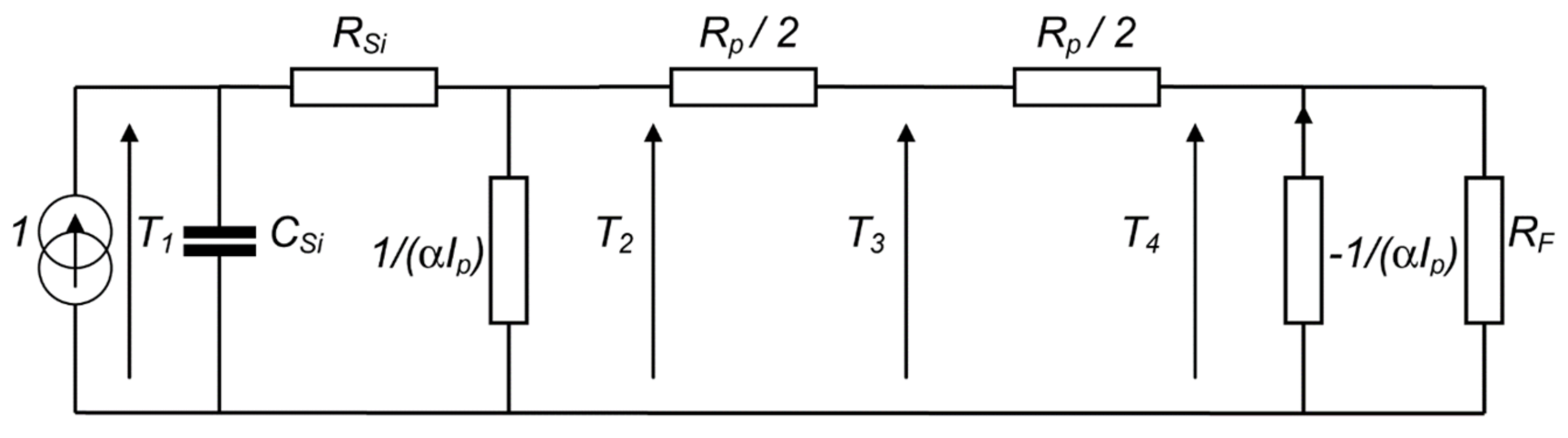
The thermal analysis of the structure, shown in Figure 2, will be performed with the help of the equivalent thermal network shown in Figure 4.
The silicon is represented by a thermal capacitance CSi and a thermal resistance RSi. The power P dissipated on the front side of the silicon, is transported through RSi to the Peltier heat pump. T is the silicon’s temperature.
The Peltier cell itself has a cold side (temperature TC) and a hot side (temperature TH). If an electric current Ip is supplied to the heat pump, the amount of heat α Ip (TC + Ta) is removed from the cold side and, similarly, the amount α Ip (TH + Ta) is fed to the hot side. α is a constant proportional to the Peltier coefficient and characteristic for a given heat pump [23]. TC + Ta is the absolute temperature of the cold side. As we are dealing in Figure 3 with a temperature rising above the ambient, the absolute value of the ambient temperature Ta has to be included in the current sources. Similarly, TH + Ta has to be used for the hot side. The Peltier cell itself also has a thermal resistance Rp between the cold and the hot side. However, the Peltier heat pump also has an electric resistance denoted by Rel. The supplied current Ip then gives rise to an additional heat generation given by RelIp2. This power is dissipated in the semiconducting part of the Peltier cell, which is located in the centre. Hence, it is most convenient to split the thermal resistance Rp into two equal parts and supply the Joule heat RelIp2 into the central node (Figure 4).
Finally, the hot side of the heat pump is cooled by a cooling fin, which can be simply represented by a thermal resistance RF (Figure 4). Note that the reference point of Figure 4 corresponds to the ambient temperature, and all temperatures shown in Figure 4 are temperature differences with respect to the ambient. This reference point is usually denoted as the “mass” in electric circuits. Only the value Ta is an absolute temperature expressed in Kelvin, as already pointed out.
In order to solve the network of Figure 4, some simplifications can be carried out. First of all, the current source α Ip (TC + Ta) can be replaced by two sources in parallel: α Ip TC and α Ip Ta. The first one, α Ip TC, delivers a current proportional to TC, which is nothing else than the temperature drop across the source. Hence, this is equivalent to the thermal resistance 1/(α Ip). In a similar way, one can handle the current source α Ip (TH + Ta). Considering that this source is oriented in the other direction, one now obtains a negative equivalent thermal resistance 1/(α Ip), as shown in Figure 5.
We are interested in finding the silicon temperature T. The easiest way to deal with the four current sources in Figure 5 is to use the well-known reciprocity theorem, which is described in many textbooks on basic network analysis.
For example, if one wants to know the influence of α IpTa on T, one has just to interchange the position of the source α Ip Ta with the source P and to detect the temperature T on the previous position of the source α Ip Ta. This gives rise to the network shown in Figure 6.
The same procedure has to be repeated for all the current sources in Figure 6. Finally, only one single (unit-valued) current source is needed, and the temperatures T1, T2, T3 and T4 have to be evaluated. The final temperature T that we are seeking is then given by the superposition:
Remark that T1, T2, T3 and T4 are temperatures for a unit power input and, hence, they are expressed in K/W and not in K. Without going into the mathematical details, the following equation is found for the temperature T [11]:
where
and
Generally, both the power P and the Peltier current Ip can be a function of the time t, depending on the proposed control mechanism. In this case, the solution of (2) can be a quite complicated mathematical expression. Therefore, we will only consider the case where the power P varies from one constant value to another one. Moreover, we assume the Peltier current Ip is a function of the power P only. Under these assumptions, (3) and (4) can be treated as constants and the expression (2) is a simple first-order differential equation with constant coefficients. If at t = 0 the power P changes from P0 (t < 0) to P1 (t > 0), the solution reads:
where T0 is the steady-state value corresponding to P0.
3. Optimal Control Strategy
The main purpose of this paper is to find a simple optimal control function Ip(P). If the power changes stepwise, the Peltier current Ip will vary accordingly. The control strategy is to keep the silicon temperature as low as possible. The value of the thermal time constant RtCSi is then no longer crucial because the maximum value of (5) either occurs at t = 0 (if the power is decreasing) or at t = ∞ (if the power is increasing). If the power dissipation in the integrated circuit increases from P0 to P1, one does not generally know how long the dissipation level P1 will last. Hence, in other words, one has no idea whether P1 will exist for a time greater than or smaller than the thermal time constant RtCSi. The only remaining criterion is to minimise the temperature value for t = ∞ or to minimise T∞.
We do not lose the generality of consideration if we assume that RSi = Rp = R and RF = βR. The condition RSi = Rp is introduced to simplify the mathematical expressions and has no impact on the conclusions. If the cooling fin is cooled by natural convection, RF >> R or β >> 1. If intensive forced convection cooling is used, it may be possible that β is close to unity or even less.
Introducing the new parameter ξ = α IpR, one obtains from (3) and (4):
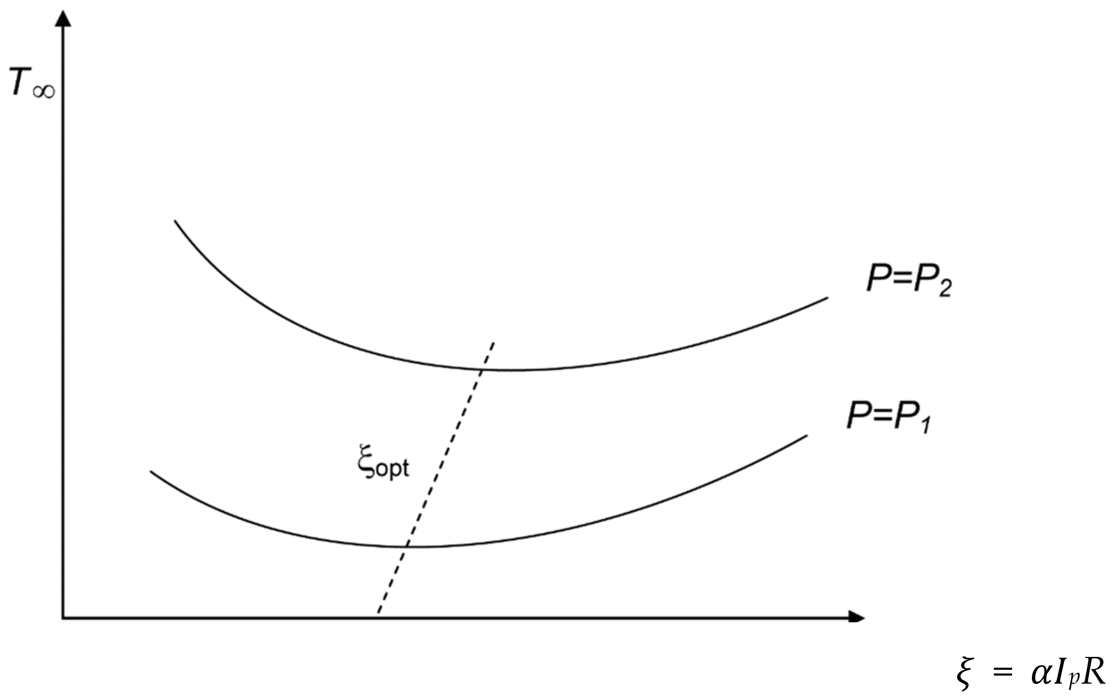
The Peltier current is, of course, quite limited. It does not make any sense to supply an excessive current Ip through a Peltier cell because the Joule heating Rel Ip2 would dominate the cooling properties of the heat pump. High values for Ip can also give rise to the unstable behaviour of the Peltier heat pump [23]. Hence, ξ = α Ip R can be considered a small parameter. One can then expand (7) in a series and neglect all terms of order ξ3 and higher:
A graphical representation of (8) is sketched in Figure 7.
For the parabolic relation (8), it is quite easy to find the point of minimum T∞:
The sketch shown in Figure 6 clearly shows the influence of the Peltier cooling as long as ξ < ξopt. As soon as ξ > ξopt, the Joule heating of the Peltier becomes too high. The latter must be avoided. Considering that the power dissipation may vary in time, one should use the optimal value ξopt corresponding to the highest power dissipation. The additional benefit of using a Peltier heat pump is that we do not have to use a separate temperature sensor to measure the chip temperature. Thanks to the Seebeck effect, the temperature can be estimated with sufficient accuracy.
One can prove that ξopt increases with the power P for β < 1. The situation β > 1 corresponds to a cooling fin with higher thermal resistance. It does not make sense to use an expensive Peltier cell where the hot side is cooled by a fin with high thermal resistance. If the dissipated power P is increased, one has to supply a higher Peltier current Ip in order to maintain the optimal cooling conditions given by (9). As can be seen from Figure 7, the variation of Ip is less than the variation of P.
For very small values of the power P, Equation (9) can be replaced by:
ξopt turns out to be a constant value. Note that for β < 1, a negative term appears in the denominator. It is then possible that ξopt can be negative as well, depending on the value of the other term. This situation looks rather cumbersome, but one should bear in mind that β < 1 corresponds to a cooling fin with a thermal resistance RF much less than the other thermal resistances. This is a common situation because the hot side of a Peltier cell has to be thermally connected to a cooling fin with small thermal resistance to the ambient air. However, if RF is extremely small, it is more convenient to connect the silicon chip directly to the cooling fin. Introducing a Peltier cell between them is then no longer helpful, as it becomes an additional thermal resistance between the silicon chip and the cooling fin.
For very high values of the power P, the relation (9) can be simplified to:
In other words, ξopt becomes a negative constant. Physically, this has no meaning. A high power implies a high Peltier current so that the Peltier power RelIp 2 is also very high or, in other words, the Peltier cell is converted into a second and unwanted heat source. Moreover, the analysis presented so far is only valid for sufficiently small values of ξ, as outlined in (8) in which terms such as ξ3 have been neglected in the series expansion.
4. Investigation Results
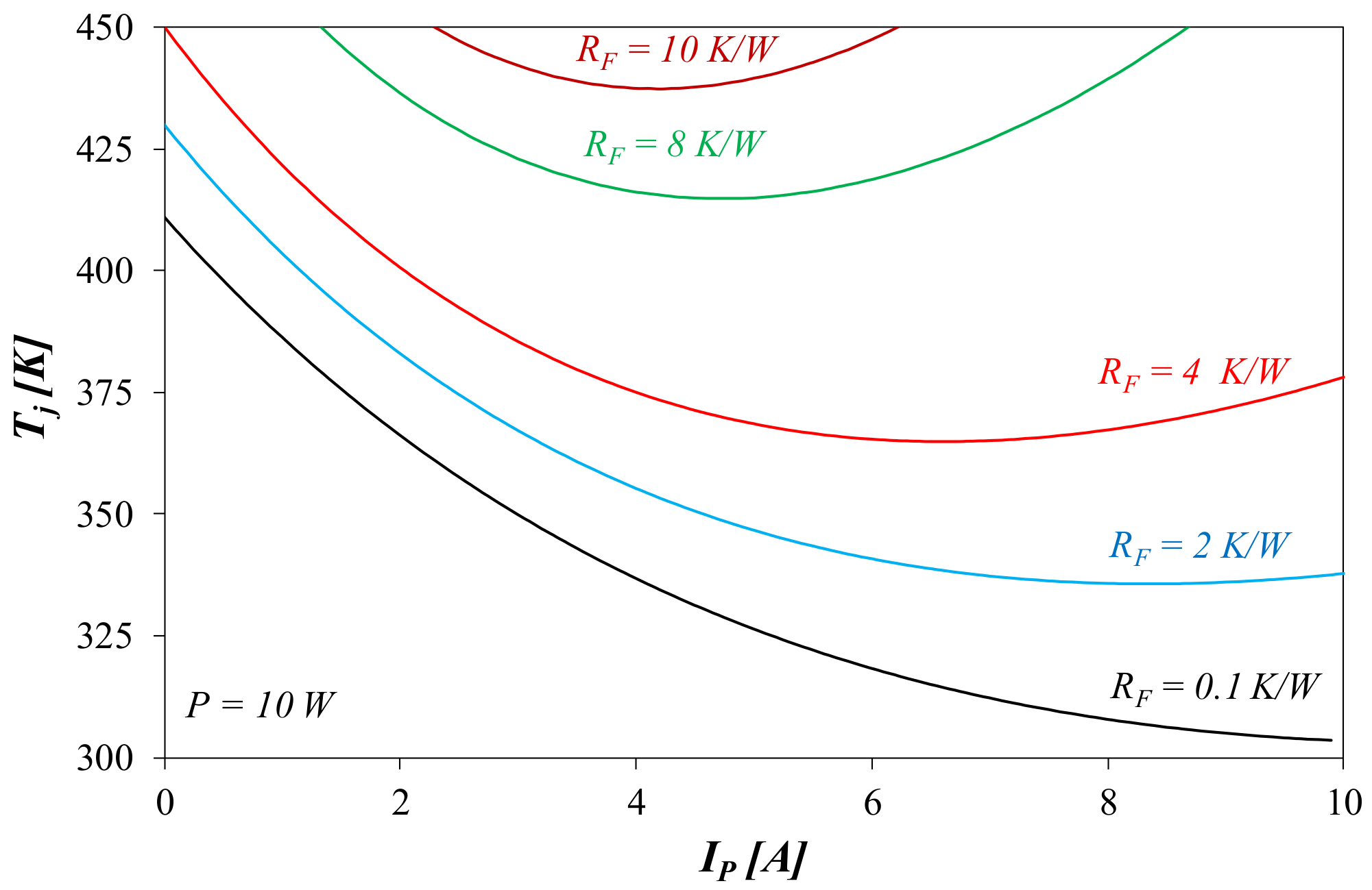
With the use of the model of the cooling system under consideration, shown in Figure 5, computer simulations were performed to illustrate the influence of selected factors on the parameters of this system. The computations were made in SPICE. The following values of the model parameters were used in the computations: α = 6.8 mV/K, Ta = 300 K, Rp = 10 K/W, RSi = 1 K/W and Rel = 0.18 Ω.
The results obtained for different values of power supply and cooling conditions of the Peltier module and for different values of the power dissipated in a cooled semiconductor device are shown in Figure 8, Figure 9, Figure 10. All these figures show the dependence of the junction temperature of the semiconductor device on the power dissipated in the cooled device (Figure 8) and the current supplying the Peltier module (Figure 9 and Figure 10).
Figure 8 shows that the obtained dependences Tj(p) are practically linear functions, and the value of the current Ip affects only the value of the slope of the relationship under consideration and the value of the temperature Tj of the device in which no power is dissipated. Due to the Peltier effect, the temperature Tj is lower than the ambient temperature Ta for low values of the power P.
Figure 9 shows that for each value of the power dissipated in the cooled device, there exists an optimal value of the current Ip at which the junction temperature of the device reaches a minimum. With an increase in the power value, the value of the current Ip, corresponding to this minimum, increases.
Figure 10 illustrates the influence of the thermal resistance RF of a heat sink on the cooling efficiency of an electronic component in a considered cooling system. It is clearly observed that an increase in the value of RF moves the minimum of the relationship Tj(Ip) to the left. This means that the use of a heat sink with high thermal resistance limits the Ip current range in which the Peltier effect can improve the cooling process of the electronic component.
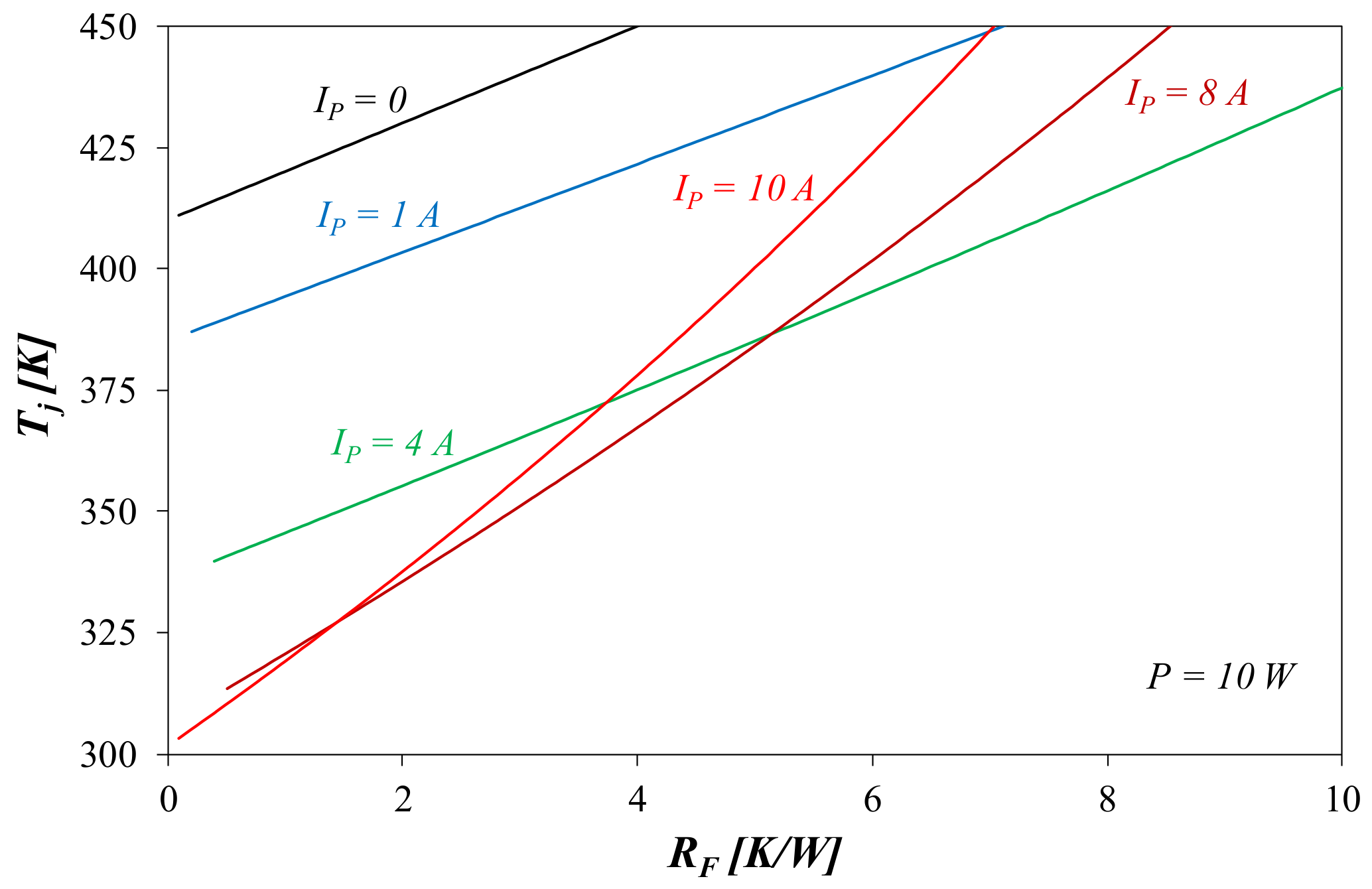
Figure 11 illustrates the influence of the Ip current on the dependence Tj(RF) at a fixed value of dissipated power P. It is easy to observe that for small values of the Ip current, the considered relationships can be described with linearly increasing functions, the slope of which decreases with an increase in this current. At high values of the Ip current, the slope of the dependence Tj(RF) is an increasing function of this current.
All the results of the computer analyses are consistent with the results of theoretical considerations presented in the previous section. Additionally, it is worth underlining that in the paper [36], many results of measurements of the cooling system containing the Peltier module, a heat sink and a fan are presented. Some of these results present measured dependences of thermal resistance and device internal temperature on the current of the Peltier module. The shape of these dependencies is the same as such results presented in Figure 10, and they possess a minimum. This agreement between shapes of measured and computed characteristics proves the correctness of the used model of the considered cooling system and the correctness of the performed theoretical considerations.
5. Conclusions
A compact thermal network model has been presented for a Peltier heat pump used for cooling a silicon integrated circuit. Using the dissipated power in the chip as the control parameter, a relation was found, providing the optimal Peltier current in order to keep the chip temperature as low as possible.
Compared with classical methods, the proposed solution does not show any time delays in response to power changes, and it is not sensitive to the position of chip temperature sensors. Moreover, it does not generate chip temperature oscillations.
Consequently, it is possible to increase the operating clock frequency and, as a consequence, an increase in the processor throughput is possible. Finally, the processor is able to operate with maximum efficiency assuming required reliability.
Because a digital processor is a part of the three-component cooling system, the mathematical and physical control process is very simple, effective and possible for implementation in every high-efficiency processor that has to be cooled.
This relation can be included in the design phase of a very high-frequency digital equipment that requires a significant amount of energy for cooling. The proposed value can be useful in the design phase of power electronics, and high-frequency processors need flexible cooling due to the high power densities.
The correctness of the theoretical considerations was confirmed with the use of computations. The shape of the obtained dependences is convergent to the results of measurements presented in the paper [36]. The conclusions presented in the previous sections may be useful for designers of electronic components cooling systems.
Author Contributions
The conceptualisation, formal analysis and methodology presented in this manuscript and their evaluation were carried out by all authors. G.D.M., A.K. and K.G. performed computer simulations, prepared figures illustrating these simulations and wrote a part of the manuscript. The funding acquisition of the financial support for the project leading to this publication was made by A.K. All authors have read and agreed to the published version of the manuscript.
Funding
The research was supported financially by the AGH University of Science and Technology, Krakow, Poland, subvention no. 16.16.230.434, and the project was financed in the framework of the programme by the Ministry of Science and Higher Education called “Regionalna Inicjatywa Doskonałości” in the years 2019–2022, project number 006/RID/2018/19.
Data Availability Statement
The data presented in this study are available on request from the corresponding author.
Acknowledgments
The authors want to express thanks to B. Wiecek for their valuable discussion.
Conflicts of Interest
The authors declare no conflict of interest.
Nomenclature
| α | Constant proportional to Peltier coefficient; characteristic for a given heat pump |
| β | Coefficient |
| ξ | Parameter |
| CSi | Thermal capacitance of silicon |
| Ip | Electric current supplied to heat pump |
| P | Power dissipated on front side of silicon |
| Rel | Electric resistance of Peltier pump |
| RF | Thermal resistance of cooling fin |
| Rp | Thermal resistance between cold and hot side of Peltier cell |
| RSi | Thermal resistance of silicon |
| T | Silicon temperature |
| Ta | Ambient temperature |
| TC | Temperature of Peltier cell, cold side |
| TH | Temperature of Peltier cell, hot side |
| Ti | Temperatures for a unit power input, i = 1, …, 4 |
References
- Jungwirth, M.; Dervić, A.; Zimmermann, H. Integrated High Voltage Active Quenching Circuit in 150nm CMOS Technology. In Proceedings of the 2020 Austrochip Workshop on Microelectronics, Vienna, Austria, 7 October 2020; pp. 53–56. [Google Scholar]
- Azar, K. The history of power dissipation. Electronics Cool. 2000, 6, 42–50. [Google Scholar]
- Lasance, C. Thermally driven reliability issues in microelectronic systems: Status-quo and Challenges. Microelectronics Reliab. 2003, 43, 1969–1974. [Google Scholar] [CrossRef]
- Frankiewicz, M.; Kos, A. Microprocessor Frequency Control Method Under Thermal and Energy Savings Constrains. IEEE Trans. Comp. Pack. Manuf. Techn. 2015, 5, 1755–1762. [Google Scholar]
- Huynh, D.; Mahjoob, Z. Numerical Analysis of Structured Ribbed Channels for Electronic Cooling Applications. In Proceedings of the 19th IEEE Intersociety Conference on Thermal and Thermomechanical Phenomena in Electronic Systems (ITherm), Orlando, FL, USA, 21–23 July 2020; pp. 766–771. [Google Scholar]
- Samake, A.; Kocanda, P.; Kos, A. Effective approach of microprocessor throughput enhancement. Microelectron. Int. 2019, 36, 14–21. [Google Scholar] [CrossRef]
- Kocanda, P.; Kos, A. Improvement of multicores throughput based on environmental conditions. Microelectron. Reliab. 2016, 60, 78–83. [Google Scholar] [CrossRef]
- Jabłoński, M.; De Mey, G.; Kos, A. Quad configuration for improved thermal design of cascode current mirror. Electron. Lett. 2012, 48, 80–82. [Google Scholar] [CrossRef] [Green Version]
- Gołda, A.; Kos, A. Optimum control of microprocessor throughput under thermal and energy saving constrains. Microelect. Reliab. 2013, 53, 582–591. [Google Scholar] [CrossRef]
- Dziurdzia, P.; Kos, A. Monitoring of power dissipated in microelectronic structures. Microelectron. Reliab. 2001, 41, 1971–1978. [Google Scholar] [CrossRef]
- Kos, A.; De Mey, G. Thermal Modelling and Optimisation of Power Microcircuits; Electrochemical Publications: Bristol, UK, 1997. [Google Scholar]
- Falsetti, C.; Amalfi, R.L.; Salamon, T.; Marcinichen, J.B.; Thome, J.R. Experimental Analysis of the Condenser Design in a Thermosiphon System for Cooling of Telecommunication Electronics. IEEE Trans. Components, Packag. Manuf. Technol. 2020, 10, 963–973. [Google Scholar] [CrossRef]
- Park, W.H.; Yang, C.K. Effects of Using Advanced Cooling Systems on the Total Power Consumption of Processors. IEEE Trans. Very Large Scale Integr. Syst. (VLSI) 2013, 21, 1644–1654. [Google Scholar] [CrossRef]
- Christen, D.; Stojadinovic, M.; Biela, J. Energy Efficient Heat Sink Design: Natural Versus Forced Convection Cooling. IEEE Trans. Power Electron. 2017, 32, 8693–8704. [Google Scholar] [CrossRef]
- Wang, C.-P. Thermal Management for Portable Electronics Using a Piezoelectric Micro-Blower. IEEE Trans. Device Mater. Reliab. 2019, 19, 563–567. [Google Scholar] [CrossRef]
- Nasab, P.S.; Perini, R.; Di Gerlando, A.C.; Foglia, G.M.M.; Moallem, M. Analytical Thermal Model of Natural-Convection Cooling in Axial Flux Machines. IEEE Trans. Ind. Electron. 2020, 67, 2711–2721. [Google Scholar] [CrossRef]
- Leon, O.; De Mey, G.; Dick, E.; Vierendeels, J. Comparison Between the Standard and Staggered Layout for Cooling Fins in Forced Convection Cooling. J. Electron. Packag. 2003, 125, 442–446. [Google Scholar] [CrossRef]
- Wei, T.; Oprins, H.; Cherman, V.; Qian, J.; De Wolf, I.; Beyne, E.; Baelmans, M. High-Efficiency Polymer-Based Direct Multi-Jet Impingement Cooling Solution for High-Power Devices. IEEE Trans. Power Electron. 2019, 34, 6601–6612. [Google Scholar] [CrossRef]
- Jorg, J.; Taraborrelli, S.; Sarriegui, G.; De Doncker, R.W.; Kneer, R.; Rohlfs, W. Direct Single Impinging Jet Cooling of a mosfet Power Electronic Module. IEEE Trans. Power Electron. 2018, 33, 4224–4237. [Google Scholar] [CrossRef]
- Legierski, J.; Więcek, B.; De Mey, G. Measurements and simulations of transient characteristics of heat pipes. Microelectron. Reliab. 2006, 46, 109–115. [Google Scholar] [CrossRef]
- Zweben, C. Revolutionary new thermal management materials. Electronics Cooling 2005, 11, 36–37. [Google Scholar]
- Wang, J.; Li, H.; Cho, E.Y.; Lefebvre, J.C.; Pratt, K.; Cybart, S.A. Portable Solid Nitrogen Cooling System for High Transition Temperature Superconductive Electronics. IEEE Trans. Appl. Supercond. 2020, 30, 1–3. [Google Scholar] [CrossRef]
- Vermeerscn, N.; De Mey, G. Influence of substrate thickness on thermal impedance of microelectronic structures. Microelectron. Reliab. 2007, 47, 437–443. [Google Scholar] [CrossRef] [Green Version]
- De Baetselier, E.; Goedertier, W.; De Mey, G. A survey of the thermal stability of an active heat sink. Microelectron. Reliab. 1997, 37, 1805–1812. [Google Scholar] [CrossRef]
- Vermeersch, B.; De Mey, G. A Fixed-Angle Dynamic Heat Spreading Model for (An)Isotropic Rear-Cooled Substrates. J. Heat Transf. 2008, 130, 121301. [Google Scholar] [CrossRef]
- Zhu, H.; Hu, F.; Zhou, H.; Pan, D.Z.; Zhou, D.; Zeng, X. Interlayer Cooling Network Design for High-Performance 3D ICs Using Channel Patterning and Pruning. IEEE Trans. Comput. Des. Integr. Circuits Syst. 2018, 37, 770–781. [Google Scholar] [CrossRef]
- Wang, N.; Shen, Z.-H.; Gao, C.; Chen, M.-M.; Ding, C.; Sui, G.-R.; Jia, H.-Z.; Gao, X.-M. Electrothermal Collaborative Cooling with Delayed Power Rail Switching Auxiliary Charging by Conservation Energy Harvesting Mechan for High-Power LEDs. IEEE Trans. Comp. Pack. Manuf. Techn. 2020, 10, 1507–1514. [Google Scholar]
- Pan, Y.; Li, J.; Wang, W.; Ye, T.; Yin, H.; Huang, K.; Zhang, Z.; Zhang, Q.; Jia, K.; Wu, Z.; et al. Novel 10-nm Gate Length MoS2 Transistor Fabricated on Si Fin Substrate. IEEE J. Electron Devices Soc. 2019, 7, 483–488. [Google Scholar] [CrossRef]
- Raszkowski, T.; Samson, A.; Zubert, M.; Janicki, M. Comparison of temperature distributions in modern nanostructures based on different parameters of Dual-Phase-Lag equation. In Proceedings of the 2018 IEEE 20th Electronics Packaging Technology Conference (EPTC), Singapore, 4–7 December 2018; pp. 290–295. [Google Scholar] [CrossRef]
- Raszkowski, T.; Samson, A.; Zubert, M.; Janicki, M.; Napieralski, A. The numerical analysis of heat transfer at nanoscale using full and reduced DPL models. In Proceedings of the 2017 18th International Conference on Thermal, Mechanical and Multi-Physics Simulation and Experiments in Microelectronics and Microsystems (EuroSimE), Dresden, Germany, 3–5 April 2017; pp. 1–6. [Google Scholar] [CrossRef]
- Nolas, G.S.; Sharp, J.; Goldsmid, H.J. Thermoelectric: Basic Principles and New Materials Developments; Springer-Verlag: Berlin/Heidelberg, Germany, 2001. [Google Scholar]
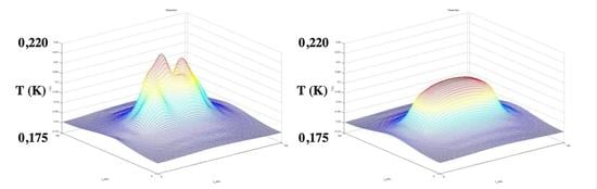
- Posobkiewicz, K.; Górecki, K. Influence of selected factors on thermal parameters of the components of forced cooling systems of electronic devices. Electronics 2021, 10, 340. [Google Scholar] [CrossRef]
- Moduły Peltiera. Available online: https://sklep.semicon.com.pl/shop2/moduly-peltiera,c1197?gclid=EAIaIQobChMIs_Tr2My87gIVg-d3Ch1L_gmmEAAYASAAEgJ1K_D_BwE (accessed on 8 January 2022).
- Moduł Peltiera Do chłoDzenia Termoelektrycznego, Typu Direct-to-Air, 24.9 W, 2.3 A. MPDT-AR-024-12. Available online: https://pl.farnell.com/multicomp-pro/mpdt-ar-024-12/peltier-module-24-9w-80-x-63-3/dp/3267537?gclid=EAIaIQobChMIs_Tr2My87gIVgd3Ch1L_gmmEAQYBSABEgJnWfD_BwE&gross_price=true&mckv=sfPiU03yp_dc|pcrid|459813550005|plid||kword||match||slid||product|3267537|pgrid|109028182753|ptaid|pla-299936849176|&CMP=KNC-GPL-SHOPPING-Whoop-ME-31-Aug-20 (accessed on 8 January 2022).
- Moduł Peltiera. Available online: https://pl.farnell.com/multicomp-pro/mp-ar-ar-040-24/peltier-module-37w-400-x-189-5/dp/3267541?st=ch%C5%82odzenie (accessed on 8 January 2022).
- Posobkiewicz, K.; Górecki, K. Influence of selected factors on parameters of a cooling system with a Peltier module and forced air flow. Microelectron. Int. 2022. Ahead of print. [Google Scholar] [CrossRef]
Figure 1.
(a) Singular Peltier cell (n,p—semiconductors, e.g., Be2Te3); (b) classical feedback loop in active heat sink control system.
Figure 1.
(a) Singular Peltier cell (n,p—semiconductors, e.g., Be2Te3); (b) classical feedback loop in active heat sink control system.

Figure 2.
Chip–Peltier heat pump—cooling fin structure.

Figure 3.
Examples: (a) multi-cell Peltier heat pumps [33]; (b) Peltier heat pump with cooling fin [34]; (c) Peltier heat pump with cooling fin and fan [35].

Figure 4.
Equivalent thermal network for the structure of Figure 2.
Figure 4.
Equivalent thermal network for the structure of Figure 2.

Figure 5.
Simplified equivalent network.

Figure 6.
Network in relation to the reciprocity theorem.

Figure 7.
Temperature versus the parameter ξ.

Figure 8.
Device junction temperature versus power dissipated at selected values of the current Ip.

Figure 9.
Device junction temperature versus the current Ip at selected values of power dissipated.

Figure 10.
Device junction temperature versus the current Ip at selected values of fins thermal resistance.
Figure 10.
Device junction temperature versus the current Ip at selected values of fins thermal resistance.

Figure 11.
Device junction temperature versus the fin thermal resistance at selected values of current IP.
Figure 11.
Device junction temperature versus the fin thermal resistance at selected values of current IP.

Publisher’s Note: MDPI stays neutral with regard to jurisdictional claims in published maps and institutional affiliations. |
© 2022 by the authors. Licensee MDPI, Basel, Switzerland. This article is an open access article distributed under the terms and conditions of the Creative Commons Attribution (CC BY) license (https://creativecommons.org/licenses/by/4.0/).
Share and Cite
MDPI and ACS Style
De Mey, G.; Kos, A.; Górecki, K. Optimal Temperature Regulation of Integrated Circuits with Peltier Heat Pumps. Energies 2022, 15, 1125. https://0-doi-org.brum.beds.ac.uk/10.3390/en15031125
AMA Style
De Mey G, Kos A, Górecki K. Optimal Temperature Regulation of Integrated Circuits with Peltier Heat Pumps. Energies. 2022; 15(3):1125. https://0-doi-org.brum.beds.ac.uk/10.3390/en15031125
Chicago/Turabian StyleDe Mey, Gilbert, Andrzej Kos, and Krzysztof Górecki. 2022. "Optimal Temperature Regulation of Integrated Circuits with Peltier Heat Pumps" Energies 15, no. 3: 1125. https://0-doi-org.brum.beds.ac.uk/10.3390/en15031125
Note that from the first issue of 2016, this journal uses article numbers instead of page numbers. See further details here.