


Power Conversion Interface for a Small-Capacity Photovoltaic Power Generation System
1
Department of Microelectronic Engineering, National Kaohsiung University of Science and Technology, Kaohsiung City 81157, Taiwan
2
Department of Electrical Engineering, National Kaohsiung University of Science and Technology, Kaohsiung City 807618, Taiwan
*
Author to whom correspondence should be addressed.
Energies 2023, 16(3), 1097; https://0-doi-org.brum.beds.ac.uk/10.3390/en16031097
Submission received: 3 January 2023
/
Revised: 6 January 2023
/
Accepted: 18 January 2023
/
Published: 19 January 2023
(This article belongs to the Special Issue Advances in Power Electronic Converters with Application in Renewable Energy Sources)
Abstract
:A power conversion interface for a small-capacity photovoltaic power generation system (PPGS) is proposed in this paper. The proposed power conversion interface is composed of a DC–DC converter (DDC), a battery pack and a buck–boost inverter (BBI). The battery pack is integrated to the power conversion interface to store or release energy for smoothing the power fluctuation of the small-capacity PPGS. The battery pack is only activated when a large power change occurs in the photovoltaic array (PV array). The DC power, no matter whether is from the PV array or the battery pack, needs to be converted into AC power only by the BBI in the proposed power conversion interface. Moreover, the PV array charges the battery pack only through the DDC, which simplifies the power circuit and improves the power conversion efficiency. To verify the feasibility of the proposed power conversion interface, a hardware prototype is established for practical experiments.
1. Introduction
Climate change sounds the alarm for global carbon reduction. Many countries have successively put forward the declaration of “2050 net zero emissions”. Renewable energy power generation technologies, which are effective ways to reduce gas emissions in power generation, draw more and more attention. Both commercial and residential renewable power generation help to increase the penetration of renewable energy. Among those mature renewable energy power generation technologies, photovoltaic energy is appropriate for residential applications with restricted space. The photovoltaic power conversion interface for small-capacity systems is just as crucial as the one for larger-capacity systems.
The output of the photovoltaic array (PV array) is DC power, while the dominant power grids are AC power systems. Hence, an inverter is required to interface the PV array and the power grid [1,2,3,4,5,6]. Limited by space, small-capacity photovoltaic power generation system (PPGS) uses fewer PV modules with low output voltage. The conventional full-bridge inverter (FBI) is a step-down conversion architecture, and the DC bus voltage must be higher than the amplitude of the power grid voltage. Therefore, a boost power converter is added in the conventional small-capacity PPGS with an FBI to boost the output voltage of the PV array to be higher than the amplitude of the power grid voltage [1,2,3]. It indicates that two power stages (PSs) are required for power conversion in a conventional small-capacity PPGS with an FBI. One is a boost converter for tracking the maximum power point and boosting output voltage of PV array and the other is an inverter used for DC to AC power conversion. On the one hand, it has the advantage that each PS is independent to achieve the optimal control design. On the other hand, its reliability is reduced and both the cost and the volume are increased. In addition, the power of PV array is processed through two PSs, resulting in low power efficiency. For reducing the number of PSs of the small-capacity PPGS, several inverters with step-up and step-down functions have been proposed. In order to perform step-up/down power conversion architecture, the filter inductor is moved to the DC side of the FBI in a Z-source inverter [5,6,7,8,9]. The input DC voltage can be lower than the amplitude of the power grid voltage, thereby eliminating the need for a boost power converter. However, the control is more complicated. In [10,11], an inverter, integrated by two boost power converters, is proposed. Each boost power converter generates a voltage that consists of a sinusoidal voltage and a DC offset. The difference between the output voltages of the two boost power converters is the output voltage of the inverter, resulting in a sinusoidal voltage. Nevertheless, the output voltages of both boost power converters contain a DC offset, which results in high switching power losses. A new family of single-stage buck–boost inverters with an unfolding circuit is proposed in [12,13]. A bidirectional buck–boost converter is integrated to the DC bus of the FBI. The bidirectional buck–boost converter generates an absolute grid current, and the unfolding FBI is used for commutation to supply AC current. However, all power from the DC source to the grid is converted through the inductor, which reduces the power efficiency. In [14], a three-phase tri-state buck–boost integrated inverter for solar applications is developed. A power electronic switch and an inductor convert the dc voltage to a current, and a current-source FBI is used to generate three-phase currents injected into the power grid. However, all power generated by the PV array must first be converted to the power stored in the inductor and then to the power grid, reducing power efficiency. In addition, the three-phase tri-state buck–boost integrated inverter cannot supply reactive power. A state-of-the-art survey for the buck–boost inverters (BBIs) is provided in [15]. The above topologies are used for applications with a single DC source. A dual-input BBI is proposed in [16] to process the output powers of two DC sources. However, the dual-input BBI cannot provide reactive power.
Solar power penetration increases with the decreasing cost of photovoltaic modules. Significant changes in the output power of PPGSs cause fluctuations in grid voltage and deviations in grid frequency as a result of changes in the solar illumination radiation. In order to smooth the power generated from the PPGS, how to suppress the fluctuation of the output power that is fed into the power grid has received much attention [6,17,18,19,20,21]. There are two methods to suppress the fluctuation in the power generated from the PPGS. One is to adjust the maximum power point tracking (MPPT) [17]. The output power of a PPGS can only be controlled by this approach in terms of the rate of growth; it cannot regulate the rate of decrease. The other is to use an energy buffer to smooth the power generated by the PPGS. A battery pack is well suited to serve as an energy buffer due to its benefits of high energy density and high charging/discharging rate [17,18,19,20,21]. A battery pack supplies the power difference between the average power and the instantaneous power output from the PV array. The average power output from the PV array can be obtained either by the low-pass filters [17,18,19,20], or by the moving average filters [18,19,22]. However, the required capacity of the battery pack is different due to the different delay of the filters. The power structure of the conventional PPGS with a battery energy storage system is shown in Figure 1 [22,23]. The PV array and the battery pack are, respectively, connected to the DC bus of the inverter through two DC–DC converters (DDCs). The power processing flow in between the PV array, the battery pack and the power grid is always handled by two PSs. Because multiple power converters are used in the PPGSs with the battery pack, the conversion efficiency is reduced and the power circuit is complicated. In [24], the battery pack is directly connected to the DC bus of the inverter. One DDC is saved, but utilization of battery pack is limited.
The power conversion interfaces of PPGS are still an important research issue in terms of simplifying power circuits and smoothing output power and power efficiency. This paper proposes a power conversion interface for a small-capacity PPGS. It is composed of a BBI, a DDC and a battery pack. The BBI integrates a boost stage and a buck-commutation stage. Although the topology of a BBI is similar to that of a conventional small-capacity PPGS, the modulation and control strategy is modified and either the boost stage or the buck-commutation stage is switching at a time. Hence, the proposed BBI combines the operation of two PSs in the conventional small-capacity PPGS, such that only one PS is used to convert the DC power from the PV array or the battery pack to the AC power injected into the power grid. Therefore, the conversion efficiency of the PPGS is improved. In addition, the battery pack is integrated to smooth the output power of the PPGS. The output power of the PPGS changes within a slope limitation when the power difference between the PV array and the PPGS exceeds the setting range. It requires no filter with a low cut-off frequency to obtain average power, which reduces the compensation capacity of the battery pack. The battery energy storage system can be integrated into the PPGS by only adding an additional DDC. In addition, the charging power of the battery pack is converted from the PV array by only one PS. Compared with the conventional PPGS, combined with a battery energy storage system shown in [22,23], the proposed topology is simplified and the conversion efficiency is improved.
This paper is organized as follows. In Section 2, the circuit configuration and operation principle of the power conversion interface are presented. In Section 3 and Section 4, the operations and control blocks of the BBI and DDC are addressed. In Section 5, the prototype is built and experimental results are provided to verify the performance of the proposed power conversion interface. Finally, Section 6 provides some conclusions.
2. Circuit Configuration and Operation Principle
The power circuit of the proposed power conversion interface for a small-capacity PPGS is shown in Figure 2. The proposed power conversion interface is composed of a DDC, a battery pack and a BBI. The battery pack is integrated to the power conversion interface to store or release energy to smooth the output power of the PPGS. From Figure 2, it can be seen that the input DC source of the BBI can be selected from the PV array or the battery pack. Considering the power flow, the operation of the proposed power conversion interface can be divided into three modes, as shown in Figure 3.
- Mode I:
In this mode, the change rate for the output power of the PV array is within the setting range, and the state of charge (SOC) of the battery pack is at the setting value. The power flow is shown in Figure 3a. The input DC source of the BBI is the PV array, and the battery pack is disabled. The MPPT of the PV array is performed by the BBI.
- Mode II:
There are two situations in this mode. One is that the change rate for the output power of the PV array is above the upper limit of the setting range. The other is that the change rate for the output power of the PV array is within the setting range, but the SOC of the battery pack is below the setting value. The power flow is shown in Figure 3b. The input source of the BBI is the PV array. The BBI adjusts the change rate for the output power of the PPGS within the setting range. The battery pack is charged by the PV array through the DDC to share the power difference between the PV array and the PPGS. The MPPT of PV array is performed by the DDC.
- Mode III:
This mode includes two situations. One is that the change rate for the output power of PV array is below the lower limit of setting range. The other is that the change rate for the output power of the PV array is within the setting range but the SOC of the battery pack is above the setting value. The power flow is shown in Figure 3c. The input source of the BBI is the battery pack. The BBI adjusts the change rate for the output power of PPGS within the setting range. The battery pack is discharged to supply the power difference between the PV array and the PPGS. The DDC performs the MPPT of PV array.
3. Operation and Control of Buck–Boost Inverter
As shown in Figure 1, the BBI is composed of a boost stage and a buck-commutation stage and a buck/boost selection switch S2. The boost stage includes the power electronic switch S1, the inductor L1, the diode D1 and the capacitor C2, and the buck-commutation stage is configured by the power electronic switches (S3, S4, S5, S6), the inductor LS and the capacitor CS.
Figure 4 shows the time diagram for the operation principle of the BBI. The operation mode is determined by comparing the absolute power grid voltage |VS| and the input DC voltage VDC. The input DC voltage is the voltage of the PV array or the voltage of the battery pack. The BBI operates in the buck mode when VDC is greater than |VS|. At this mode, the boost/buck selection switch S2 is turned on, and the boost stage is disabled. S3 and S4 of the buck-commutation stage are switched in high-frequency pulse-width modulation (PWM) to perform the buck operation, and S5 and S6 are switched at low frequency according to the polarity of the power grid voltage to achieve the commutation function. On the contrary, when VDC is less than |VS|, the BBI operates in boost mode. At this mode, the boost/buck selection switch S2 is turned off. S1 of the boost stage is switched in high-frequency PWM to perform the boost operation and S3-S6 of the buck-commutation stage perform the commutation function according to the polarity of the power grid voltage. When the operation is switched from the boost mode to the buck mode, the boost/buck selection switch S2 is not immediately turned on because the current of inductor L1 of the boost stage is not zero. Otherwise, the residual current of inductor L1 will circulate between D1 and the boost/buck selection switch S2, resulting in an additional loss. The boost/buck selection switch S2 is turned on when the current of inductor L1 drops to zero. The operation of different time intervals in the positive-half cycle for the BBI is described as follows:
- [t0-t1] and [t3-t4]:
In these time intervals, VDC is greater than |VS|. The BBI is operated in the buck mode. The buck-commutation stage is operated, and the boost stage is disabled. Assuming that the current of the inductor LS is continuous conducting, the relationship between VDC and the power grid voltage is
where DS3 is the duty cycle of S3. The current of inductor LS can be controlled to increase/decrease to track the reference current by switching S3 and S4.
- [t1-t2]:
In this time interval, VDC is less than |VS|. The BBI is operated in the boost mode. The boost stage is activated, and the buck-commutation stage performs the commutation function. The output current of the boost stage is the current of D1 (iD1), which is a discontinuous current. Therefore, a third-order low-pass filter is formed by using the capacitor C2, the inductor LS and the capacitor CS to filter out the high-frequency components of iD1. The capacitor C2 and the inductor LS form a second-order low-pass filter for the power grid voltage. Because the cut-off frequency of second-order low-pass filter is much higher than the frequency of the power grid voltage, the voltage across the capacitor C2 is approximate to |VS|. If the current of inductor L1 is continuous conducting, the relationship between the input DC voltage and the power grid voltage is
where DS1 is the duty cycle of S1. By controlling the switching of S1, the current of inductor L1 can be controlled to increase/decrease. Thereby, it regulates the output current to track the reference current.
- [t2-t3]:
In this time interval, VDC is greater than |VS|. During this interval, the boost stage would have to stop operating and switch to the buck-commutation stage. However, if the power electronic switch S2 is turned on, the voltage of the inductor L1 is almost zero, which makes the current of inductor L1 almost unchanged. This current will form a circulating current in the circuit and cause additional power loss. Therefore, there must be a transition period when the operation is switched from the boost mode to the buck mode. In this time interval, the boost stage is disabled, and the buck-commutation stage is operated but the power electronic switch S2 must be turned off. Because the boost stage is disabled, the current of the inductor L1 is still decreased. The current of inductor LS can be controlled to increase/decrease to track the reference current by switching S3 and S4.
The operation of BBI in the negative half cycle is similar to that in the positive half cycle, and will not be repeated. The power electronic switches of BBI are controlled according to the comparison between VDC and |VS|, and the operation of power electronic switches is summarized in Table 1.
The circuit structure of the BBI is similar to that of the conventional small-capacity PPGS consisting of a boost power converter and an FBI; however, the operation and the control for both circuit structures are different. Both the boost power converter and the FBI are operated simultaneously in the conventional small-capacity PPGS. In the proposed approach, the boost stage or the buck-commutation stage is switching at a time. Hence, the input DC power is processed by one PS in the BBI but two PSs in the conventional small-capacity PPGS. In addition, the BBI can avoid a large-capacity electrolytic capacitor, working as an energy buffer between the boost power converter and the FBI, in the conventional small-capacity PPGS. Therefore, the power efficiency will be improved by using the BBI to replace both the boost power converter and the FBI used in the conventional small-capacity PPGS.
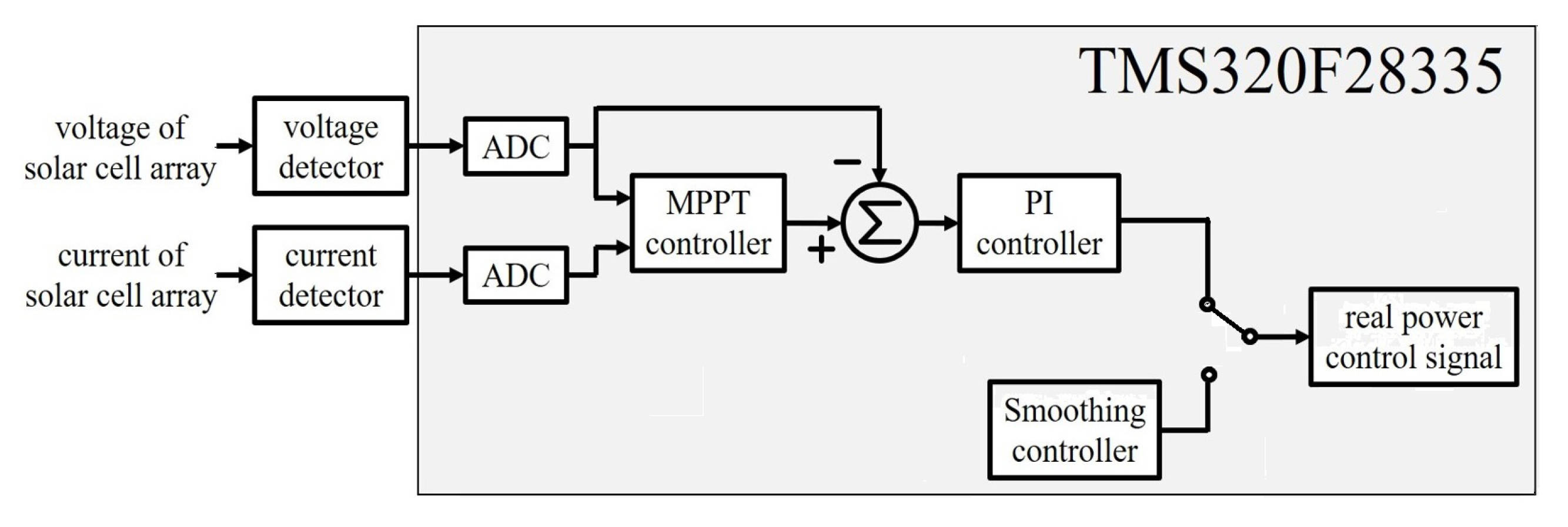
Figure 5 shows the control block of the BBI. In order to generate a sinusoidal current synchronized with the power grid voltage, the BBI adopts a current-mode control and feedforward control to adjust the current of the inductor L1 and the current of the inductor LS. The controller is implemented by a digital signal processor (DSP) TMS320F28335, and the program is written in C programming language. The power grid voltage is detected and then sent to a phase lock loop (PLL). A sine-wave table is used to generate two orthogonal sinusoidal signals that are in phase and shifted by 90 degrees with the power grid voltage. The real power control signal and the reactive power control signal are multiplied by two sinusoidal signals, respectively, to generate reference currents of the real power and the reactive power. Then, they are added to obtain a reference current of the output current. Since the control object of the boost stage is the current iL1, and the output current of the boost stage approaches the current of diode D1. Hence, the reference current of iL1 can be represented as
where DS1 is the duty of S1. Therefore, the reference current of iL1 must be calculated by the reference current . The current iL1 is detected and subtracted from the reference current , and the error is sent to the current controller (controller I) to generate the current control signal of boost mode. The current of inductor Ls is detected and subtracted from the reference current , and the error is sent to the current controller (controller II) to obtain the current control signal of buck mode. The feedforward signals of boost mode and buck mode are
where Vtri is the peak value of the carrier signal of PWM. The feedforward signals of boost mode and buck mode are, respectively, added to the current control signals of boost mode and buck mode to generate a boost modulation signal and a buck modulation signal. The boost modulation signal mbo and the buck modulation signal mbu are sent to the logic and PWM circuit to generate the switching signals for S1-S6. The feedforward signals of boost mode and buck mode will generate a major part of the modulation signals. Current mode controls in the boost mode and the buck mode are only used to fine-tune the modulation signals, so the current controller I and the current controller II use proportional control. The gains of the current controller I and the current controller II are used to fine-tune the total harmonic distortion (THD) of output current.
The real power control signal is determined by either the MPPT control or the smoothing control of the PV array, and its control block is shown in Figure 6. When the change rate of the output power of the PV array is within the setting range (P1, -P1) and the SOC of the battery pack is equal to the setting value, the real power control signal is determined by the MPPT control of the PV array. Otherwise, the real power control signal is obtained from the smoothing control. The MPPT controller uses the perturbation and observation (P & O) method to calculate a reference voltage [25]. The reference voltage is subtracted from the voltage of the PV array, and the result is sent to the PI controller to generate an MPPT signal Imp. When the smoothing control is activated, the smoothing controller generates a smoothing signal Ism with a constant rising slope or a constant falling slope. The real power control signal is generated by Imp or Ism through a selection switch, and the control of the selection switch is generated by comparing the difference power between the PV array and the PPGS with the setting range (P1, -P1).
Figure 7 shows the block of logic and the PWM circuit. The purpose of S5 and S6 is used for the commutation operation, so the power grid voltage is compared with zero voltage to generate the control signals for S5 and S6. The operation mode is determined by comparing |VS| with VDC. VDC is the voltage of the PV array or the battery pack, which is determined by the operation mode shown in Figure 3. When |VS| is greater than VDC, the boost operation signal fbo is high. When |VS| is less than VDC, the buck operation signal fbu is high. The buck modulation signal mbu and the boost modulation signal mbo are, respectively, compared with the carrier signal to generate the buck PWM signal and the boost PWM signal. S3 and S4 are switched in PWM under the buck mode and participate in the commutation operation under the boost mode. S1 is switched in PWM under the boost mode. In order to prevent the residual current of the inductor L1 when the operation is switched from the boost mode to the buck mode, the result of comparing IL1 with zero and fbu are sent to a AND gate to control S2.
Figure 8 and Figure 9 are the results simulated by the PSIM program. Figure 8 shows the voltage waveforms of S1 and S3 in a power grid cycle. The power grid is a single-phase voltage source of 110 V, 60 Hz. The input is a DC voltage source of 90 V. The DC bus voltage of an FBI in a conventional PPGS is set between 180 V and 200 V. As can be seen in Figure 8b,c, S1 is only switching in boost mode. The switching voltage is about |VS| which is less than the DC bus voltage of the FBI in the conventional PPGS. Because the switching loss is proportional to the switching voltage, the switching loss is reduced. In addition, S1 is still turned off in buck mode. Therefore, the switching loss of the boost stage is significantly reduced compared with that of a boost converter in the conventional PPGS. From Figure 8d,e, in buck mode, when S3 switches at high frequency, the voltage stress of S3 is around the input DC voltage which is less than the DC bus voltage of the FBI in the conventional PPGS. In the boost mode, S3 switches at low frequency. Therefore, the switching loss of the buck-commutation stage is lower than that of the FBI in the conventional PPGS. Figure 9 shows the voltages across the LS and L1 in a power grid cycle. The current ripple is proportional to the voltage swing across the inductor. From Figure 9, it can be seen that the voltage swings across L1 and LS are less than that in the conventional PPGS. Therefore, the inductances of L1 and LS can be reduced.
4. Operation and Control of DC–DC Converter
As shown in Figure 2, the DDC is a boost converter. In Figure 3, it can be found that the DDC will be operated to perform the MPPT function and to charge the battery pack when the output power of the PV array changes significantly. Figure 10 shows the control block of the DDC. The DDC adopts the voltage control. The control object is the output voltage of the PV array to track the maximum power point of the PV array. The MPPT controller calculates a reference voltage signal and subtracts it from the output voltage of the PV array. The result is sent to the PI controller to generate a modulation signal, and then sent to the PWM circuit to control S7. S7 switches when the power conversion interface is operated in modes II and III, as shown in Figure 3. The control of S8 is actuated when the power conversion interface is operated in mode III, as shown in Figure 3.
5. Experimental Results
A hardware prototype has been developed to verify the performance of the proposed power conversion interface. The battery pack is composed of ten 12 V lead-acid batteries connected in series. The capacity of the lead-acid batteries is 14 Ah. The solar simulator is used to simulate a PV array with three solar modules, and the open-circuit voltage and short-current current of each solar module are 38.08 V and 8.65 A, respectively. The output of the power conversion interface is connected to a single-phase power grid of 60 HZ and 110 V. Table 2 shows the circuit parameters of the hardware prototype. Figure 11 shows the picture of the prototype. The prototype is composed of a power supply board, a DSP board, a driver board, a voltage detection board, a current detection board and power boards of DDC and BBI.
In order to facilitate the experimental verification of the BBI, the PV array is replaced by a DC power supply. Figure 12 shows the experimental results of the BBI at a steady state. The output current is a sine wave and in phase with the power grid voltage. The THD of the output current is 3.2%. When the BBI operates in the boost mode, the current of inductor L1 is 1/(1-DS1) times the output current. The boost stage does not operate and the current of inductor L1 will drop to zero in the buck mode. It verifies that the BBI can reduce the current of inductor L1 to zero to avoid circulating the current when the operation is switched from the boost mode to the buck mode. The BBI can simultaneously adjust the amplitude and phase of the output current during power conversion. Figure 13 and Figure 14 show the experimental results of the BBI for providing reactive power. As can be seen, the output current can be leading or lagging to the power grid voltage. The THD of the output current is slightly increased to about 5% when the BBI provides reactive power. The experimental results prove that the BBI has the ability to simultaneously adjust the reactive power while converting the real power of input DC source.
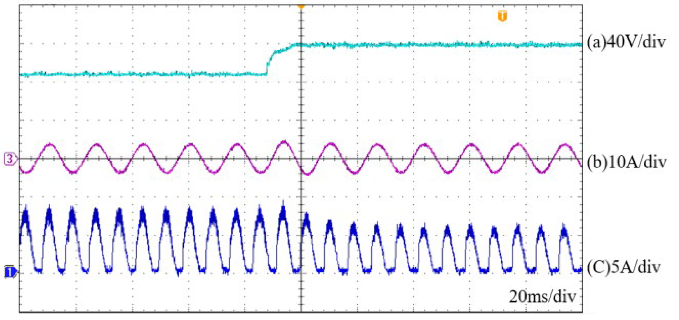
Figure 15 shows the experimental results of the BBI under the transient of the input DC voltage variation. Figure 15a shows that the input DC voltage rises from 90 V to 120 V. Since the output power remains unchanged, the output current of Figure 15b is still sinusoidal and remains unchanged. As shown in Figure 15c, when the input voltage rises, the BBI operates in the buck mode for a longer time, so the current of inductor L1 becomes smaller. The experimental results demonstrate that the BBI has a good transient response under the change of input DC voltage.
Figure 16 shows the power efficiency of the conventional small-capacity PPGS. The power efficiency is calculated by using two Tektronix PA 100 power analyzers to measure the input power and output power of the BBI. The conventional small-capacity PPGS is modified by the prototype of BBI. The power electronic switch S2 is still off and the capacitor C2 is replaced by a large-capacity electrolytic capacitor. The DDC is still operated to supply a DC bus voltage to the FBI. The FBI is operated to generate a sinusoidal current injected to the power grid. Figure 17 shows the power efficiency of the BBI. The topology of the BBI is similar to that of the conventional small-capacity PPGS, however, the boost stage or the buck-commutation stage is switching at a time. Hence, the DC power from the PV array or the battery pack is converted to AC power through only one PS, and the buck-commutation stage operates at a lower DC-link voltage. It can be seen from Figure 16 and Figure 17 that the power efficiency of the BBI is better than that of the conventional small-capacity PPGS. In addition, the BBI can effectively reduce the capacitance of capacitor C2, reducing the circuit volume and circuit cost.
The DC power supply was replaced by the solar simulator to verify the MPPT function of the BBI. In order to verify the MPPT function, firstly it is necessary to scan the power of the solar simulator. The output voltage of the solar simulator is changed from low to high, and the output power scan for the solar simulator is shown in Figure 18a. As can be seen, the maximum power is 552 W. Figure 18b shows the experimental result for the maximum power tracking of the BBI. As can be seen, the output power of the solar simulator slowly rises at the beginning. When the output power of the solar simulator reaches the maximum power point, it fluctuates near the maximum power point. The maximum power of Figure 18b is 550 W, which approaches to the maximum power in Figure 18a. The experimental results prove that the BBI has the ability to track the maximum power point of the solar simulator.
Figure 19 shows the experimental results when the smoothing mechanism is activated. The output power of the solar simulator is 500 W at the beginning of the measurement. After time t1, the illumination changes drastically to simulate the cloud movement, and the output power of the solar simulator also changes accordingly. From Figure 19b, the output power of the PPGS changes at a constant slope when the power difference between the solar simulator and the PPGS exceeds the setting range. At the same time, the battery pack must start charging/discharging to provide the power difference between the solar simulator and the PPGS. The power of battery pack is shown in Figure 19c. The battery pack is only used to smooth the output power of PPGS. Hence, the output power of PPGS fluctuates when the output power of the PV array is changed significantly. The slope of the output power of the PPGS when the output power of the PV array is changed significantly can be modified according to the standards of different countries. The slope affects the design of the capacity of the battery pack. The experimental results verify that the proposed power conversion interface can effectively attenuate the power fluctuation of the PV array. Therefore, the PPGS provides more stable power to the power grid.
6. Conclusions
The instability of the power generation of the PPGS will affect the power quality of the power grid. A power conversion interface, integrating a DC–DC boost power converter, a battery pack and a BBI, is proposed for a small-capacity PPGS. When compared with the conventional small-capacity PPGS, the proposed small-capacity PPGS has the following advantages:
- The output power of the PV array or the battery pack is processed by only one PS, and the power efficiency is improved.
- Only one extra DDC is added to integrate the battery energy storage system into the PPGS. The battery pack is charged from the PV array by only one PS.
- A large-capacity electrolytic capacitor for energy buffer can be removed.
- The fluctuation of output power is suppressed due to the integration of the battery pack, and no filter with a low cut-off frequency is used to reduce the compensation capacity of the battery pack.
This paper completes a hardware prototype for performance verification. The experimental results show that the BBI can perform the functions of supplying a sinusoidal current, providing a reactive power and tracking the maximum power of PV array. In addition, the proposed small-capacity PPGS can effectively suppress the power fluctuation of PV array. Thus, the output power of the small-capacity PPGS has been smoothed.
Author Contributions
Conceptualization, J.-C.W. and H.-L.J.; Validation, C.-H.C.; Writing—original draft, J.-C.W.; Writing—review & editing, H.-L.J. All authors have read and agreed to the published version of the manuscript.
Funding
This research was funded by Ministry of Science and Technology of Taiwan under contract MOST 109-2221-E-992-028.
Conflicts of Interest
The authors declare no conflict of interest.
References
- Zeb, K.; Nazir, M.S.; Ahmad, I.; Uddin, W.; Kim, H.J. Control of Transformerless Inverter-Based Two-Stage Grid-Connected Photovoltaic System Using Adaptive-PI and Adaptive Sliding Mode Controllers. Energies 2021, 14, 2546. [Google Scholar] [CrossRef]
- Sangwongwanich, A.; Yang, Y.; Blaabjerg, F. A Sensorless Power Reserve Control Strategy for Two-Stage Grid-Connected PV Systems. IEEE Trans. Power Electron. 2017, 32, 8559–8569. [Google Scholar] [CrossRef] [Green Version]
- Sinha, A.; Jana, K.C.; Das, M.K. Control strategy of PV-fed, grid-interfaced, seven-level T-type MLI for distributed power generation. IET Power Electron. 2019, 12, 1–12. [Google Scholar] [CrossRef]
- Khan, M.N.H.; Forouzesh, M.; Siwakoti, Y.P.; Li, L.; Kerekes, T.; Blaabjerg, F. Transformerless Inverter Topologies for Single-Phase Photovoltaic Systems: A Comparative Review. IEEE J. Emerg. Sel. Topics Power Electron. 2020, 8, 805–835. [Google Scholar] [CrossRef]
- Kabalcı, E. Review on novel single-phase grid-connected solar inverters: Circuits and control methods. Sol. Energ. 2020, 198, 247–274. [Google Scholar] [CrossRef]
- Peng, Q.; Sangwongwanich, A.; Yang, Y.; Blaabjerg, F. Grid-friendly power control for smart photovoltaic systems. Sol. Energ. 2020, 210, 115–127. [Google Scholar] [CrossRef]
- Ghaderi, D.; Bayrak, G.; Guerrero, J.M. Grid code compatibility and real-time performance analysis of an efficient inverter topology for PV-based microgrid applications. Int. J. Electr. Power Energy Syst. 2021, 128, 106712. [Google Scholar] [CrossRef]
- He, Y.; Xu, Y.; Chen, J. New Space Vector Modulation Strategies to Reduce Inductor Current Ripple of Z-Source Inverter. IEEE Trans. Power Electron. 2018, 33, 2643–2654. [Google Scholar] [CrossRef]
- Xu, W.; Liu, M.; Liu, J.; Chan, K.W.; Cheng, K.W.E. A Series of New Control Methods for Single-Phase Z-Source Inverters and the Optimized Operation. IEEE Access 2019, 7, 113786–113800. [Google Scholar] [CrossRef]
- Huang, S.; Tang, F.; Xin, Z.; Xiao, Q.; Loh, P.C. Grid-Current Control of a Differential Boost Inverter with Hidden LCL Filters. IEEE Trans. Power Electron. 2019, 34, 889–903. [Google Scholar] [CrossRef]
- Yao, W.; Xu, Y.; Tang, Y.; Loh, P.C.; Zhang, X.; Blaabjerg, F. Generalized Power Decoupling Control for Single-Phase Differential Inverters with Nonlinear Loads. IEEE J. Emerg. Sel. Top. Power Electron. 2019, 7, 1137–1151. [Google Scholar] [CrossRef]
- Matiushkin, O.; Husev, O.; Vinnikov, D.; Roncero-Clemente, C. Optimal LCL-filter study for buck-boost inverter based on unfolding circuit. In Proceedings of the 2020 IEEE 14th International Conference on Compatibility, Power Electronics and Power Engineering (CPE-POWERENG), Setubal, Portugal, 8–10 June 2020; pp. 1–6. [Google Scholar]
- Roncero-Clemente, C.; Husev, O.; Matiushkin, O.; Vinnikov, D.; Blaabjerg, F. Reactive Power Injection Capability of Buck–Boost Inverter with Unfolding Circuit. IEEE Trans. Power Electron. 2022, 37, 11876–11886. [Google Scholar] [CrossRef]
- de Brito, M.; Sampaio, L.; Melo, G.; Canesin, C.A. Three-phase tri-state buck–boost integrated inverter for solar applications. IET Renew. Power Gen. 2015, 9, 557–565. [Google Scholar] [CrossRef] [Green Version]
- Azizi, M.; Husev, O.; Vinnikov, D. Single-Stage Buck–Boost Inverters: A State-of-the-Art Survey. Energies 2022, 15, 1622. [Google Scholar] [CrossRef]
- Wu, J.C.; Jou, H.L.; Wu, W.C.; Chang, C.H. Solar Power Generation System with Power Smoothing Function. IEEE Access 2022, 10, 29982–29991. [Google Scholar] [CrossRef]
- Martins, J.; Spataru, S.; Sera, D.; Stroe, D.I.; Lashab, A. Comparative study of ramp-rate control algorithms for PV with energy storage systems. Energies 2019, 12, 1342. [Google Scholar] [CrossRef] [Green Version]
- Lin, D.; Li, X.; Ding, S.; Du, Y. Strategy comparison of power ramp rate control for photovoltaic systems. CPSS Trans. Power Electron. Appl. 2020, 5, 329–341. [Google Scholar] [CrossRef]
- Nazaripouya, H.; Chu, C.C.; Pota, H.R.; Gadh, R. Battery Energy Storage System Control for Intermittency Smoothing Using an Optimized Two-Stage Filter. IEEE Trans. Sustain. Energ. 2018, 9, 664–675. [Google Scholar] [CrossRef]
- Koiwa, K.; Liu, K.; Tamura, J. Analysis and design of filters for the energy storage system: Optimal tradeoff between frequency guarantee and energy capacity/power rating. IEEE Trans. Ind. Electron. 2017, 65, 6560–6570. [Google Scholar] [CrossRef]
- Alam, M.J.E.; Muttaqi, K.M.; Sutanto, D. A novel approach for ramp-rate control of solar PV using energy storage to mitigate output fluctuations caused by cloud passing. IEEE Trans. Energ. Convers. 2014, 29, 507–518. [Google Scholar]
- Kumar, S.; Patel, L.N.; Singh, B.; Vyas, A.L. Self-Adjustable Step-Based Control Algorithm for Grid-Interactive Multifunctional Single-Phase PV-Battery System Under Abnormal Grid Conditions. IEEE Trans. Ind. Appl. 2020, 56, 2978–2987. [Google Scholar] [CrossRef]
- Kalla, U.K.; Kaushik, H.; Singh, B.; Kumar, S. Adaptive Control of Voltage Source Converter Based Scheme for Power Quality Improved Grid-Interactive Solar PV–Battery System. IEEE Trans. Ind. Appl. 2020, 56, 787–799. [Google Scholar] [CrossRef]
- Gupta, T.N.; Singh, B.; Naqvi, S.B.Q. Performance Evaluation of Single-Phase PV-BES Based Microgrid with Seamless Transition Capability. IEEE Trans. Ind. Electron. 2021, 68, 8321–8332. [Google Scholar] [CrossRef]
- Gursoy, M.; Zhuo, G.; Lozowski, A.G.; Wang, X. Photovoltaic Energy Conversion Systems with Sliding Mode Control. Energies 2021, 14, 6071. [Google Scholar] [CrossRef]
Figure 1.
Power structure of the conventional PPGS with battery energy storage system.

Figure 2.
Power circuit of the proposed power conversion interface.

Figure 3.
Operation of the proposed power conversion interface, (a) mode I, (b) mode II, (c) mode III.
Figure 3.
Operation of the proposed power conversion interface, (a) mode I, (b) mode II, (c) mode III.

Figure 4.
Time diagram for the operation principle of the BBI.

Figure 5.
Control block of the BBI.

Figure 6.
Control block for real power control signal.

Figure 7.
Block of logic and PWM circuit.

Figure 8.
Voltage waveforms of S1 and S3 in a power grid cycle, (a) power grid voltage, (b) control signal of S1, (c) voltage across S1, (d) control signal of S3, (e) voltage across S3.
Figure 8.
Voltage waveforms of S1 and S3 in a power grid cycle, (a) power grid voltage, (b) control signal of S1, (c) voltage across S1, (d) control signal of S3, (e) voltage across S3.

Figure 9.
Voltages across LS and L1 in a power grid cycle, (a) power grid voltage, (b) voltage across LS, (c) voltage across L1.
Figure 9.
Voltages across LS and L1 in a power grid cycle, (a) power grid voltage, (b) voltage across LS, (c) voltage across L1.

Figure 10.
Control block diagram of the DDC.

Figure 11.
Picture of the prototype, (a) power supply, (b) DSP board, (c) driver board, (d) voltage detection board, (e) current detection board, (f) DDC, (g) BBI.
Figure 11.
Picture of the prototype, (a) power supply, (b) DSP board, (c) driver board, (d) voltage detection board, (e) current detection board, (f) DDC, (g) BBI.

Figure 12.
Experimental results of BBI under the steady state, (a) power grid voltage, (b) output current, (c) current of inductor L1.
Figure 12.
Experimental results of BBI under the steady state, (a) power grid voltage, (b) output current, (c) current of inductor L1.

Figure 13.
Experimental results of BBI for supplying leading current, (a) power grid voltage, (b) output current.
Figure 13.
Experimental results of BBI for supplying leading current, (a) power grid voltage, (b) output current.

Figure 14.
Experimental results of BBI for supplying lagging current, (a) power grid voltage, (b) output current.
Figure 14.
Experimental results of BBI for supplying lagging current, (a) power grid voltage, (b) output current.

Figure 15.
Experimental results of the BBI under the transient of input DC voltage variation, (a) input DC voltage, (b) output current, (c) current of inductor L1.
Figure 15.
Experimental results of the BBI under the transient of input DC voltage variation, (a) input DC voltage, (b) output current, (c) current of inductor L1.

Figure 16.
Power efficiency of the conventional small-capacity PPGS.

Figure 17.
Power efficiency of the BBI.

Figure 18.
Output power of solar simulator, (a) power scan, (b) maximum power tracking of the BBI.

Figure 19.
Experimental results when the smoothing mechanism is activated, (a) output power of the solar simulator, (b) output power of the PPGS, (c) power of battery pack.
Figure 19.
Experimental results when the smoothing mechanism is activated, (a) output power of the solar simulator, (b) output power of the PPGS, (c) power of battery pack.


Table 1.
Operation of the power electronic switches for BBI.
| S1 | S2 | S3 | S4 | S5 | S6 | |
|---|---|---|---|---|---|---|
| [t0-t1]/[t3-t4] | OFF | ON | PWM | OFF | ON | |
| [t1-t2] | PWM | OFF | ON | OFF | OFF | ON |
| [t2-t3] | OFF | OFF | PWM | OFF | ON | |
| [t4-t5]/[t7-t8] | OFF | ON | PWM | ON | OFF | |
| [t5-t6] | PWM | OFF | OFF | ON | ON | OFF |
| [t6-t7] | OFF | OFF | PWM | ON | OFF |
Table 2.
Circuit parameters of hardware prototype.
| DDC | |||
|---|---|---|---|
| inductor L2 | 0.5 mH | capacitor C3 | 2200 µF |
| BBI | |||
| inductor L1 | 0.8 mH | capacitor C1 | 2200 µF |
| inductor LS | 0.6 mH | capacitor C2 | 2.2 µF |
| switching frequency | 20 kHz | capacitor CS | 4.7 µF |
Disclaimer/Publisher’s Note: The statements, opinions and data contained in all publications are solely those of the individual author(s) and contributor(s) and not of MDPI and/or the editor(s). MDPI and/or the editor(s) disclaim responsibility for any injury to people or property resulting from any ideas, methods, instructions or products referred to in the content. |
© 2023 by the authors. Licensee MDPI, Basel, Switzerland. This article is an open access article distributed under the terms and conditions of the Creative Commons Attribution (CC BY) license (https://creativecommons.org/licenses/by/4.0/).
Share and Cite
MDPI and ACS Style
Wu, J.-C.; Jou, H.-L.; Chang, C.-H. Power Conversion Interface for a Small-Capacity Photovoltaic Power Generation System. Energies 2023, 16, 1097. https://0-doi-org.brum.beds.ac.uk/10.3390/en16031097
AMA Style
Wu J-C, Jou H-L, Chang C-H. Power Conversion Interface for a Small-Capacity Photovoltaic Power Generation System. Energies. 2023; 16(3):1097. https://0-doi-org.brum.beds.ac.uk/10.3390/en16031097
Chicago/Turabian StyleWu, Jinn-Chang, Hurng-Liahng Jou, and Chung-Hsun Chang. 2023. "Power Conversion Interface for a Small-Capacity Photovoltaic Power Generation System" Energies 16, no. 3: 1097. https://0-doi-org.brum.beds.ac.uk/10.3390/en16031097
Note that from the first issue of 2016, this journal uses article numbers instead of page numbers. See further details here.