
Facile Modification of Flexible Electrodes via Laser Transfer


Lasers Department, National Institute for Lasers, Plasma and Radiation Physics, Atomistilor 409, 077125 Magurele, Romania
*
Author to whom correspondence should be addressed.
Materials 2022, 15(7), 2488; https://0-doi-org.brum.beds.ac.uk/10.3390/ma15072488
Submission received: 20 February 2022
/
Revised: 19 March 2022
/
Accepted: 22 March 2022
/
Published: 28 March 2022
(This article belongs to the Special Issue Thin Layers Synthesis by Laser Methods)
Abstract
:In this work, we report the modification of commercially available electrochemical electrodes with tin oxide (SnO2) and Pd doped SnO2 (Pd-SnO2) via pulsed laser-induced forward transfer (LIFT). The pulsed light irradiation working as in situ pulsed photo-thermal treatment allows for the transfer of SnO2 and Pd-SnO2 from UV absorbing metal complex precursors onto flexible, commercially available screen-printed electrodes. The laser transfer conditions are optimized and the material transferred under different conditions is evaluated morphologically and chemically, and its functionality is tested against the detection of copper ions. For example, by applying laser fluences in the range 100–250 mJ/cm2, the shape and the size of the transferred features ranges from nano-polyhedrons to near corner-grown cubic Pd-SnO2 or near cubic Pd-SnO2. In addition, the EDX analysis is consistent with the XPS findings, i.e., following laser transfer, Pd amounts lower than 0.5% are present in the Pd-SnO2 pixels. First sensing tests were carried out and the transferred Pd-SnO2 proved to enhance the cathodic peak when exposed to Cu(II) ions. This photo-initiated fabrication technology opens a promising way for the low-cost and high-throughput manufacturing of metal oxides as well as for electrodes for heavy metal ion detection.
1. Introduction
Metal acetylacetonates are compounds derived from the acetylacetonate anion and metal ions [1] and they are currently utilized in a plethora of applications, such as precursors for catalysis [2], for the development of hybrid nanomaterials or membranes with enhanced gas separation performance [3], in energy storage applications [4,5], in sensor designs [6,7], in oxygen reduction reaction [8,9] or in generation of hydrogen [10].
Recently, numerous studies dedicated to the film-forming capacity of metal acetylacetonates have been reported, as these films are particularly attractive in optoelectronic applications [11,12] or as corrosion resistant coatings [13]. In addition, films of ZrO2, HfO2, SnO2, etc., prepared from metal acetylacetonate solutions, are particularly appealing due to the low deposition temperatures which make them suitable for being applied to flexible substrates and with a good potential for scaling up [14,15,16].
Although there are numerous deposition methods for metal oxide thin films from metal acetylacetonates, such as metal organic chemical vapor deposition technique [17], metal organic coating photolysis process [18], combined reactive magnetron sputtering and plasma decomposition [19], the laser-based methods have been proven as excellent alternatives.
Laser-induced forward transfer (LIFT) is a simple process, where a pulsed laser beam is focused through a transparent substrate (i.e., donor substrate) onto a thin layer (donor layer) [20,21,22,23]. Each laser pulse allows the precise and well localized transfer of the donor layer as a pixel (with different shapes, areas and thicknesses) on a rigid or flexible substrate (receiver substrate) that is placed parallel, in contact to or at short distance from the donor. One of the advantages of LIFT is that it allows the transfer of materials in different phases (liquid [20,24,25,26] or solid [27,28,29,30,31]) with high resolution and without contamination, even if the process is carried out in air. This technique can be successfully applied for processing of sensors [31], organic light emitting diodes [32], flip-chip devices [33], etc. Recently, LIFT was used as method of bactericidal treatment of pathogenic bacterial biofilms in vitro [34]. In the work of Soulis et al. [35], a biosensor for the detection of organophosphorous and carbamate pesticides has been reported, which is based on LIFT of different liquid mixtures, i.e., chitosan, acetylcholinesterase, carbon black applied to modify the surface of the SPE electrodes.
Furthermore, in [36,37], an approach based on laser-induced forward transfer, i.e., reactive LIFT (rLIFT), has been used to transfer SnO2 pixels from SnCl2(acac)2 precursors. The main advantage of the rLIFT method is related to the low decomposition temperatures of the acetylacetonates combined with the spatial resolution of the LIFT technique. Later on, in a study conducted by A. Palla-Papavlu et al. [38], the rLIFT technique was used for the integration of SnO2 and Pd-SnO2 in micro-sensors. Starting from a metal precursor, the rLIFT allows the conversion into the corresponding metal oxide as a result of the photochemical and thermal processes. This can be considered as an important advantage as the fabrication process is shorted. It was proven that the rLIFT fabricated sensors based on tin oxide had up to 4 times higher sensitivities than the commercial sensors (with SnO2 inkjet printed). In addition, the sensitivity to CH4 of the sensors based on Pd-SnO2 is significantly increased in comparison with the pure SnO2 sensors.
Therefore, due to our continued interest in the development of sensors by applying LIFT and modifications of LIFT, in this work, we have transferred different SnO2 and Pd-SnO2 pixels onto flexible and low-cost electrochemical sensors and tested them for their ability to detect Cu ions. We have chosen Pd-SnO2 due to the fact that noble metal additives are frequently used to improve the performance of metal oxide gas sensors [39]. The novelty of the paper is twofold: on one hand, we focus on the promotion of LIFT as a viable method to decorate electrodes for sensors, and, on the other hand, we aim at improving and developing new flexible sensors by a low-cost, solvent free, environmentally friendly method.
2. Materials and Methods
2.1. Preparation of the Donor Substrates
SnCl2(acac)2 (from Merck KGaA, Darmstadt, Germany) is synthesized according to the procedure described in [36,37,38]. SnCl2 is mixed with acetylacetone and HCl. One wt% Triton X-100 (from Merck KGaA, Darmstadt, Germany) is added to the final solution in order to improve the wettability when spin coating on the quartz substrates. The solution is filtered with a 1 µm filter and spin coated at 2500 rpm, resulting in thin films with a thickness of approximately 900 nm ± 70 nm.
A commercially available Pd metal precursor solution (i.e., Pd(acac)2) is purchased from Merck KGaA, Darmstadt, Germany and 0.5 wt% of Pd(acac)2 is added to the SnCl2(acac)2 solution applied for spin coating.
2.2. Electrode Modification via Laser-Induced Forward Transfer
Flexible and low-cost SPPEDOTEs (Dropsense ref. P10, Asturias, Spain) with carbon counter electrode (CE), reference electrode (RE) made of silver and working electrode (WE) based on [poly(3,4 ethylenedioxythiophene)] (PEDOT) are used as receiver substrates. The WE consisting of 4 mm diameter PEDOT disk of identical commercial screen-printed electrode (SPE) is modified with SnO2 and Pd-SnO2 using an in-house laser-induced forward transfer (LIFT) system.
The LIFT setup (the sketch is shown in Figure 1) used in this work consists of a pulsed ArF laser (193 nm emission wavelength, 20 ns pulse length, 1 Hz repetition rate, from Coherent Inc., Santa Clara, CA, USA) which is guided and imaged with an optical system at the quartz substrate–SnCl2(acac)2 layer interface and as a result of the rapid increase in pressure at the quartz-SnCl2(acac)2 interface, a part of the donor layer is transferred (further named pixel) onto the receiving substrate. A computer-controlled xyz translation stage allows the displacement of both donor and receiving substrates with respect to the laser beam. The donor and receiver are placed parallel and in close proximity (<10 µm). All experiments are carried out under ambient pressure at temperatures close to room temperature. The laser fluence is varied over a broad range, i.e., from 100 to 250 mJ/cm2.
2.3. Investigation of Electrode Functionality
All chemicals are analytical grade and are used with no further purification. Anhydrous copper sulphate (CuSO4; purity ≥ 99.99%) is purchased from Merck KGaA, Darmstadt, Germany. For the preparation of acetate buffer solution, glacial acetic acid and sodium acetate (both from Merck KGaA Darmstadt, Germany) are acquired.
The electrochemical investigations are carried out with an AutoLab PGSTAT302N (Utrecht, The Netherlands) controlled by NOVA version 1.11 software (Utrecht, The Netherlands). The connection between the potentiostat and electrodes is made using a standard cable connector for screen-printed electrodes. All the sensors are tested for copper detection by cyclic voltammetry measurements scanning the potential from −1.4 V to 0.4 V and reversely using a scan rate of 100 mV/s. An amount of 100 ppm of Cu2+ is added to 0.1 M acetate buffer solution (pH = 5.0 upH) and is energetically stirred with for 20 min.
2.4. Surface Investigation of the Transferred Material and Functionalized Electrodes
The transferred SnO2 and Pd-SnO2 pixels as well as the donor films prior to ablation are investigated by optical microscopy. The images are acquired with an Olympus SZH 10 Research Stereo microscope (Olympus CO (Europa) GMBH, Hamburg, Germany) coupled with a Stingray F145C CCD camera (Stadtroda, Germany).
Atomic force microscopy (AFM) (XE 100 from Park System, Suwon, Korea) measurements are carried out to analyze the surface roughness of the spin coated SnCl2(acac)2 and Pd-SnCl2(acac)2 donor films and SnO2, respectively, Pd-SnO2 transferred pixels on different areas and dimensions (40 × 40 μm2 and 5 × 5 μm2). All AFM images are obtained at ambient conditions. Commercial silicon cantilevers are used (OMCL-AC240TS, Olympus cantilevers) with 70 kHz nominal resonance frequency and 2 N/m nominal force constant.
The surface morphology and chemical composition of both SnCl2(acac)2 donors and transferred pixels features are examined by scanning electron microscopy (SEM) and energy-dispersive spectroscopy (EDS). These investigations are achieved by using an Apreo FEG High-Resolution Scanning Electron Microscope (HR-SEM), model S LoVac (Thermo Fisher Scientific Inc., Hillsboro, OR, USA) equipped with a Trinity detector system and coupled with an EDAX Trident (EDS-EBSD-WDS) Analysis System (AMETEK Inc., Mahwah, NJ, USA). To assist with simultaneous surface imaging and composition analysis, the involved Apreo S LoVac HR-SEM is operated in High-Vacuum mode at the analytical working distance (10 mm) with 10 kV voltage electron beams and 25 pA beam currents. To completely avoid the charge mitigation issue, a thin layer of gold (Au) (5 nm thick) is sputtered on the samples.
The chemical states of Pd and Sn in the transferred pixels are analyzed by x-ray photoelectron spectroscopy (XPS). The XPS spectra are recorded using a ESCALAB Xi+ system from Thermo Fisher Scientific (Waltham, MA, USA). XPS survey spectra and high-resolution XPS scan spectra are acquired for the SnO2 and Pd-SnO2 pixels. The survey scans are acquired using Al Kα gun, with spot size 900 μm, pass energy of 50.0 eV, energy step size 1.00 eV, and five scans are accumulated, while for the high-resolution XPS spectra, the pass energy is set to 20.0 eV, and energy step size is 0.10 eV and 35 scans are accumulated. The pressure during the acquisition of the spectra is 5 × 10⁻⁹ mbar.
Contact-angle measurements are carried out with a KSV CAM101 microscope (from KSV Instruments Ltd., Helsinki, Finland) equipped with a video camera. All contact-angle measurements are obtained by applying the sessile drop method, i.e., a syringe is used which disperses double-distilled water droplets with a volume of 1 ± 0.1 μL. Five different points are measured for every pixel deposited onto the commercial electrodes, and the contact angle reported is the average of these measurements.
3. Results and Discussion
3.1. Morphological Investigation
The aim of this study is to get insight into the possibility to use SnO2 and Pd-SnO2 pixels printed from metal acetylacetonates for the development of flexible electrodes which can detect Cu(II) ions. Therefore, a systematic investigation of the surface of SnO2 and Pd-SnO2 printed pixels is carried out first.
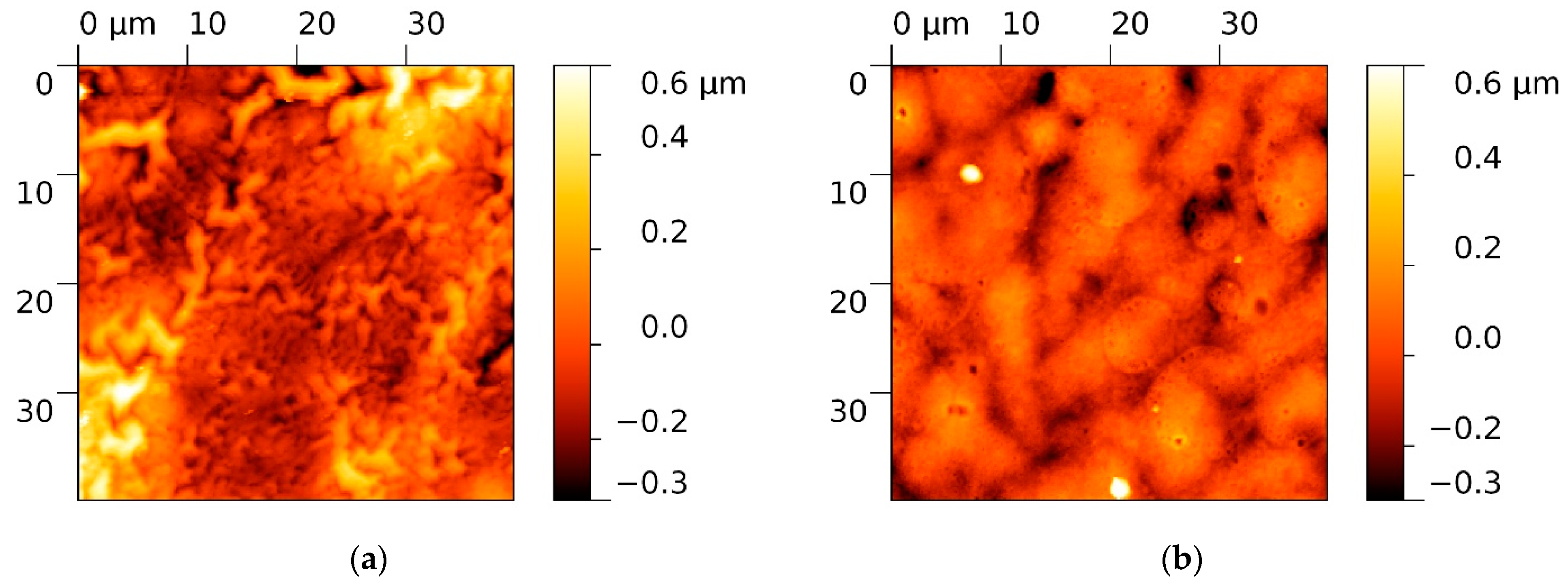
In order to print the SnO2 and Pd-SnO2 pixels, reproducible donor films from SnCl2(acac)2 and Pd(acac)2 precursors are fabricated. Two types of donors based on SnCl2(acac)2 are fabricated, which have distinctive morphologies: (i) “wrinkle”-like structures with predominant valleys (Rsk = −1.105) that induce a high roughness (Rq = 156.17 nm) of the SnCl2(acac)2 thin layer (Figure 2a) and (ii) a relatively flat surface with an almost symmetrical height distribution (as indicated by the Rsk value close to zero), with lower roughness (Rq = 97.25 nm) and with valleys, as revealed by the negative value of Rsk (−0.379) that characterize the Pd-SnCl2(acac)2 donor surface. On a large area (40 µm × 40 µm), the surface of this donor has pores with different sizes (0.3–2.5 µm) (Figure 2b).
The parameters describing the surface morphology (Rq, Min, Max, Rsk), as extracted from AFM scans, are collected in Table 1. The average squared roughness value (Rq) represents the standard deviation of the height value in the selected region, Min is the minimum height value of the scanned region and Max is the maximum height value of the region. Another important parameter that can be extracted from AFM investigation is the skewness (Rsk). Skewness is used to measure the profile symmetry about mean line. When the height distribution is symmetrical, Rsk is zero. If the height distribution is asymmetrical, and the surface has more peaks than valleys, the skewness moment is positive, and if the surface is more planar and valleys are predominant, the Rsk is negative.
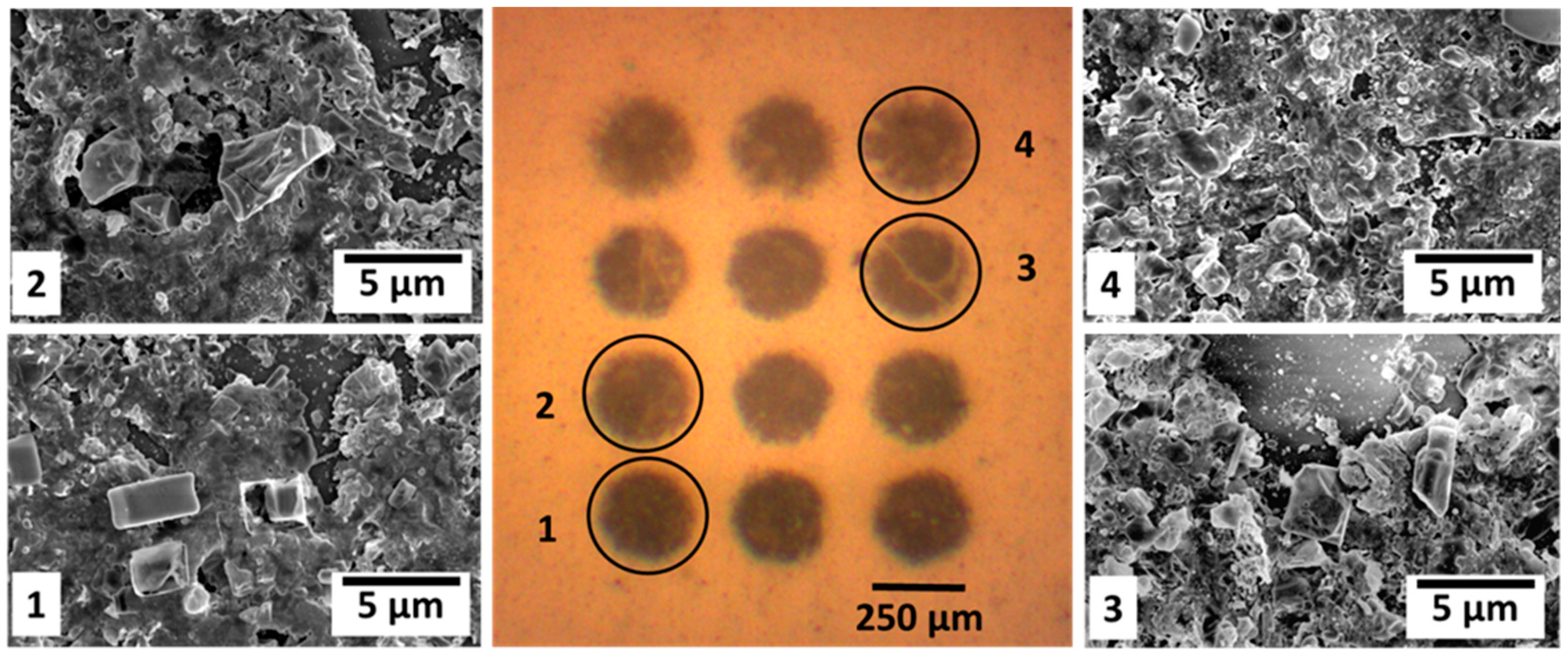
Once reproducible donors are obtained, laser-induced forward transfer is applied to transfer SnO2 and Pd-SnO2 pixels onto glass substrates. The fluence is varied over a broad range, i.e., from conditions insufficient to break the donor layer to high irradiation fluences (250 mJ/cm2), in order to optimize the shape of the transferred pixels. The threshold fluence for the complete removal and transfer of either SnO2 or Pd-SnO2 thin films from the irradiated area (250 µm in diameter spot) is 100 mJ/cm2. All transferred pixels have a circular shape, are regularly arranged, and in some cases, the edges are less uniform, e.g., the pixels at 200 and 250 mJ/cm2 have a negligible amount of material scattered outside the pixel area. We found that the transfer of Pd-SnO2 pixels occurs for the same conditions as for SnO2. An example of optical micrographs of the Pd-SnO2 pixels obtained immediately after transfer at different laser fluences are displayed in Figure 3.
An in-depth investigation of the topography is carried out by SEM, which reveals that the distribution of material inside the pixel area is dependent on the laser fluence. The shape and size of the features observed inside the pixel range from nano-polyhedrons, to near corner-grown cubic Pd-SnO2, or near cubic Pd-SnO2. The high magnification micrographs recorded on the selected pixels, marked 1–4 in Figure 3, reveal the surface morphology and topography of the transferred layer, which was originally the bottom part of the Pd-SnCl2(acac)2 donor target. Although the transferred material covers the substrate, there are distinguishable visible voids on the pixels’ surface. Noticeably, the number, shape and size of the distinguished voids varies from the pixel marked 1 to pixel 4. While the surface of pixel 1 appears to be coarse and includes a large amount of micro-porosity, the surface of pixel 2 is characterized by a smooth topography and visible macro-porosities. Furthermore, large size cavities are visible on the surfaces of pixel 3 and 4. Some crystalline aggregates are visible on the surface of the transferred layer, as shown in Figure 3. Interestingly, both the density and size of the observed crystals seems to gradually increase from pixel 1 to pixel 4. Another finding in Figure 3 (pixel 3 & 4) is the coincidence of the cavity’s shape and size with those of the observed crystals. According to this observation, it seems that the observed large cavities on the pixel 3 & 4 surfaces (dashed arrow) are formed by crystals pulled out (solid arrow) during the LIFT process.
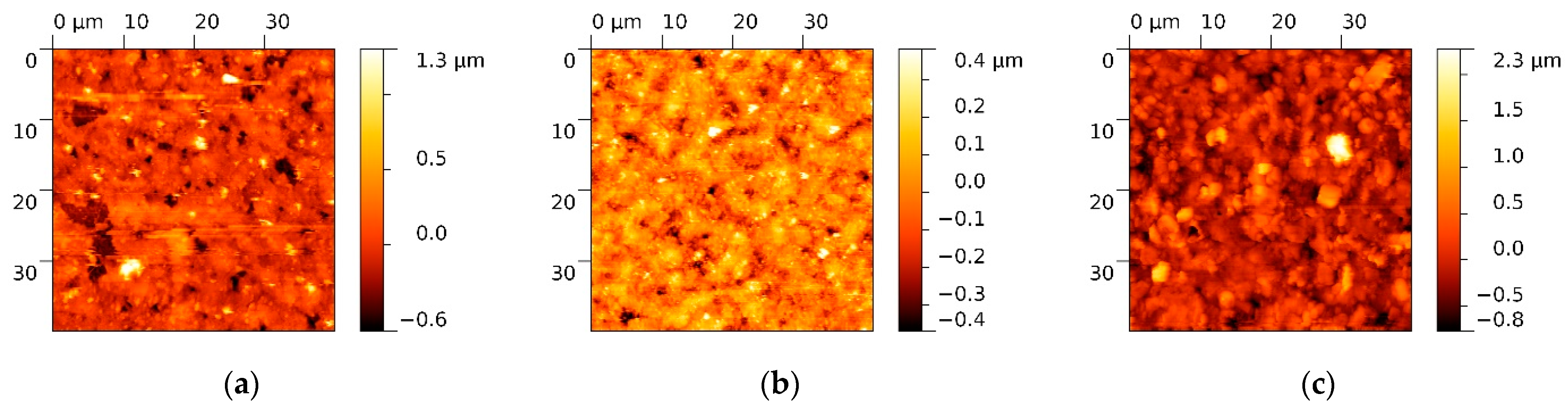
Furthermore, SnO2 and Pd-SnO2 pixels have been transferred at 100 mJ/cm2 laser fluence onto the commercially carbon electrodes in order to further test their functionality by typical cyclic voltammetry. An example of a transferred SnO2 and Pd-SnO2 pixel onto the surface of the working electrode is shown in Figure 4. Both the SnO2 and Pd-SnO2 transferred pixel morphology presents irregular grains with micrometric sizes (1–1.5 µm) and large agglomerations (>5 µm). The scanned surface is relatively planar with an almost symmetrical height distribution (Rsk value close to zero), with high roughness (Rq = 412 nm) and valleys (revealed by the negative value of Rsk).
The differences between the surface morphology of the donor layers (i.e., SnCl2(acac)2 and Pd-SnCl2(acac)2) and the surface morphology of the transferred material appear due to the transformation of the metal precursor to SnO2 and Pd-SnO2 during laser transfer as a result of the photochemical and thermal processes.
3.2. Chemical Investigation
The scope of this study is to demonstrate the fabrication of a proof-of-concept system where commercially available electrodes are decorated with thin film pixels by rLIFT technique. In this section, we aim at describing the chemical states of Pd and Sn from the transferred SnO2 and Pd-SnO2 pixels in order to provide more chemical information for improving the sensitivity of the sensor.
First, in order to assess any modification in the elemental composition by the transfer process, a set of EDX analyses are carried out on the selected pixels from Figure 3. The EDX spectra recorded on pixel 1, which is similar, in terms of detected elements, to the spectra belonging to pixels 2–4, is shown in Figure 5.
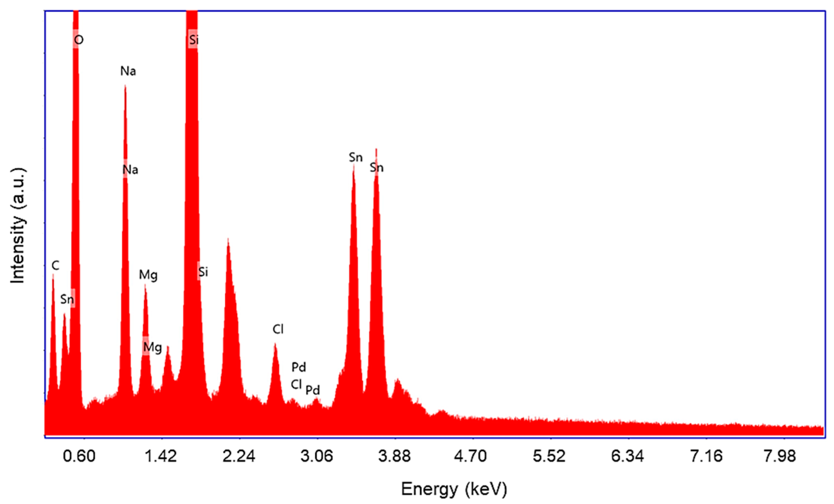
The EDX analysis reveals that the transferred material consists of O, Sn and Pd elements. However, there were also detected Na, K, Mg and Cl elements as originated from the target donor synthesis process. The detected Si is, of course, attributed to glass used as pixel substrate. The C peak in EDX spectra is due to some C cross-contamination during the sample handling process. The EDX spectra includes two non-labelled visible peaks. The first of them, located at 2.3 keV, is attributed to Au used as charge mitigation element for SEM analysis. The other one, located at 1.48 keV, is attributed to the Al sample-holder.
The entire acquired EDX spectra are software processed (TEAM software, AMETEK-EDAX Inc., Mahwah, NJ, USA) utilizing the eZAF algorithm for standardless quantitative analysis of Pd, Sn and O elements in the transferred pixels 1–4. The results obtained are shown in Table 2. In the standardless quantitative process of element determination, all identified compositions are taken into account, but only the elements of interest are quantified (O, Pd and Sn) by resuming them to 100.
The as computed results highlights that the Pd content is gradually increasing from pixel 1 to pixel 4.
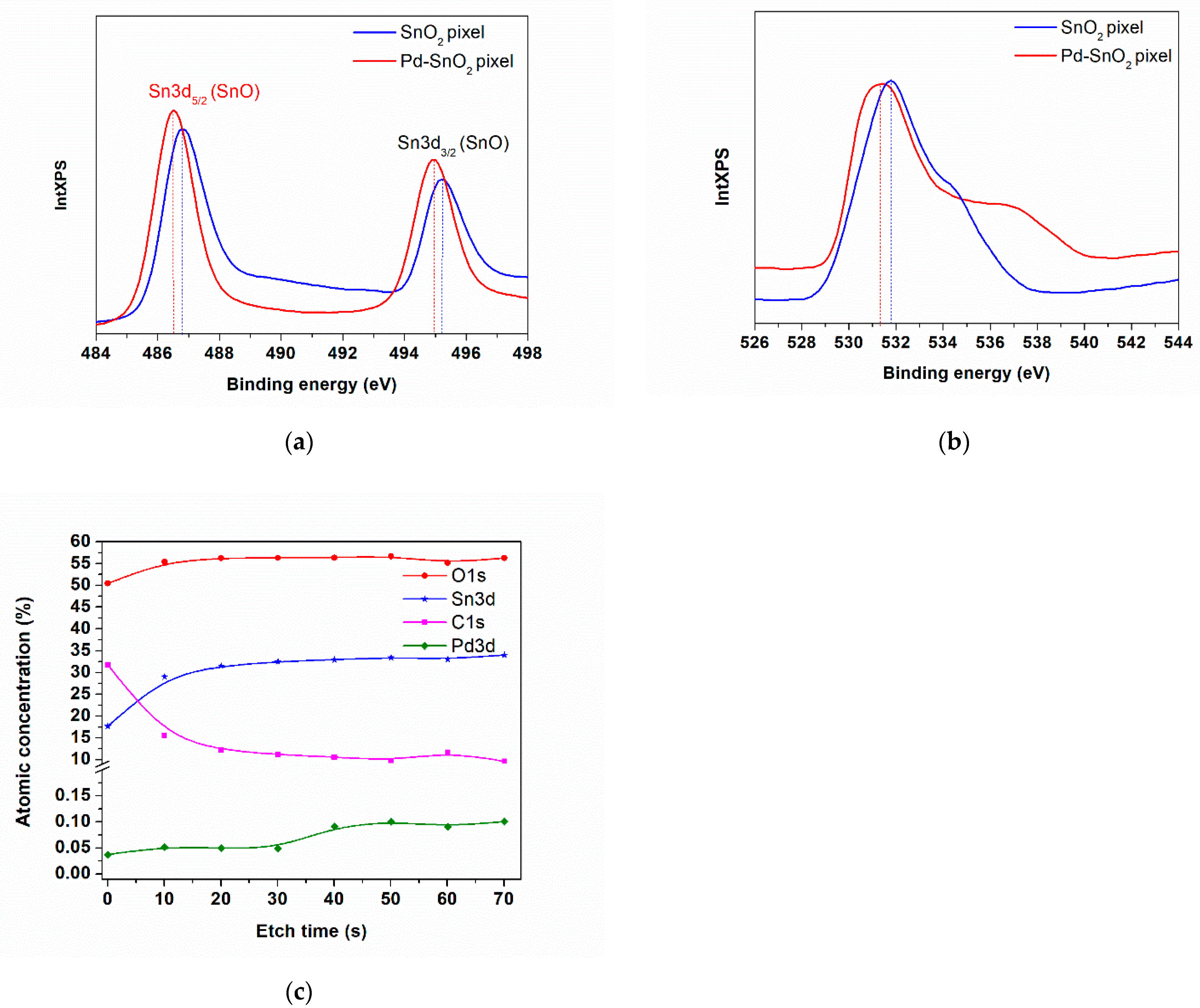
As shown in Table 2, while the quantification error of O, an Sn element, is in the range of the standardless method, i.e., 3–10% [40], the quantification error of the Pd element is noticeably higher for pixel 1 and pixel 2. The origin of this increased error is, of course, related to the pixel 1 & 2 surfaces’ roughness, as revealed through AFM and SEM analysis. Further on, XPS is used to analyze the chemical composition and the nature of the chemical bonds of both the SnO2 and Pd-SnO2 pixel surfaces. The XPS spectra of the SnO2 and Pd-SnO2 pixels together with the atomic concentrations (shown in Table 3) of the SnO2 pixels transferred by LIFT at 100 mJ/cm2 laser fluence is shown in Figure 6a–c and Table 3, and is consistent with those reported elsewhere [41,42,43]. Spin–orbit doublet peaks at ≃486 eV (Sn2+ 3d5/2) and ≃495 eV (Sn2+ 3d3/2) can be observed in the Sn 3d spectra. As can be observed from Figure 6, the binding energies of both the Sn 3d5/2 and Sn 3d3/2 peaks for the SnO2 and Pd-SnO2 pixels have different values (i.e., 486.1 eV and 495.22 eV for SnO2 and 486.49 eV and 494.97 eV for Pd-SnO2). The trend of decreasing the binding energies of Sn 3d5/2 (by −0.3 eV in our case) by doping Pd in SnO2 has been reported earlier [43]. Although the mechanism has not been completely elucidated, the decrease in the Fermi level of the SnO2 is attributed to the role of electronic sensitizer of the Pd. The same observation can be made for the O1s peak of SnO2 as compared to the O1s peak of the Pd-SnO2 pixel (i.e., 531.74 eV for SnO2 and 531.3 eV for Pd-SnO2). The O1s peak of both SnO2 and Pd-SnO2 pixels is asymmetric and exhibits an evident shoulder in the higher binding energy part, as shown in Figure 6b, which could be attributed to the oxygen atoms chemisorbed at the surface [42]. Furthermore, due to the fact that no Pd peak could be found at the surface of the Pd-SnO2 pixels, we investigated the evolution of the O, C, Sn and Pd as a function of etching time, and our results are consistent with those from EDX, where an amount lower than 0.5% of Pd is present in the transferred pixels.
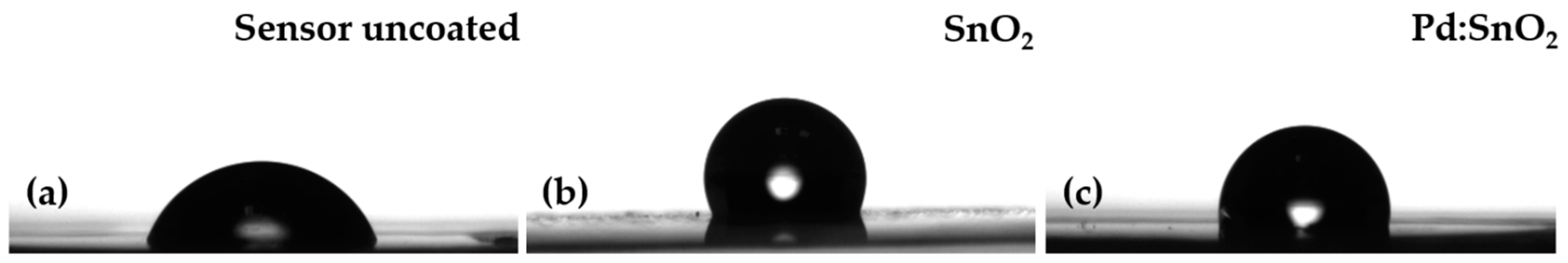
Contact angle (CA) measurements are carried out to understand the surface wetting properties of the sensing electrode. The images of the water droplets on the uncoated, SnO2 and Pd-SnO2 coated sensors are shown in Figure 7.
The contact angle of the uncoated sensor is 69.75° ± 0.69°, whilst the contact angle for the SnO2 coated sensor is 101.77° ± 0.24° and 95.4° ± 1.21° for Pd-SnO2, respectively. The increase of the CA shows that the surface is more hydrophobic which is advantageous for self-cleaning of the sensor. Significantly, it demonstrates that the rLIFT results in a different surface wetting property, which is advantageous for any adsorption-based sensor development.
3.3. Assessment of the LIFT Modified Electrodes Functionality
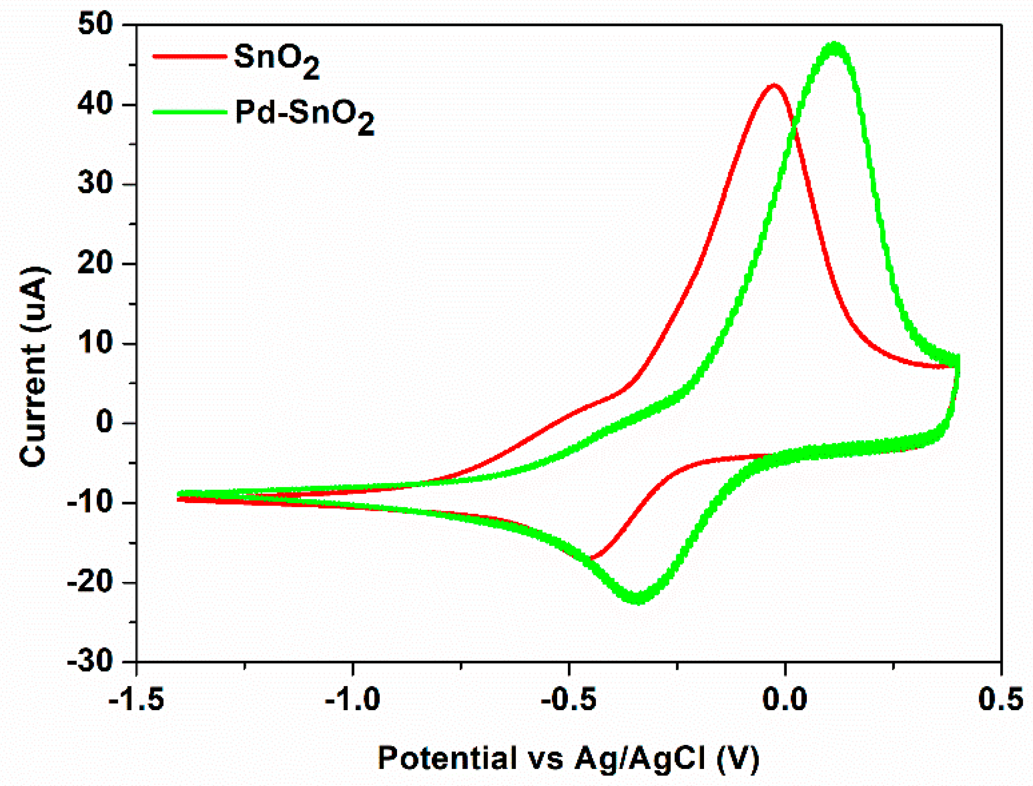
A typical cyclic volammogram of 100 ppm Cu2+ in 0.1 M acetate buffer solution (pH = 5.0 upH) obtained by using modified flexible screen-printed electrodes (SPE) based on PEDOT as working electrode is presented in Figure 8, the resulting data being presented in Table 4.
A single cathodic peak, Ipc is obtained during the forward scan at in the range of −476 mV → −330 mV, the Cu2+ being reduced to Cu0 by a two-electron transfer reaction (Cu2+ + 2e− → Cu0). This is in good agreement with the study reported by Shaikh et. al., where they have demonstrated that bivalent copper is directly reduced to metallic copper in electrolyte solutions having pH > 4.08 [44]. In addition, the oxidation of copper (Cu0 → Cu2+ + 2e−) is observed during the reverse, with an anodic peak at around +45 mV.
As can be observed in Table 4 the addition of SnO2 to the commercial SPE leads to a small decrease of both anodic and cathodic peaks current. The peak potential separation (∆Ep) decreases to 429 mV, the sample showing a negative value of −31 mV for the anodic peak potential. The ratio between the current peaks is also lower (2.90) compared to the obtained value for the bare SPE. The addition of Pd nanoparticles to the SnO2-SPE sensor leads to an increase of the currents, especially for the cathodic peak. This reveals that the addition of Pd to SnO2 may provide the required conduction pathways at the surface of the electrode and ensures better electrochemical behavior. The peak potential separation is the same as that obtained for the commercial SPE and the current ratio is increased.
4. Conclusions
In this work, the combination of low-cost materials together with a facile and cost-efficient method to modify flexible electrodes for the detection of Cu ions has been evaluated. In particular, SnO2 and Pd-SnO2 thin film pixels were evaluated for their potential to amplify the signal of an electrochemical working electrode. Both the SnO2 and Pd-SnO2 thin film pixels were obtained by laser-induced forward transfer (LIFT) from metal acetylacetonates precursors which are decomposed under UV light. Extensive evaluation of the morphological and chemical properties of the transferred materials reveals that LIFT was successfully applied to obtain chemically stable SnO2 and Pd-SnO2 pixels which exhibit a high roughness. In addition, the contact angle measurements carried out onto the transferred SnO2 and Pd-SnO2 pixels highlight the possibility to tune the wettability of the screen-printed electrodes (SPE) by LIFT.
Finally, compared to the bare screen-printed electrodes, the addition of Pd nanoparticles to the SnO2-SPE sensor, leads to an increase of the currents, especially for the cathodic peak. Thus, the LIFT fabricated Pd-SnO2 electrodes could be used as a classic sensor for Cu ions detection. This result also suggests that this simple method could be used for decoration and modification of electrodes for the detection of other toxic ions.
Author Contributions
Conceptualization, A.P.-P.; methodology, F.A., I.B., M.F. and A.P.-P.; validation, F.A., I.B., M.F. and A.P.-P.; formal analysis, F.A., I.B., M.F. and A.P.-P.; data curation, F.A., I.B., M.F. and A.P.-P.; writing—original draft preparation, F.A., I.B., M.F. and A.P.-P.; writing—review and editing, F.A., I.B., M.F. and A.P.-P.; project administration, A.P.-P.; funding acquisition, A.P.-P. All authors have read and agreed to the published version of the manuscript.
Funding
This work was supported by a grant of the Ministry of Education and Research, CNCS-UEFISCDI, project number PN-III-P1-1.1-TE-2016-1417 (iFLEX) within PNCDI III, the Ministry of Research, Innovation and Digitalization through Program I—Development of the National R & D System, Subprogram 1.2–Institutional Performance–Projects for Excellence Financing in RDI, contract no. 13PFE/2021, and the Romanian National Nucleus Program.
Institutional Review Board Statement
Not applicable.
Informed Consent Statement
Not applicable.
Data Availability Statement
The data used to support the findings of this study are available from the corresponding author upon request.
Acknowledgments
The authors are grateful to Veronica Satulu for helping to acquire the XPS spectra and Simona Brajnicov for helping to acquire the contact angle measurements.
Conflicts of Interest
The authors declare no conflict of interest.
References
- Sodhi, R.K.; Paul, S. An Overview of Metal Acetylacetonates: Developing Areas/Routes to New Materials and Applications in Organic Syntheses. Catal. Surv. Asia 2018, 22, 31–62. [Google Scholar] [CrossRef]
- Caille, J.-R.; Debuigne, A.; Jérôme, R. Quinone Transfer Radical Polymerization (QTRP) of Styrene: Catalysis by Different Metal Complexes. J. Polym. Sci. Part A Polym. Chem. 2005, 43, 2723–2733. [Google Scholar] [CrossRef]
- Chua, M.L.; Xiao, Y.; Chung, T.S. Using Iron (III) Acetylacetonate as Both a Cross-Linker and Micropore Former to Develop Polyimide Membranes with Enhanced Gas Separation Performance. Sep. Purif. Technol. 2014, 133, 120–128. [Google Scholar] [CrossRef]
- Kucharyson, J.F.; Cheng, L.; Tung, S.O.; Curtiss, L.A.; Thompson, L.T. Predicting the Potentials, Solubilities and Stabilities of Metal-Acetylacetonates for Non-Aqueous Redox Flow Batteries Using Density Functional Theory Calculations. J. Mater. Chem. A 2017, 5, 13700–13709. [Google Scholar] [CrossRef]
- Kaneko, T.; Watanuki, Y.; Toyama, T.; Kojima, Y.; Nishimiya, N. Characterization and Hydrogen Sorption Behaviors of FeNiCr-Carbon Composites Derived from Fe, Ni and Cr-Containing Polyacrylonitrile Fibers Prepared by Electrospinning Method. Int. J. Hydrogen Energy 2017, 42, 10014–10022. [Google Scholar] [CrossRef]
- Inagaki, N.; Tasaka, S.; Nozue, Y. Plasma Polymerization of Metal Acetylacetonates and Application for Gas Sensor Devices. J. Appl. Polym. Sci. 1992, 45, 1041–1048. [Google Scholar] [CrossRef]
- Goncharov, T.; Nasriddinov, A.; Zubenko, A.; Tokarev, S.; Shatalova, T.; Khmelevsky, N.; Fedorova, O.; Rumyantseva, M. Nanocrystalline SnO2 Functionalized with Ag(I) Organometallic Complexes as Materials for Low Temperature H2S Detection. Materials 2021, 14, 7778. [Google Scholar] [CrossRef]
- Kamedulski, P.; Skorupska, M.; Binkowski, P.; Arendarska, W.; Ilnicka, A.; Lukaszewicz, J.P. High surface area micro-mesoporous graphene for electrochemical applications. Sci. Rep. 2021, 11, 22054. [Google Scholar] [CrossRef]
- Vasiliev, V.P.; Manzhos, R.A.; Kochergin, V.K.; Krivenko, A.G.; Kabachkov, E.N.; Kulikov, A.V.; Shulga, Y.M.; Gutsev, G.L. A Facile Synthesis of Noble-Metal-Free Catalyst Based on Nitrogen Doped Graphene Oxide for Oxygen Reduction Reaction. Materials 2022, 15, 821. [Google Scholar] [CrossRef]
- Alwin, E.; Kočí, K.; Wojcieszak, R.; Zieliński, M.; Edelmannová, M.; Pietrowski, M. Influence of High Temperature Synthesis on the Structure of Graphitic Carbon Nitride and Its Hydrogen Generation Ability. Materials 2020, 13, 2756. [Google Scholar] [CrossRef]
- Holder, E.; Langeveld, B.M.W.; Schubert, U.S. New Trends in the Use of Transition Metal-Ligand Complexes for Applications in Electroluminescent Devices. Adv. Mater. 2005, 17, 1109–1121. [Google Scholar] [CrossRef]
- El-Mahalawy, A.M. Structural and Optical Characteristics of Nickel Bis(Acetylacetonate) Thin Films as a Buffer Layer for Optoelectronic Applications. Mater. Sci. Semicond. Process. 2019, 100, 145–158. [Google Scholar] [CrossRef]
- Taheri, M.; Naderi, R.; Saremi, M.; Mahdavian, M. Development of an Ecofriendly Silane Sol-Gel Coating with Zinc Acetylacetonate Corrosion Inhibitor for Active Protection of Mild Steel in Sodium Chloride Solution. J. Sol.-Gel. Sci. Technol. 2017, 81, 154–166. [Google Scholar] [CrossRef]
- Ortiz, A.; Alonso, J.C.; Haro-Poniatowski, E. Spray Deposition and Characterization of Zirconium-Oxide Thin Films. J. Electron. Mater. 2005, 34, 150–155. [Google Scholar] [CrossRef]
- Chang, Q.; Zhang, N.; Liu, W.; Ye, Q.; Yu, Y.; Chen, X.; Li, C. Thermal Properties and Gas Decomposition Products of Hafnium(IV) Acetylacetonate. Asian J. Chem. 2010, 22, 1935–1938. [Google Scholar]
- Singhal, A.; Sanyal, B.; Tyagi, A.K. Tin Oxide Nanocrystals: Controllable Synthesis, Characterization, Optical Properties and Mechanistic Insights into the Formation Process. RSC Adv. 2011, 1, 903–910. [Google Scholar] [CrossRef]
- Adedeji, A.V.; Egharevba, G.O.; Jeynes, C.; Ajayi, E.O.B. Preparation and Characterization of Pyrolytically Deposited (Co-V-O and Cr-V-O) Thin Films. Thin Solid Films 2002, 402, 49–54. [Google Scholar] [CrossRef]
- Tsuchiya, T.; Watanabe, A.; Imai, Y.; Niino, H.; Yabe, A.; Yamaguchi, I.; Manabe, T.; Kumagai, T.; Mizuta, S. Preparation of Metal Oxide Thin Films Using Coating Photolysis Process with ArF Excimer Laser. In Proceedings of the 1st International Symposium on Laser Precision Microfabrication; Miyamoto, I., Sugioka, K., Sigmon, T.W., Eds.; Spie-Int Soc Optical Engineering: Bellingham, WA, USA, 2000; Volume 4088, pp. 311–314. [Google Scholar]
- Gil-Rostra, J.; Yubero, F.; Ferrer, F.J.; González-Elipe, A.R. Combined Reactive Magnetron Sputtering and Plasma Decomposition of Non-Volatile Precursors to Grow Luminescent Thin Films. Surf. Coat. Technol. 2013, 222, 144–150. [Google Scholar] [CrossRef]
- Arnold, C.B.; Serra, P.; Pique, A. Laser Direct-Write Techniques for Printing of Complex Materials. MRS Bull. 2007, 32, 23–31. [Google Scholar] [CrossRef] [Green Version]
- Springer, M.; Dusing, J.; Koch, J.; Jaschke, P.; Kaierle, S.; Overmayer, L. Laser-Induced Forward Transfer as a Potential Alternative to Pick-and-Place technology when Assembling Semiconductor Components. J. Laser Appl. 2021, 33, 042030. [Google Scholar] [CrossRef]
- Sammartino, C.; Sedghani Cohen, S.; Kotler, Z.; Eliaz, N. Direct Writing of High-Resolution, High-Quality Pure Metal Patterns on Smooth Transparent Substrates by Laser-induced Forward Transfer Followed by a Novel Laser Treatment. Adv. Eng. Mater. 2021, 23, 2100245. [Google Scholar] [CrossRef]
- Wang, X.; Zheng, J.; Mei, X.; Xu, B.; Miao, J. Laser Fabrication of fully Printed Graphene Oxide Microsensor. Opt. Lasers Eng. 2021, 140, 106520. [Google Scholar] [CrossRef]
- Delaporte, P.; Alloncle, A.-P. Laser-induced forward transfer: A high resolution additive manufacturing technology. Opt. Laser Technol. 2016, 78, 33–41. [Google Scholar] [CrossRef]
- Serra, P.; Duocastella, M.; Fernández-Pradas, J.M.; Morenza, J.L. Liquids microprinting through laser-induced forward transfer. Appl. Surf. Sci. 2009, 255, 5342–5345. [Google Scholar] [CrossRef]
- Palla-Papavlu, A.; Patrascioiu, A.; Di Pietrantonio, F.; Fernández-Pradas, J.-M.; Cannatà, D.; Benetti, M.; D’Auria, S.; Verona, E.; Serra, P. Preparation of surface acoustic wave odor sensors by laser-induced forward transfer. Sens. Actuators B Chem. 2014, 192, 369–377. [Google Scholar] [CrossRef]
- Gorodesky, N.; Sedghani-Cohen, S.; Fogel, O.; Silber, A.; Tkachev, M.; Kotler, Z.; Zalevsky, Z. Improving Compactness of 3D Metallic Microstructures Printed by Laser-Induced Forward Transfer. Crystals 2021, 11, 291. [Google Scholar] [CrossRef]
- Visser, C.W.; Pohl, R.; Sun, C.; Roemer, G.-W.; in ’t Veld, B.H.; Lohse, D. Toward 3D Printing of Pure Metals by Laser-Induced Forward Transfer. Adv. Mater. 2015, 27, 4087–4092. [Google Scholar] [CrossRef] [Green Version]
- Mills, B.; Heath, D.J.; Feinaeugle, M.; Eason, R.W. LIFT of Solid Films (Ceramics and Polymers). In Laser Printing of Functional Materials; John Wiley & Sons, Ltd.: Hoboken, NJ, USA, 2018; pp. 175–198. ISBN 978-3-527-80510-5. [Google Scholar]
- Makrygianni, M.; Zacharatos, F.; Andritsos, K.; Theodorakos, I.; Reppas, D.; Oikonomidis, N.; Spandonidis, C.; Zergioti, I. Eco-Friendly Lead-Free Solder Paste Printing via Laser-Induced Forward Transfer for the Assembly of Ultra-Fine Pitch Electronic Components. Materials 2021, 14, 3353. [Google Scholar] [CrossRef]
- Papazoglou, S.; Zergioti, I. Laser Induced Forward Transfer (LIFT) of Nano-Micro Patterns for Sensor Applications. Microelectron. Eng. 2017, 182, 25–34. [Google Scholar] [CrossRef]
- Shaw Stewart, J.; Lippert, T.; Nagel, M.; Nüesch, F.; Wokaun, A. Red-Green-Blue Polymer Light-Emitting Diode Pixels Printed by Optimized Laser-Induced Forward Transfer. Appl. Phys. Lett. 2012, 100, 203303. [Google Scholar] [CrossRef] [Green Version]
- Charipar, K.M.; Charipar, N.A.; Prestigiacomo, J.C.; Bingham, N.S.; Pique, A. Laser Printing of Flip-Chip Interconnects for High Frequency Applications. J. Manuf. Process. 2018, 32, 110–115. [Google Scholar] [CrossRef]
- Nastulyavichus, A.; Tolordava, E.; Rudenko, A.; Zazymkina, D.; Shakhov, P.; Busleev, N.; Romanova, Y.; Ionin, A.; Kudryashov, S. In Vitro Destruction of Pathogenic Bacterial Biofilms by Bactericidal Metallic Nanoparticles via Laser-Induced Forward Transfer. Nanomaterials 2020, 10, 2259. [Google Scholar] [CrossRef] [PubMed]
- Soulis, D.; Trigazi, M.; Tsekensis, G.; Chandrinou, C.; Klinakis, A.; Zergioti, I. Facile and Low-Cost SPE Modification Towards Ultra-Sensitive Organophosphorous and Carbamate Pesticide Detection in Olive Oil. Molecules 2020, 25, 4988. [Google Scholar] [CrossRef] [PubMed]
- Mattle, T.; Shaw-Stewart, J.; Hintennach, A.; Schneider, C.W.; Lippert, T.; Wokaun, A. Shadowgraphic Investigations into the Laser-Induced Forward Transfer of Different SnO2 Precursor Films. Appl. Surf. Sci. 2013, 278, 77–81. [Google Scholar] [CrossRef]
- Mattle, T.; Hintennach, A.; Lippert, T.; Wokaun, A. Laser induced forward transfer of SnO2 for sensing applications using different precursors systems. Appl. Phys. A 2013, 110, 309–316. [Google Scholar] [CrossRef]
- Palla Papavlu, A.; Mattle, T.; Temmel, S.; Lehmann, U.; Hintennach, A.; Grisel, A.; Wokaun, A.; Lippert, T. Highly Sensitive SnO2 Sensor via Reactive Laser-Induced Transfer. Sci. Rep. 2016, 6, 25144. [Google Scholar] [CrossRef] [Green Version]
- Gschwend, P.M.; Schenk, F.M.; Gogos, A.; Pratsinis, S.E. Acetone Sensing and Catalytic Conversion by Pd-Loaded SnO2. Materials 2021, 14, 5921. [Google Scholar] [CrossRef]
- Labar, J.L. Standardless Quantitative Analysis by X-Ray Spectrometry. Scanning Microsc. 1993, 1993, 10. [Google Scholar]
- Ansell, R.O.; Dickinson, T.; Povey, A.F.; Sherwood, P.M.A. Quantitative use of the angular variation technique in studies of tin by X-ray photoelectron spectroscopy. J. Electron. Spectros. Relat. Phenom. 1977, 11, 301–313. [Google Scholar] [CrossRef]
- Szuber, J.; Czempik, G.; Larciprete, R.; Koziej, D.; Adamowicz, B. XPS study of the L-CVD deposited SnO2 thin films exposed to oxygen and hydrogen. Thin Solid Films 2001, 391, 198–203. [Google Scholar] [CrossRef]
- Cao, X.; Cao, L.; Yao, W.; Ye, X. Structural Characterization of Pd-doped SnO2 Thin Films Using XPS. Surf. Interface Anal. 1996, 24, 662–666. [Google Scholar] [CrossRef]
- Shaikh, A.A.; Firdaws, J.; Badrunnessa; Serajee, S.; Rahman, M.S.; Bakshi, P.K. Electrochemical Studies of the PH Dependence of Cu(II) Reduction in Aqueous Britton-Robinson Buffer Solution. Int. J. Electrochem. Sci. 2011, 6, 2333–2343. [Google Scholar]
- Haque, F.; Rahman, M.S.; Ahmed, E.; Bakshi, P.; Shaikh, A. A Cyclic Voltammetric Study of the Redox Reaction of Cu(II) in Presence of Ascorbic Acid in Different PH Media. Dhaka Univ. J. Sci. 2013, 61, 161–166. [Google Scholar] [CrossRef] [Green Version]
- Mei, C.J.; Yusof, N.A.; Ahmad, S.A.A. Electrochemical Determination of Lead & Copper Ions Using Thiolated Calix[4]Arene-Modified Screen-Printed Carbon Electrode. Chemosensors 2021, 9, 157. [Google Scholar] [CrossRef]
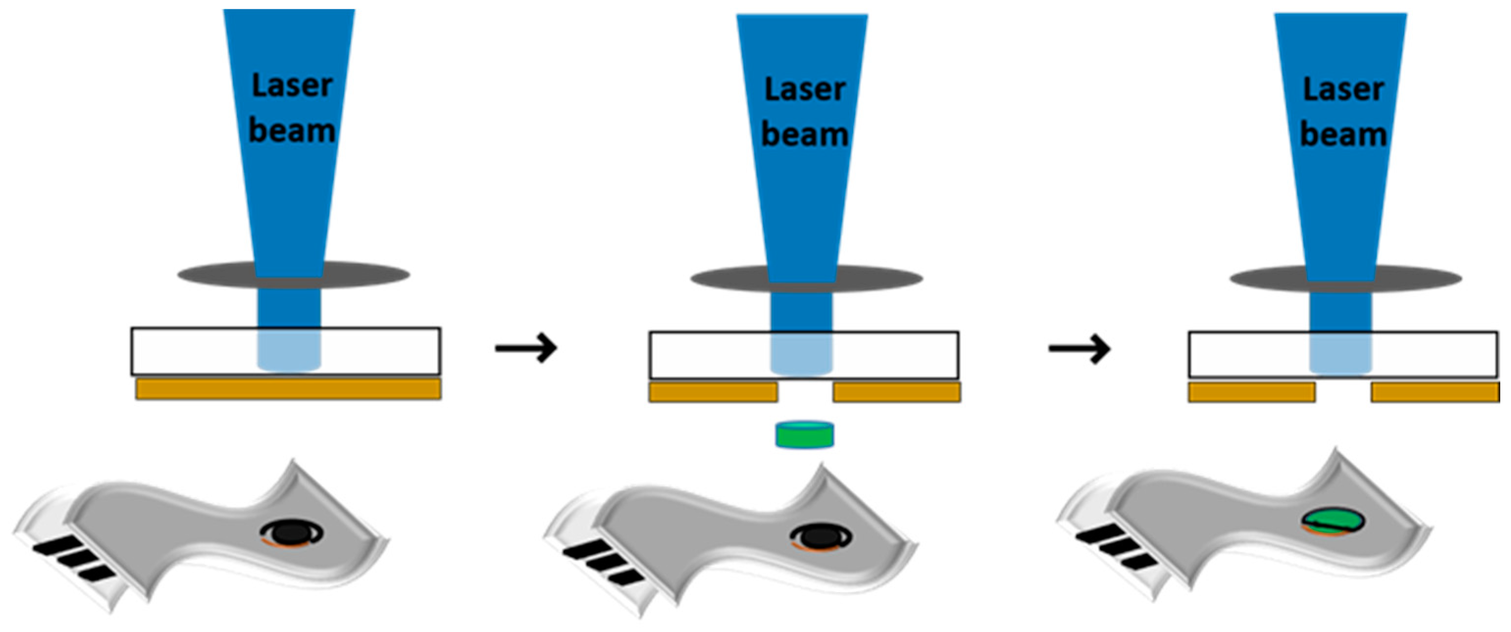
Figure 1.
Scheme of the LIFT process for printing SnO2 and Pd-SnO2 pixels from SnCl2(acac)2 and Pd-SnO2 donors onto flexible electrochemical electrodes.
Figure 1.
Scheme of the LIFT process for printing SnO2 and Pd-SnO2 pixels from SnCl2(acac)2 and Pd-SnO2 donors onto flexible electrochemical electrodes.

Figure 2.
AFM images of the (a) SnCl2(acac)2 donor surface, (b) Pd-SnCl2(acac)2 donor surface.

Figure 3.
(Center image) Optical microscopy image of a Pd-SnO2 pixel array obtained by varying the laser fluence between 100 mJ/cm2 (lowest row) and 250 mJ/cm2 (top row). Images 1–4 represent scanning electron microscopy images taken in the middle of the Pd-SnO2 pixel transferred at: image 1—100 mJ/cm2; image 2—150 mJ/cm2; image 3—200 mJ/cm2; and image 4—250 mJ/cm2.

Figure 4.
AFM images of (a) clean surface of the working electrode, (b) SnO2 pixel transferred at 100 mJ/cm2 laser fluence on the surface of the working electrode, and (c) Pd-SnO2 pixel transferred at 100 mJ/cm2 laser fluence on the surface of the working electrode.
Figure 4.
AFM images of (a) clean surface of the working electrode, (b) SnO2 pixel transferred at 100 mJ/cm2 laser fluence on the surface of the working electrode, and (c) Pd-SnO2 pixel transferred at 100 mJ/cm2 laser fluence on the surface of the working electrode.

Figure 5.
Typical EDX spectra recorded on the transferred Pd-SnO2 pixels.

Figure 6.
(a) Sn 3d, (b) O1s core-level XPS spectra of SnO2 and Pd-SnO2 pixels transferred at 100 mJ/cm2; (c) Evolution of O, C, Sn and Pd as a function of etching time.
Figure 6.
(a) Sn 3d, (b) O1s core-level XPS spectra of SnO2 and Pd-SnO2 pixels transferred at 100 mJ/cm2; (c) Evolution of O, C, Sn and Pd as a function of etching time.

Figure 7.
Contact angle images for (a) the uncoated working electrode, (b) the working electrode coated with a SnO2 pixel and (c) the working electrode coated with a Pd-SnO2 pixel.
Figure 7.
Contact angle images for (a) the uncoated working electrode, (b) the working electrode coated with a SnO2 pixel and (c) the working electrode coated with a Pd-SnO2 pixel.

Figure 8.
Cyclic voltammograms of Cu2+ (100 ppm) in 0.1 M acetate buffer solution (pH = 5.0) recorded on red SPE-based SnO2 and green SPE-based Pd-SnO2.
Figure 8.
Cyclic voltammograms of Cu2+ (100 ppm) in 0.1 M acetate buffer solution (pH = 5.0) recorded on red SPE-based SnO2 and green SPE-based Pd-SnO2.


Table 1.
AFM parameters that describe the surface morphology for (40 µm × 40 µm) scanned areas.
| Donor | Min (nm) | Max (nm) | Rq (nm) | Rsk | Thickness (nm) |
|---|---|---|---|---|---|
| SnCl2(acac)2 | −457.323 | 781.542 | 156.176 | −1.105 | 1085 |
| Pd-SnCl2(acac)2 | −519.386 | 781.174 | 97.251 | −0.379 | 895 |
Table 2.
EDX analysis using the standardless ZAF quantification method of Pd, Sn and O elements in the transferred pixels 1–4.
Table 2.
EDX analysis using the standardless ZAF quantification method of Pd, Sn and O elements in the transferred pixels 1–4.
| Pixel 1 | Pixel 2 | Pixel 3 | Pixel 4 | |||||||||
|---|---|---|---|---|---|---|---|---|---|---|---|---|
| Element | wt % | Atomic % | Error % | wt % | Atomic % | Error % | wt % | Atomic % | Error % | wt % | Atomic % | Error % |
| OK | 51.34 | 88.67 | 4.29 | 46.92 | 88.77 | 4.52 | 40.09 | 83.23 | 4.82 | 41.88 | 84.23 | 4.89 |
| PdL | 0.04 | 0.01 | 17.45 | 0.07 | 0.02 | 15.91 | 0.26 | 0.08 | 10.00 | 0.39 | 0.12 | 11.87 |
| SnL | 48.62 | 11.32 | 3.04 | 53.02 | 13.22 | 2.89 | 59.65 | 16.69 | 2.67 | 57.73 | 15.65 | 2.68 |
Table 3.
Atomic concentrations (%) of SnO2 pixels transferred by LIFT at 100 mJ/cm2.
| Sn 3d5 | O1s | C1s |
|---|---|---|
| 20.65 ± 2.5 | 66.3 ± 3.5 | 13.05 ± 4 |
Table 4.
Data obtained from voltammograms recorded for Cu2+ in acetate buffer on different SnO2 and Pd-SnO2 based sensors.
Table 4.
Data obtained from voltammograms recorded for Cu2+ in acetate buffer on different SnO2 and Pd-SnO2 based sensors.
| Sensor | Cu2+ Concentration | pH | Peak Current (μA) | Peak Potential (mV) | ∆Ep = Epa − Epc | |ipa/ipc| | Ref. | ||
|---|---|---|---|---|---|---|---|---|---|
| (−) ipc | ipa | (−) Epc | Epa | ||||||
| Commercial SPE-PEDOT | 100 ppm | 5 | 11.41 | 42.9 | 430 | 26 | 450 | 3.76 | - |
| GCE | ca. 188 ppm | 1.03 | 50.99 | 140.24 | 82 | 53 | 135 | 2.75 | [44] |
| GCE | ca. 135 ppm | 5.3 | 125 | 148.2 | 301.4 | 291.52 | 592.92 | 1.19 | [45] |
| Modified-SPCE | 1 ppm | 8 | - | <2 | - | - | - | - | [46] |
| SnO2 | 100 ppm | 5 | 10.01 | 38.03 | 460 | −31 | 429 | 2.90 | This work |
| Pd-SnO2 | 100 ppm | 5 | 15.18 | 44.06 | 340 | 110 | 450 | 3.79 | This work |
GCE—glassy carbon electrode; SPCE—screen-printed carbon electrode.
Publisher’s Note: MDPI stays neutral with regard to jurisdictional claims in published maps and institutional affiliations. |
© 2022 by the authors. Licensee MDPI, Basel, Switzerland. This article is an open access article distributed under the terms and conditions of the Creative Commons Attribution (CC BY) license (https://creativecommons.org/licenses/by/4.0/).
Share and Cite
MDPI and ACS Style
Andrei, F.; Boerasu, I.; Filipescu, M.; Palla-Papavlu, A. Facile Modification of Flexible Electrodes via Laser Transfer. Materials 2022, 15, 2488. https://0-doi-org.brum.beds.ac.uk/10.3390/ma15072488
AMA Style
Andrei F, Boerasu I, Filipescu M, Palla-Papavlu A. Facile Modification of Flexible Electrodes via Laser Transfer. Materials. 2022; 15(7):2488. https://0-doi-org.brum.beds.ac.uk/10.3390/ma15072488
Chicago/Turabian StyleAndrei, Florin, Iulian Boerasu, Mihaela Filipescu, and Alexandra Palla-Papavlu. 2022. "Facile Modification of Flexible Electrodes via Laser Transfer" Materials 15, no. 7: 2488. https://0-doi-org.brum.beds.ac.uk/10.3390/ma15072488
Note that from the first issue of 2016, this journal uses article numbers instead of page numbers. See further details here.